Individual Assignment
Design a development board to interact and communicate with an embedded microcontroller
extra credit: try another design workflow
extra credit: make a case for it
extra credit: simulate its operation
Group Assignment
Use the test equipment in your lab to observe the operation of a microcontroller circuit board (as a minimum, you should demonstrate the use of a multimeter and oscilloscope)
Document your work on the group work page and reflect what you learned on your individual page
Learning outcomes
- Select and use software for circuit board design
- Demonstrate workflows used in circuit board design
Design a development board to interact and communicate with an embedded microcontroller
For this assignment I wanted to take the opportunity to try different EDA software, specifically SVGPCB , KiCAD and EAGLE. During Global Open Time Rico went over SVGPCB and after following along it seemed pretty straight forward. I also want to try KiCAD since it is open source and at first glance it seems not too difficult to work with. I also intend to spend some time in EAGLE since it is integrated into Fusion and I like to be able to work in a single software for an entire project.
SVGPCB
To keep things simple I decided to recreate Neil´s example of t-412-blink-3 pin board. I started by importing the components I needed, ATtiny412 (ICs/ATtiny412.json), capacitor (discretes/C_1206.json), resistor (discretes/R_1206.json), LED (diodes_transistors_regulators_sensors/LED_1206.json) . I was unable to find the 3 pin UPDI header component so I found Neils example on the SVGPCB example page and copied the js code for the component.
I did not want to spend too much time coming up with my own design, I just wanted to get used to working in SVGPCB so I copied the layout for the board. I placed the ATtiny in the center and used the translate positions for each component based on the ATtiny, so if I move the Tiny around the other components follow. For the wire connections I used code to place the wires exactly on the desired pads. This way if I move things around on the board and the wire connections stay connected.
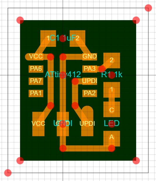
I wanted to play around some more in SVGPCB so I decided to add a button. I add the button component (switches/button_6mm.json) and dragged into the board layout. I fixed the translation position of the button to the Tiny and routed the wires as before.
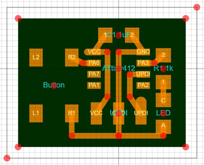
I enjoyed working in SVGPCB and I will most definitely be using it again in the future, especially for simple projects.
KiCAD
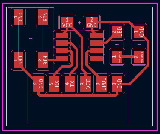
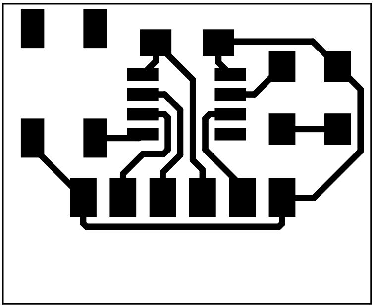
For my first assignment I followed a KiCAD tutorial from Fab Lab Aalto. The tutorial went over all basic commands and how to add the Fab components library and designing the simple hello-t412-echo board from Neil´s example. I followed along and made some changes. I for example did not like how the tutorial used a fill layer to get all the GND connections. Instead I made changes to the sketch, made a different layout and routed each connection.
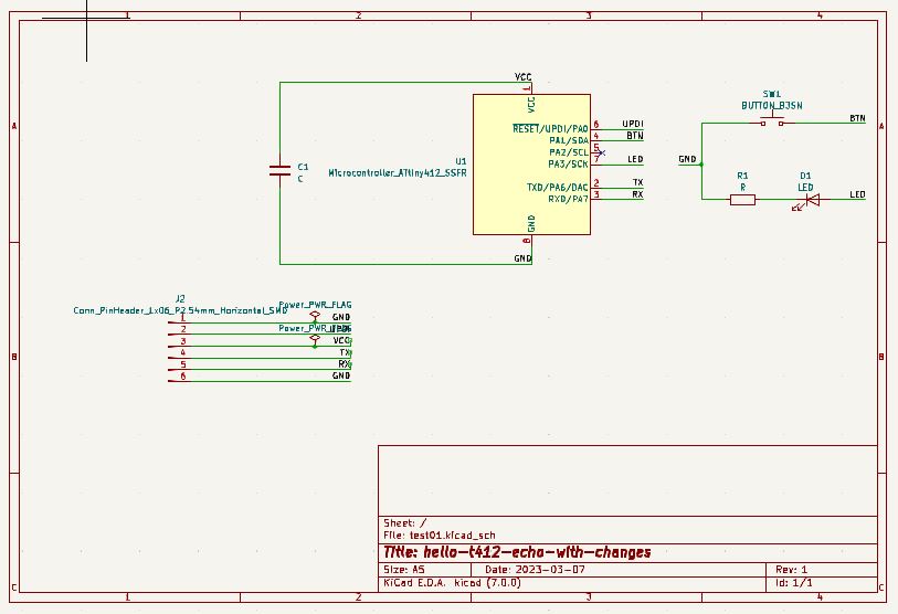
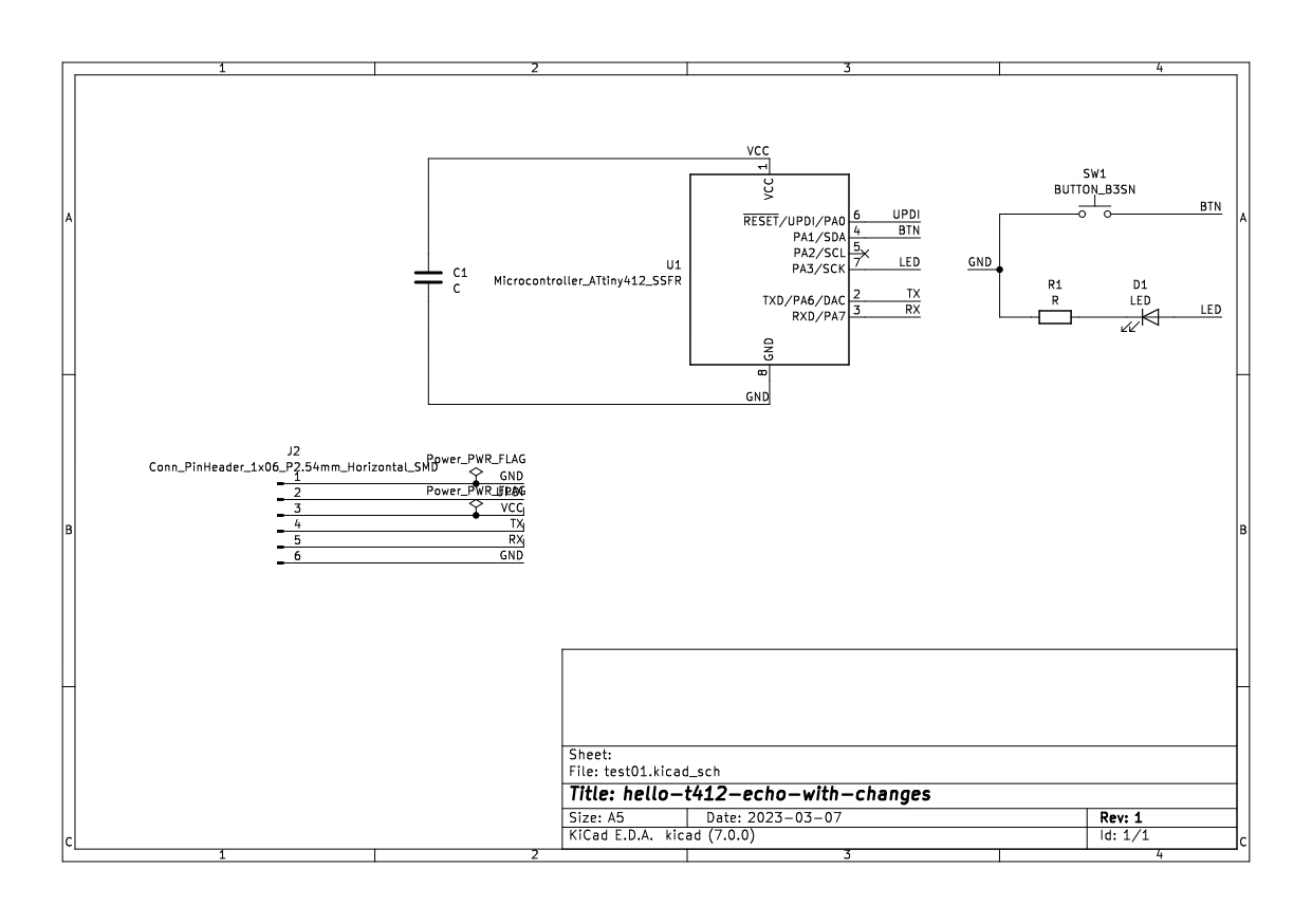
Design Rule Check (DRC)
Here is a brief overview on how to set up the Design Rule Check in KiCad.
Go to "Preferences" and select "Design Rules" or "DRC Rules". In the Design Rules dialog, you'll find various tabs for different design rule categories such as Clearance, Width, Via, etc. Review the default rule values, but if you want to customize them, click on the specific rule category tab and adjust the values according to your design requirements. For example, in the Clearance tab, you can set the minimum allowed clearance between different objects like tracks, pads, and vias. Once you have adjusted the rules, click on the "Check" or "Run DRC" button to perform the Design Rule Check. KiCad will analyze your design based on the defined rules and provide a report of any violations or errors. Review the DRC report and fix any violations by adjusting your design accordingly, such as moving components, modifying track widths, or adjusting clearances. Repeat the DRC process until your design passes all the rules without any errors or violations.
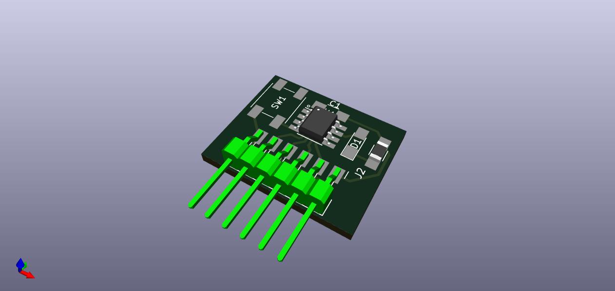
Hero shot - 3D render from KiCAD
After getting used to the workflow in KiCAD I felt confident jumping back and forth from the schematic and the pcb editor. Just like with SVGPCB I enjoyed working in KiCAD and will use it again.
Eagle
Finally I jumped into EAGLE and gave it a try. I got the fab library into EAGLE but struggled to find the components I wanted. I added a XIAO RP2040 microcontroller, some pins, an LED, resistor and a button. I found the workflow to be a bit confusing and not intuitive at all. I managed to get the connections I wanted in the schematic in the end and continued to the board editor. Since this was a pretty straightforward board I did not struggle to route the connections.
I must say I was a little underwhelmed after trying EAGLE, I was expecting it to go a lot smoother but I spent way too much time on just getting used to the workflow.
After trying SVGPCB, KiCAD and EAGLE I would say KiCAD is my favorite, followed by SVGPCB. I was disappointed in EAGLE but maybe I just need to spend more time getting used to the workflow. But I will probably be using KiCAD more in the future.
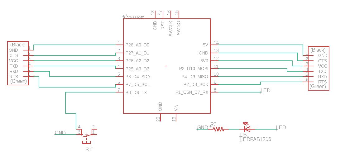
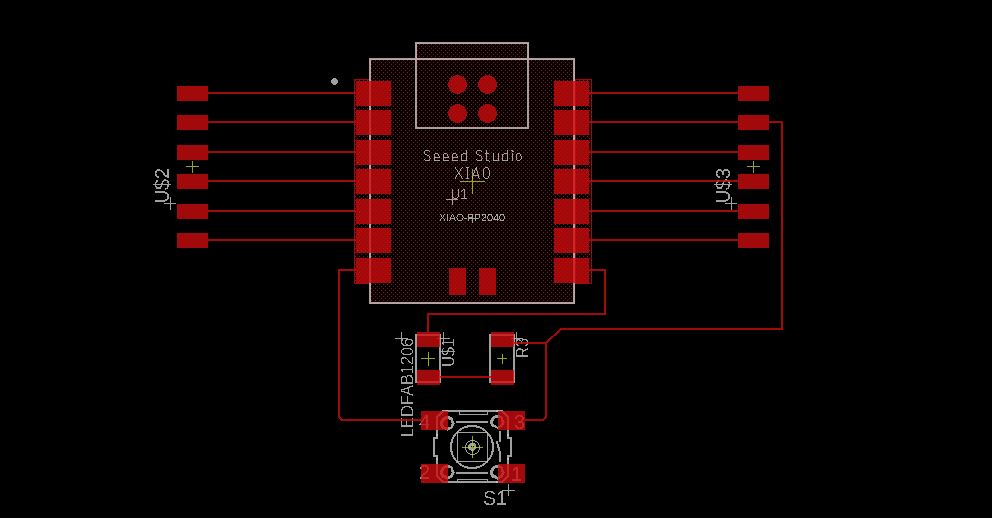
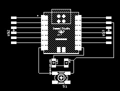
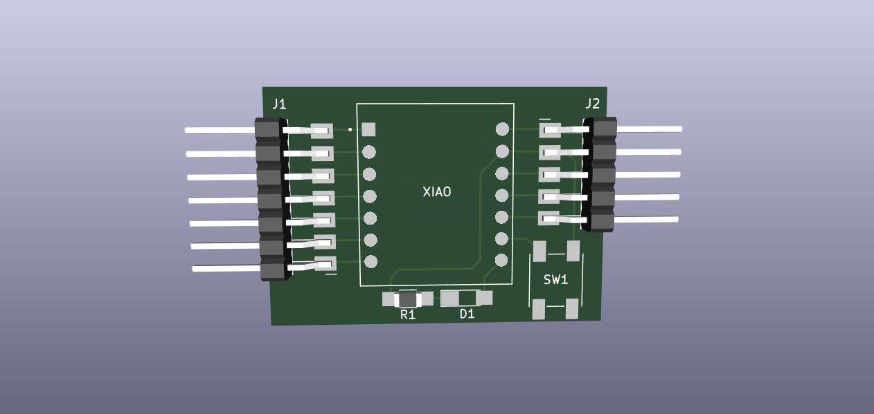
I wanted to play around some more in KiCAD, this time working with a XIAO board. I had to go through the SnapEDA website to find the schematic and footprint for the XIAO board. I routed the pads to some pins and added a button and an LED with a resistor. I found it so much more intuitive working in KiCAD than EAGLE. The hotkeys just make sense and if I ran into an issue it was always easy to figure it out.
Group Assignment
Use the test equipment in your lab to observe the operation of a microcontroller circuit board
For our group project me and Hafey used the test equipment in our lab to observe the operation of a microcontroller circuit board Link to group assignment..