7. Electronics design
This week we started learning more about creating our own PCBs (printed circuit boards). We learned how to use the software KiCad to create a schematic and a diagram for the layout. There was a LOT to learn, but the electronics stuff is starting to make more sense. Still lots to learn.
Goals for the week
- Linked to the group assignment page
- Documented what you have learned in electronics design
- Explained problems and how you fixed them, if you make a board and it doesn’t work; fix the board (with jumper wires etc) until it does work.
- Included original design files (Eagle, KiCad, etc.)
- Included a ‘hero shot’ of your board
- Loaded a program and tested if your board works
Some useful links
Group work
This week we spent some time working on breadboard to understand the basics of how boards should be constructed. I found this very useful because it’s been a long time since I did any physics. Understanding the relationship between resistors, LEDs and buttons was VERY useful for the board design.
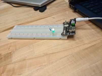
To start with we just set up a simple circuit with an LED and a resistor. Every LED needs a resistor, otherwise too much electricity will flow through the LED and it may very well blow out (or up if too too much!). Jason suggested that we start with a Green LED because it would be brighter than a blue one. We used a resistor of a few hundred ohms (oops, I forgot to write down exactly how many). Here’s an image of our first circuit.
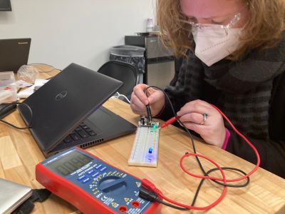
Then we experimented with resistors of different strength to see how they impacted the brightness of the LEDs. More resistance=less brightness. This makes total sense. It turns out that different colors are also different levels of brightness, so it’s not true that one resistance level is the appropriate one for all LEDs. For example we used the multimeter to measure how much voltage passed out of the LEDs given 5V going in. The green one measured 2.34 V after and blue 2.655 V. This now explains why Jason suggested we start with green, which would be brighter. The dropoff of voltage is larger, thus the green LED uses more and is brighter.
Here’s an image of me measuring the voltage on either side of the LED using the multimeter.
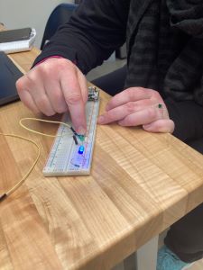
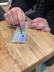
After we experimented with LEDs, we added a button. This was fairly straightforward. The goal was to make sure that there was a complete circuit (hello math - graph theory circuits are the same as electronic circuits here) so that all the components were connected and were powered.
Here are 2 images. In the first the button attached to the green LED is not pressed and then in the following image it is. You can see the light go on!! Whoo hoo… overly excited to make circuits and understand basic physics.
Later when we were designing our own boards I relied on this exercise. It was helpful, but then it also differed in how we wanted to attach buttons in the circuits we created. In our own board we now had to connect them independently to the ATtiny so they were powered separately. In our boards they actually don’t yet interact with the LED since we have not yet programmed our boards yet (still to come in 2 weeks). But now I understand much more about the basics of how capacitors, resistors and other components work and what needs to be connected where.
Through this exercise we also learned more about multimeters. When I was designing my board from week 5 I learned a little about multimeters when things went wrong and various people were trying to help me. This week I learned more about how to use them effectively both in trouble-shooting in the board soldering process and in understanding the way electricity flowed through our breadboard design. The 2 main functions we used on the multimeters were to detect if current was flowing between traces or components and then also to see how the amount of voltage was impacted by capacitors, resistors and other components. This was all pretty interesting.
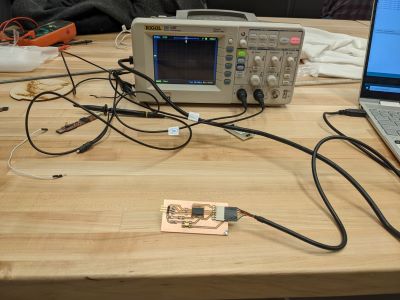
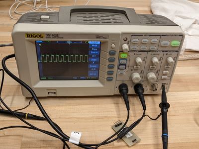
Later Jason also showed us how to use an oscillascope which detects electrical goings-on at a finer level. When my board was programmed we hooked it up to a computer and an oscillascope and were able to see how much finer an instrument the oscillascope was.
Here’s the set up:
Here’s Jason showing us how to use the baseline to check that things are working correctly. See the wave on the oscillascope screen that shows the test signal.
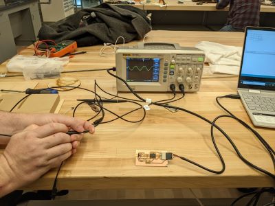
He also showed how to change the settings on the output by testing the electrical flow in the room by putting the test stick to his finger. Look, Jason has electricity!! Or does he…
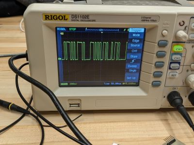
Finally we hooked my board up to the oscillascope and we were able to watch the ascii code that was sent from the computer to my board - how cool is that!! Sarah typed “hello” and then we pulled up the ascii code and checked out how the zeros and ones compared in the wave. SO COOL!!!
KiCad and Board Design
After experimenting with equipment in lab, Jason and Spencer introduced us to KiCad to design our boards. This was super interesting and not too challenging to get to work once you understand how the actual physics stuff works (still working on this).
Jason helped us with the basics that were necessary before we got to the LED and button. We were then to determine that part on our own. This lead to all of us having different models with similar components, part of the point of this week’s homework.
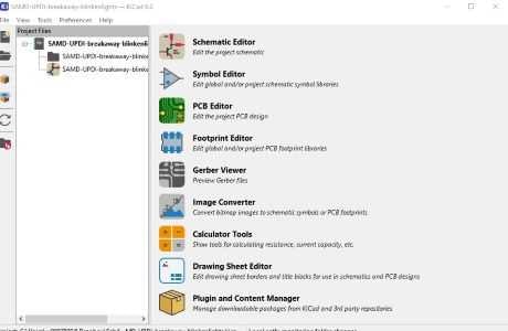
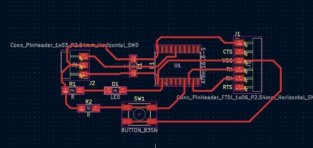
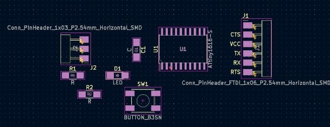
The main things to note about KiCad are that you have 2 interfaces that you want to go between as you’re designing. There was the schematic in which we placed and arranged all our components and then the PCB editor where we placed the components and added traces for the actual board design.
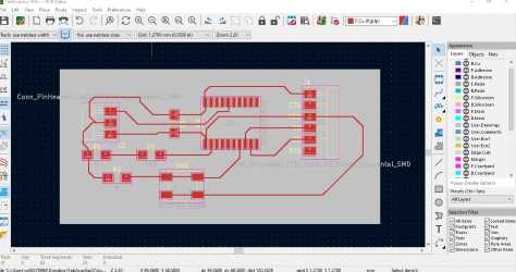
Here is what the main page looks like. YOu see the schematic editor at top and then 2 down the PCB editor.
Jason led us through the basic steps of starting with a schematic and then turning it into a PCB output. You can see a couple of steps in the images below on the PCB layer. It should be noted that the program communicates through the layers and our job was to move the components in the PCB layer so that the placement made sense and so that we could add traces between the relevant components without crossing (hello planar graphs!!).
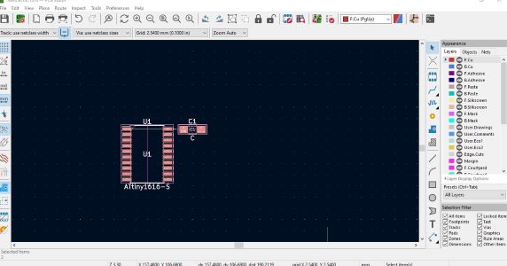
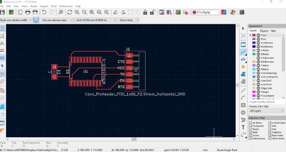
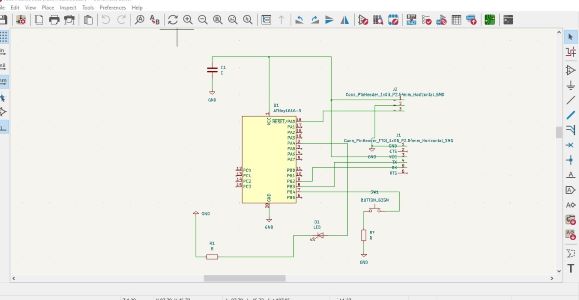
Below are the final schematic image and the final layout for the traces of the PCB:
Before we finished we needed to add the outer rectangle for the board. Note: we were told we could be creative here and design whatever shape we wanted. I just wanted a working board and this is my first time with all of this, so I kept it simple. We had to add a rectangle to the User1 Layer. Note: all the components and traces had been placed in the F.Cu layer (at the top of the layer list).
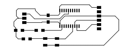
Finally we needed to export the traces and the outline. We did so just using the Export command under File in the menu. You want to make sure you save as an SVG file. You should get 2 different ones - one for the traces and one for the outline. Below are images of both.

One of the files that had good directions for some of the options in KiCad (edge width, etc) and converting your KiCad into SVG files was the google doc Jason prepared for us here for the Roland Mill. I used the Sainsmart one again since that was the one I had used in our previous assignment and I was comfortable with it. There was a version for Sainsmart too (minus the SVG part, so see above for that)! Here it is. Thanks Jason!!!
Milling
To get from KiCad to a physical board we used MODS again. I had to remember to invert the image and then check the settings for both the traces and outside of the board. The output from MODS was the .nc file that I could use in Candle to mill my board.
Here’s a screenshot mid-MODS for the traces. One thing I ran into was that my board wasn’t all getting input/output. I found out (thanks Jason) that MODS doesn’t play well with Firefox, so I switched to Microsoft EDGE and problem was solved.
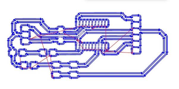
Also, here’s an image of the plan for the mill. I love these outputs bc you can see how many times each line will be gone over by the mill. I think the red lines indicate where the mill picks up and moves across the board without cutting.
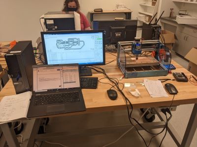
With the .nc files in hand I moved to the computer hooked up to the Sainsmart mill and used Candle to set the mill to go. Here’s an image of the whole setup while milling. You can see I had my own laptop and lots of mouse(s) around. Ugh. I need a better work flow.
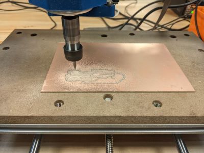
Here’s the mill at work cutting my board.
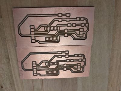
After the first time through cutting my board I realized that I had my traces set at half the width that they should be. I used the multimeter to check to see if the traces were too thin in places, but the connections all seemed ok.
I got paranoid though since my board from 2 weeks ago didn’t work. So I took the time to go back into KiCads and thicken the traces. I googled and found a way to change all the traces at once, which was great since I thought I was going to have to redraw them.
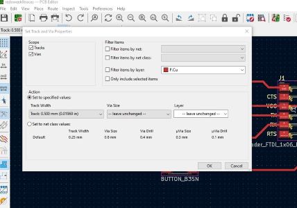
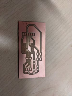
Here are the boards together and you can really see the difference that using a good trace size makes. Noted.
Board components and soldering
We used the ATtiny1616 in our boards. There are continuing supply chain issues and this was a microprocessor that we had and that the instructors said worked well.
The complete list of components that I used:
- ATtiny1616
- red LED
- 1 uf Capacitor
- A button
- 499 Resistor on LED
- 10k Resistor on the button
- UPDI 3 pinout
- FTDI 6 pinout
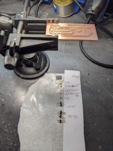
I learned from looking at other Fab Academy pages that one way to assemble components for soldering is to lay them out on double stick tape. This is my version of that. It actually worked great to organize my parts and to have everything ready to go.
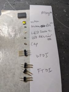
Here was the “map” for attaching the pieces.
I checked both the orientation of the ATtiny, looking at the pinout, and the LED. I was very careful this time since I had to redo both in the first board I made.
Here’s the board and soldering set up.
Last time I used solder paste to solder and had a hard time with it and had some solder bulges on the board several times. So I decided I would switch to using the solder pen and wire. That was a terrible idea! In soldering you have to put solder down on mutliple pads in order ot put componenets down. For instance, the LEDs, resistors and capacitors have 2 pads, the button has 4 and the ATtiny has 20! After putting the solder down on one pad and moving on to the next, the solder hardened!! So I found it very hard to attach components. I will go back to paste!! I did also have a solder mess under the ATtiney and had to redo that part.
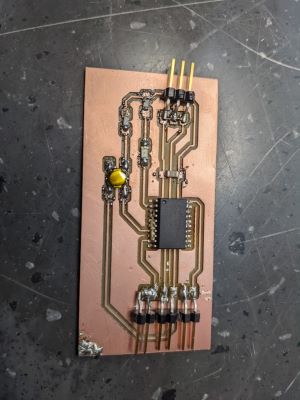
Here’s my finished soldered board:
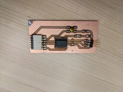
Once I finished this I was not really happy with the FTDI end. We didn’t have any “male” 6-pin headers that I could use so I used pairs of them and needed 3. By the time I got to soldering the last pair, they were really not straight and not attached where they needed to be. Also, see the grossness of the solder. So I used a “female” pin header and then attached a converter (is that what it is called?). So here’s my second “done” board with the components that I kept. I did have to go back and fix some other soldering issues bc things were going to short (according to our TA Tuna).
Programming the board
Once the construction of the board was done I used the Arduino IDE to program my board. I followed the directions from Jason’s Google doc here. The actual programming directions are found in this doc.
Though we added a button and LED we are not actually programming those to work yet. Instead we’re just demonstrating it works with a “Hello Echo” code from the Fab Acaedemy website. I used this.
We had used the Arduino IDE last time, so I had that program on my computer. I needed to use Spencer Konde’s megaTinyCore Arduino core.
My board was connected to my computer using a standard FTDI USB-to-serial cable. I also had to use a converter board since the FTDI cable needed to be converted to UPDI. Fortunately there was one already constructed and was attached to one of the cables in the Lab that I could use.
The directions to install the megaTinyCore are in the file from Jason, but I’m pasting them here with my edits so I can find this again:
Instructions on installing megaTinyCore are here
- Open File / Preferences in Arduino IDE
- Add http://drazzy.com/package_drazzy.com_index.json to the list of “Additional Board Manager URLs”
- In the Tools / Board menu, choose “Boards Manager…” Find megaTinyCore and click “Install”. This may take a while.
- Close the Board Manager.
- In the Tools / Board menu, choose “megaTinyCore” and pick the particular microcontroller you’re using.
- In the Tools / Programmer menu, choose “SerialUPDI SLOW - 57600 baud, any platform, any adapter)”. This option only appears when you have chosen a megaTinyCore microcontroller.
Note you haven’t actually programmed your board yet! You still need an Arduino sketch. I went back to the program from Neil found here and pasted that into the Arduino IDE screen.
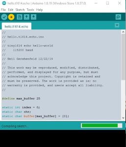
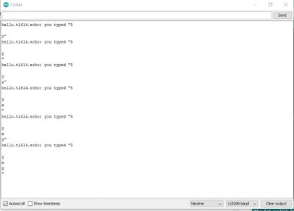
Then I clicked on “upload using programmer” on the sketch window. I watched as the code was compiled and finally it worked!! There were no error messages, so I held my breath as I went to test the programming. As you can see in the screenshot, It worked!!!
Files
- KiCad schem file for my board
- KiCad pcb file for my board
- SVG file for traces
- SVG file for outside
- .nc file for traces
- .nc file for outside