Electronic Design
Redesign Hello-World board
Part of learning to design electronics is getting familiar with tools that are used by redesigning one of the hello world boards. I’m new to using them myself, but had a lot of projects where it was used by my colleagues from the electronics engineering department. Most frequent I came accross Orcad.
KiCAD vs Eagle
For my own use I did have a look into Eagle first. This application is now from Autodesk and integrated in Fusion. Biggest advantage is that it can generate a 3D model you can use directly in your 3D design. Unfortunately it had a limited library available. Probably you can add others, but I didn’t want to go through that quest yet and looked at KiCAD first.
KiCAD was already installed during our bootcamp week. The interface is quite intuitive and easy to learn. I have already some basic knowledge of electronic schematics which makes drawing my schematics not very difficult.
Schematics
We had instructions which components to use and had to redesign the board with the right connections and values. One way of drawing schematics is the “global label” method where you connect components by addressing them with a label. For complex boards that’s very convenient, because you can make a lay out that is independent of the connections between the components.
Because the ATtiny412 board is very simple I used the schematic method using lines between the connections. Advantage is that it gives you a better understanding of the way the circuit works and of the coherence of the board. Here’s a screenshot of the schematics.
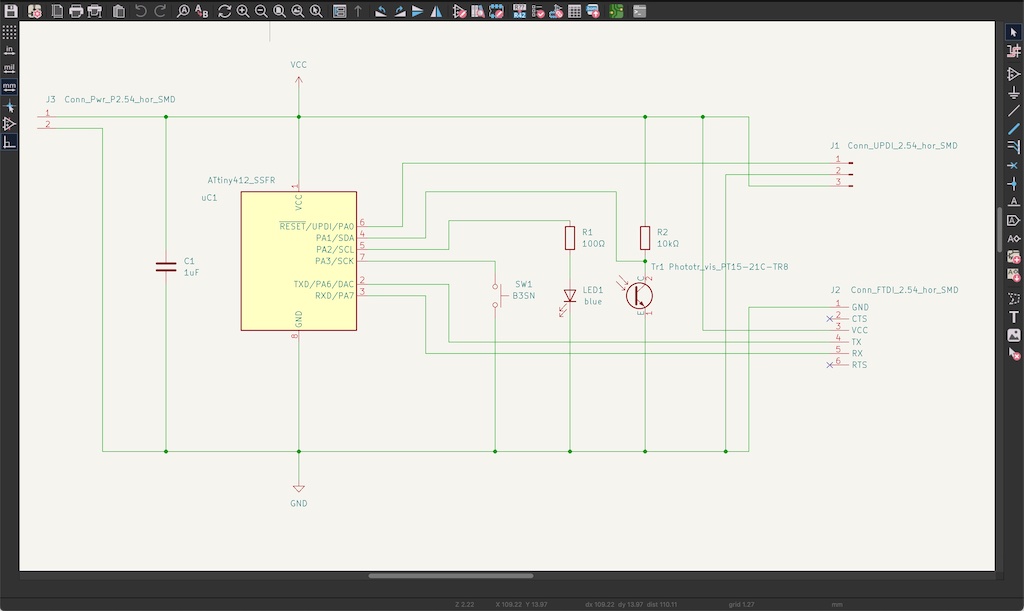
And here’s a list of used components:
| Reference(s) | Value | LibPart | Footprint | Datasheet |
|---|---|---|---|---|
| C1 | 1uF | Device:C | Capacitor_SMD:C_1206_3216Metric_Pad1.33x1.80mm_HandSolder | ~ |
| J1 | Conn_UPDI_2.54_hor_SMD | fab:Conn_PinHeader_1x03_P2.54mm_Horizontal_SMD | fab:PinHeader_1x03_P2.54mm_Horizontal_SMD | ~ |
| J2 | Conn_FTDI_2.54_hor_SMD | fab:Conn_PinHeader_FTDI_1x06_P2.54mm_Horizontal_SMD | fab:PinHeader_FTDI_01x06_P2.54mm_Horizontal_SMD | ~ |
| J3 | Conn_Pwr_P2.54_hor_SMD | fab:Conn_PinHeader_1x02_P2.54mm_Horizontal_SMD | fab:PinHeader_UPDI_01x02_P2.54mm_Horizontal_SMD | ~ |
| LED1 | blue | Device:LED | Diode_SMD:D_1206_3216Metric_Pad1.42x1.75mm_HandSolder | ~ |
| R1 | 100Ω | fab:R | fab:R_1206 | ~ |
| R2 | 10kΩ | fab:R | fab:R_1206 | ~ |
| SW1 | B3SN | fab:BUTTON_B3SN | fab:Button_Omron_B3SN_6x6mm | https://omronfs.omron.com/en_US/ecb/products/pdf/en-b3sn.pdf |
| Tr1 | Phototr_vis_PT15-21C-TR8 | fab:Phototransistor_Visible_PT15-21C-TR8 | fab:Q_1206 | https://www.everlight.com/file/ProductFile/PT15-21C-TR8.pdf |
| uC1 | ATtiny412_SSFR | fab:Microcontroller_ATtiny412_SSFR | fab:SOIC-8_3.9x4.9mm_P1.27mm | http://ww1.microchip.com/downloads/en/DeviceDoc/40001911A.pdf |
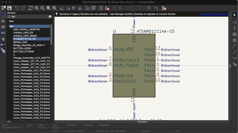
When placing components there are a lot of types and footprints to choose from, but there is a specific library called “fab” that displays the components of the fabacademy invetory. Below is an example of selecting the SAMD from the inventory of our fablab.
Component Values
The values of the resistors and of the capaciter were not give and had to be defined. For the capaciter I just browsed designes from previous yaers and came up with 1 µF. The function of this C1 is to get rid of noise on the Vcc before it is fed to the components and especially the ATtiny.
The resistor from Vcc to Tr1 is to make sure it gets power but that the impedance to the pin of the ATtiny is lower and will swich if Tr1 is activated by light.
The resistor in series with the LED is to make sure that the current through the LED is set to the right value. This one has to be calculated using the datasheets. From them we learn:
- Vfw = 3,2 V nominal
- Ifw = 20 mA typical
- Vpa2 = 5 V
Now we can calculate: R1 = (Vpa2 - Vfw) / Ifw = 1,8 / 0,02 = 90 Ω so we use the closest value: 100 Ω.
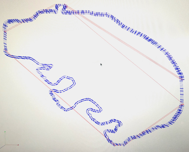
Routing
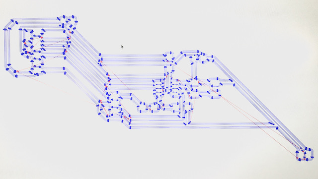
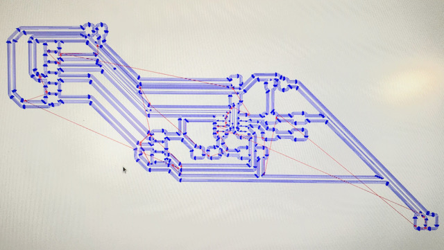
The routing is done manually in the PCB editor. First all components are generated on the board by KiCAD and thin lines represent the connections the way they were made in the schematics. The easiest way I found doing this is to start with Ground, followed by Vcc conections and the rest at the end.
| routing | 3D view |
|---|---|
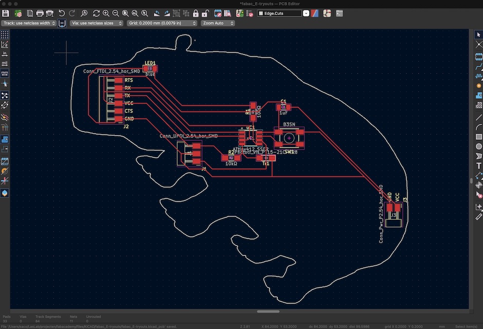 |
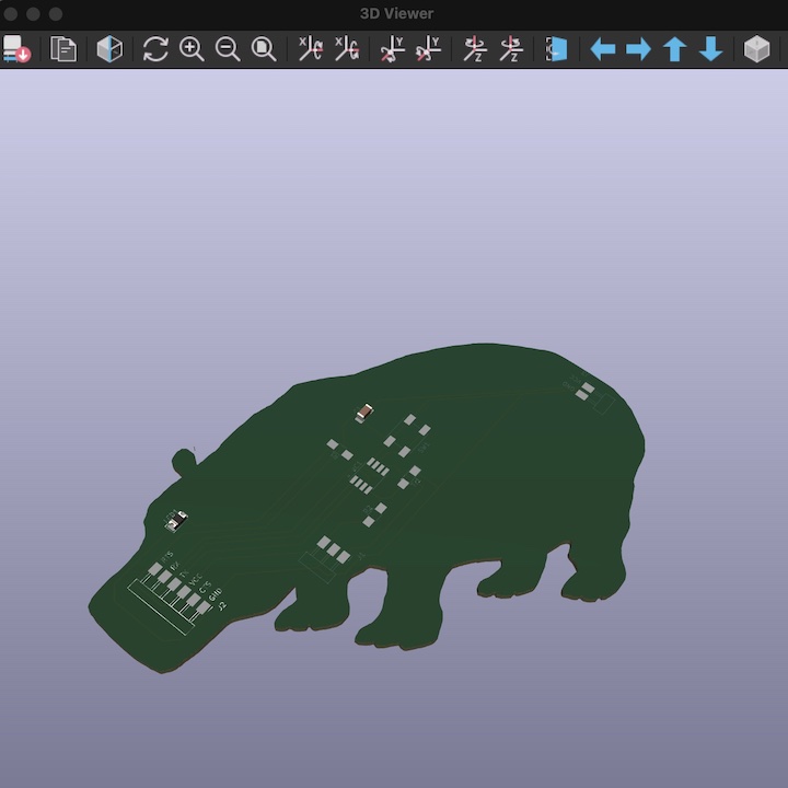 |
Some board setup is needed to comply to the restrictions of our PCB milling machine. The values I used are:
- trace width: 0,2 mm - Henk recommended 0,4 mm but that slipped my mind
- distance between traces: 0,4 - this valu should be large enough to let the default trace milling bit pass
For the total overview of settings there’s a separate section on the overview page:
There’s a Design Rule Checker (DRC) in KiCAD to verify your routing. If I had looked a bit closer to the results I should have seen this line:
Clearance violation (netclass 'Default' clearance 0.4000 mm; actual 0.2073 mm)
Rule: netclass 'Default'; Severity: error
@(148.1800 mm, 81.9150 mm): Track [Net-(J1-Pad1)] on F.Cu, length 2.3759 mm
@(147.5800 mm, 83.1850 mm): Pad 5 [Net-(R1-Pad1)] of uC1 on F.Cu
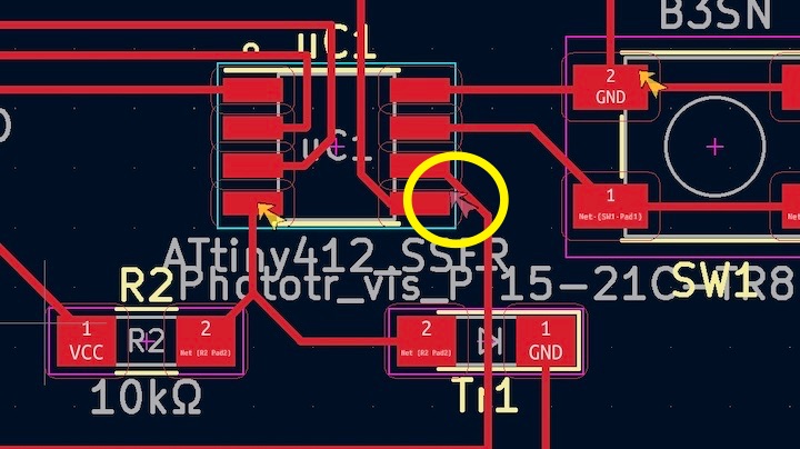
Luckily this error was corrected easily with a knife.
Errors
Of course some issues didn’t go well. Some traces were too close to others or to close to a footprint. Result was that there were errors in the toolpath. Below you can compare the failed and correct traces.
| failed traces | correct traces |
|---|---|
 |
 |
An other issue occured when trying to load the board outline. First the grphics file I imported for the outline to make a second hipp was default placed on a user.drawing layer. It took me some time to find out that in the importpop up you can select the specific layer to use, in my case “edge.cut”.
Secondly there was a strange extra path showing up that wasn’t visible in the svg file in Inkscape. In the end I had to turn to Henk to remove it. He did so using imagemagic to convert from svg into png and I used that as import for mods.
convert -density 1000 -units pixelsperinch fabac_E-tryouts-Edge_Cuts.svg -channel RGB -negate fabac_E-tryouts-Edge_Cuts.png
| failed outline | correct outline |
|---|---|
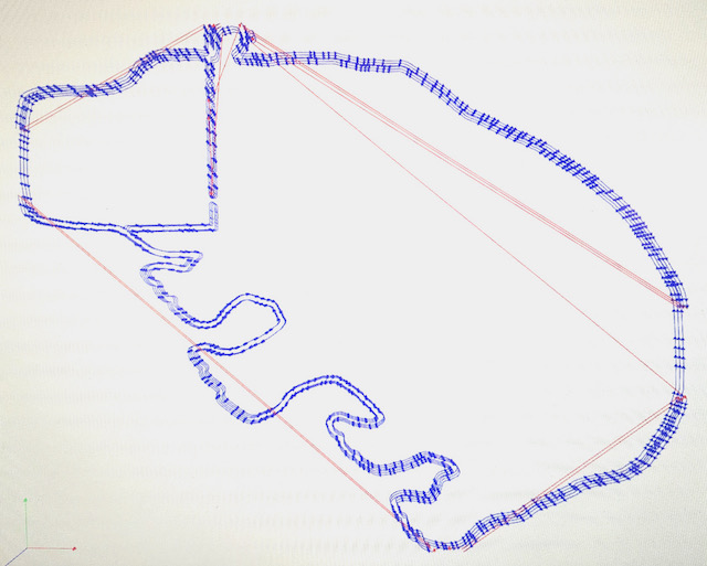 |
 |
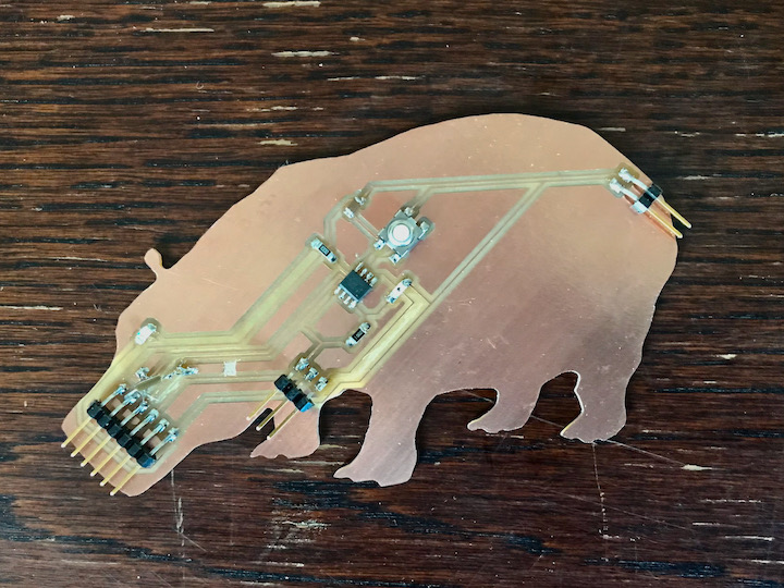
Results
After milling and soldering, this was the result with an optional power connection at his tail and the LED in his eye. Later (see programming) I discovered I had mirrored the serial connector and flipped the Rx and Tx. To solve the latter I made a patch for switching them back.
The design files that were used in KiCAD are located here: