5. Electronics production
Working in group
Extra credit if sent to a company to manufacture the PCB.
While Professor Niels explained the class, we captured the image of the model pattern that interested us.
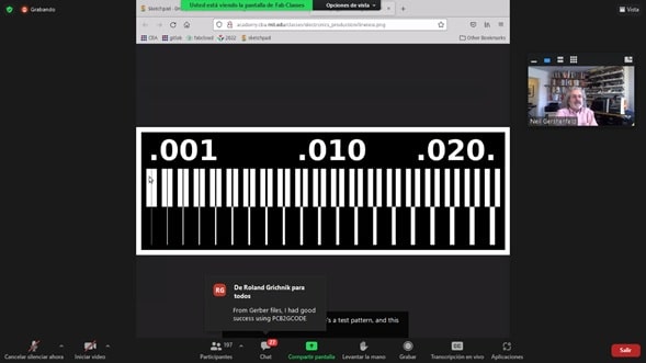
According to the linear test pattern, we search and select references on the web.
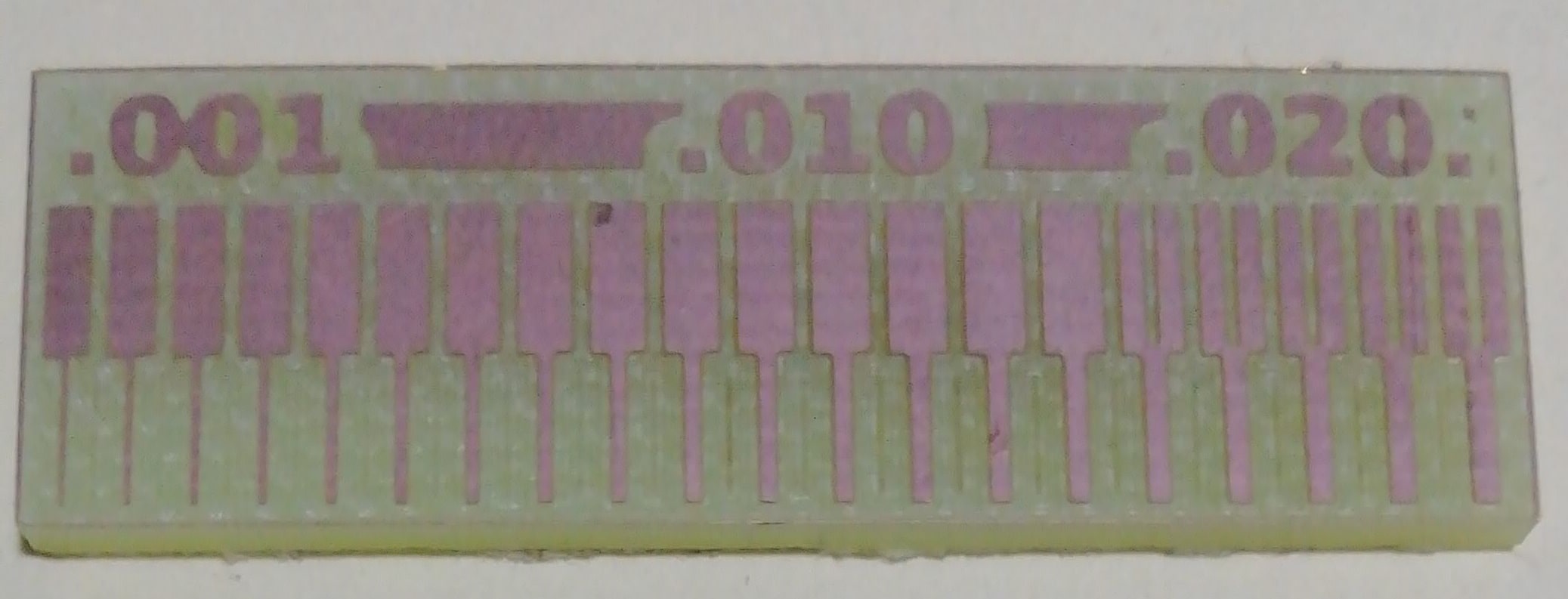
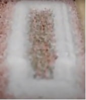
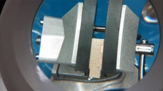
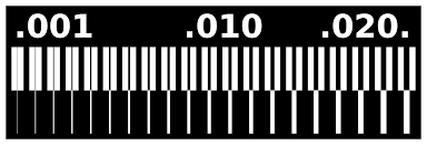
Pattern_Test.png:This is the picture of our in-house PCB production process to test the resolution of the machine.

For reasons of not having the Digital Manufacturing Laboratory, our work is pending to be tested on a CNC machine.
The exploration of the Fabmodule is pending.
Reflection
Unfortunately, due to not having the PCB production machine, the procedures for obtaining the standard printed circuit board have not been carried out, leaving our practical knowledge without any reinforcement.
Note
Once the teams arrived at the IES FPGV, we began to carry out the pending work as of 07-04-2022
Machine
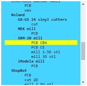
We have one Monofab machine that we have at our disposal. Let's describe the SRM-20 in detail:
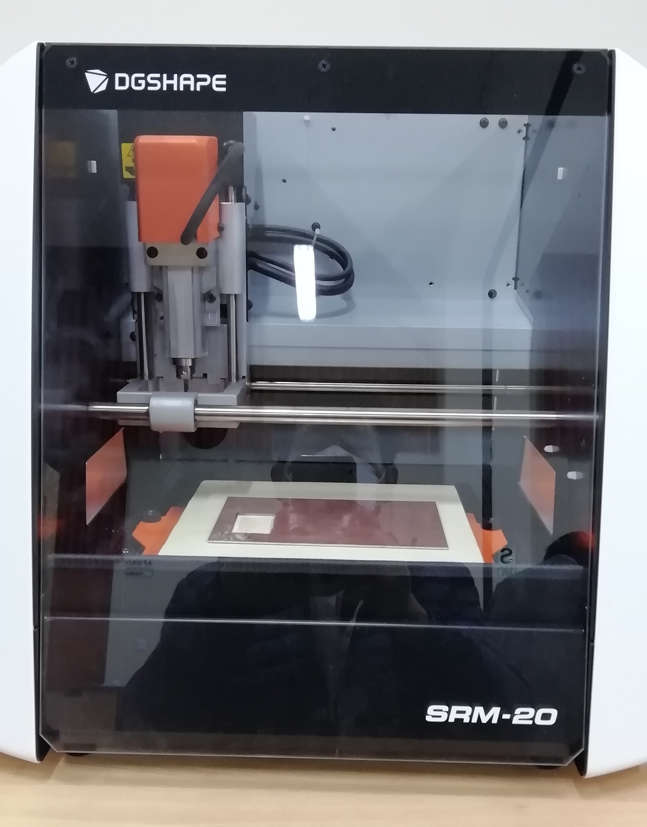
SRM Specifications:
Work area: 203 x 152 x 60mm
Loadable workpiece weight: 2kg
Operating speed: 6mm/min - 1,800mm/min
Spindle speed: 3,000 ~ 8,000rpm
Input Format : RML-1 (.rml)
Material: PCB, Modeling Wax, Chemical Wood, Foam, Acrylic
The tools we have at our disposal are: 1/64-inch cutters for tracing (or scraping) and 1/32-inch cutters for PCB contouring.
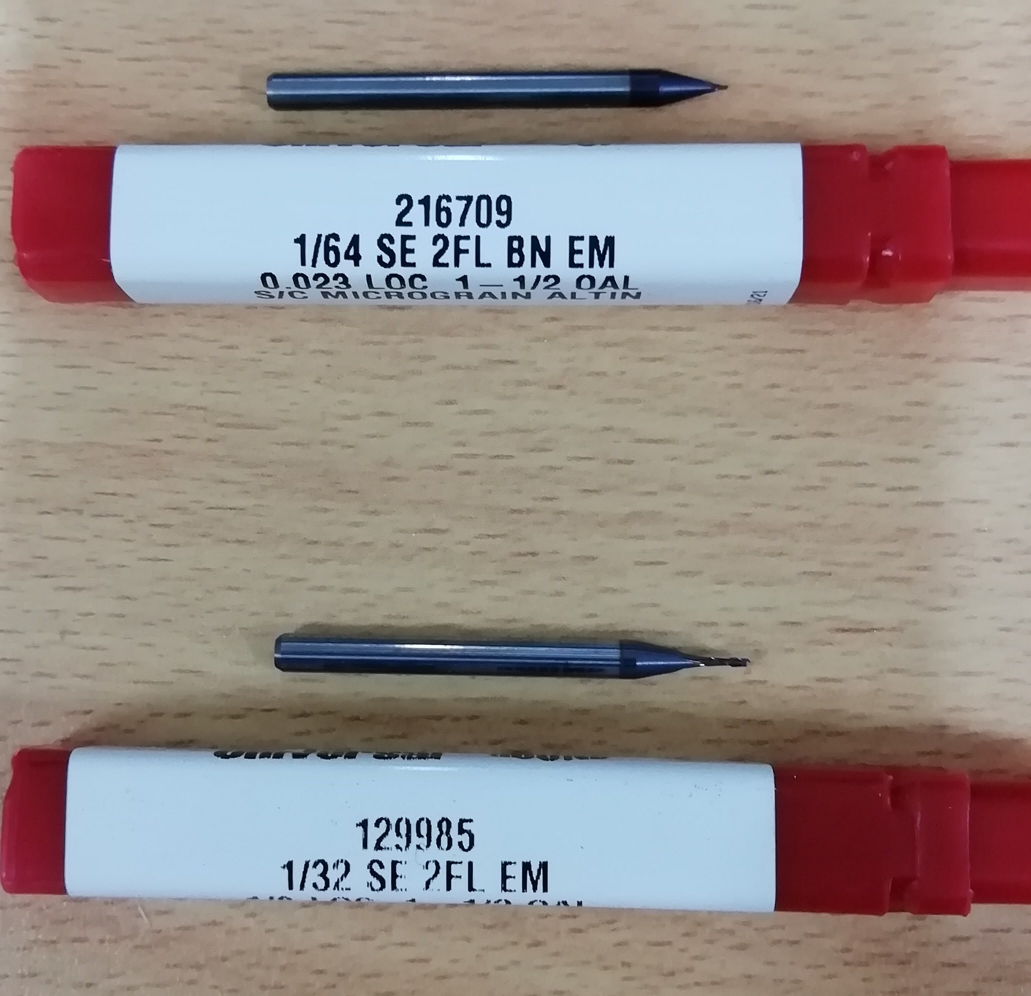
These cutters are the most used for PCB manufacturing with the Roland SRM-20.
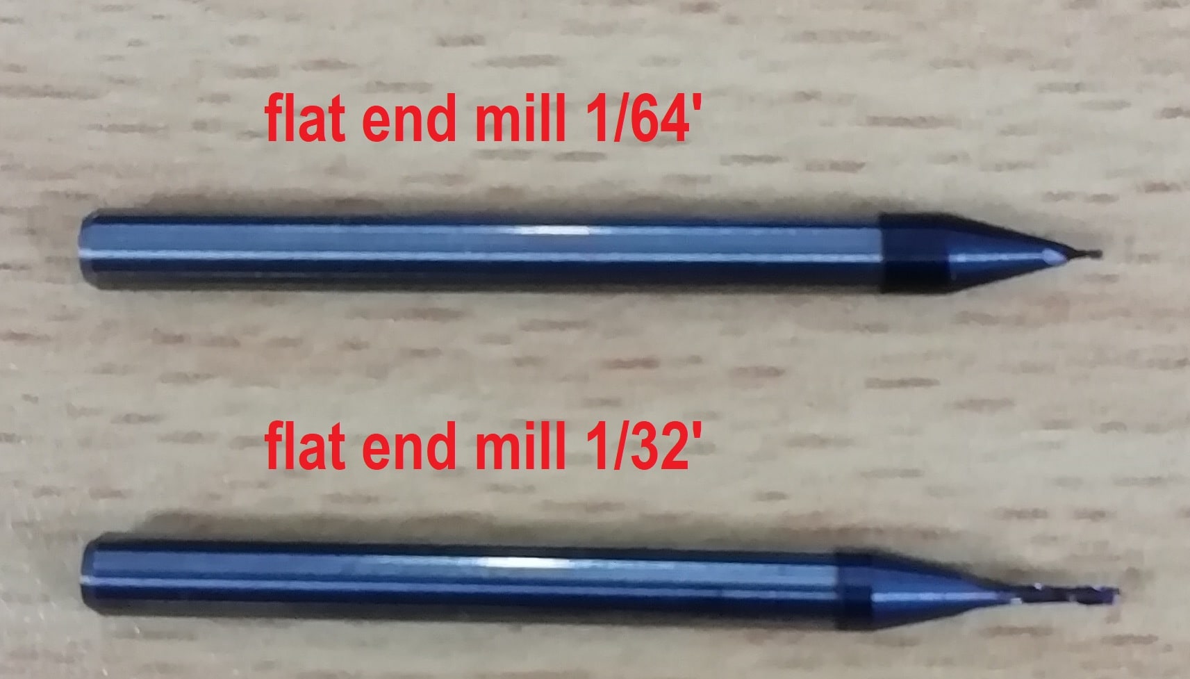
The tip of the bur should not be touched with the fingers and handled with care.
Fab Modules
The fab modules provide a set of software tools for personal fabrication, intended for use with machines common to fab labs.
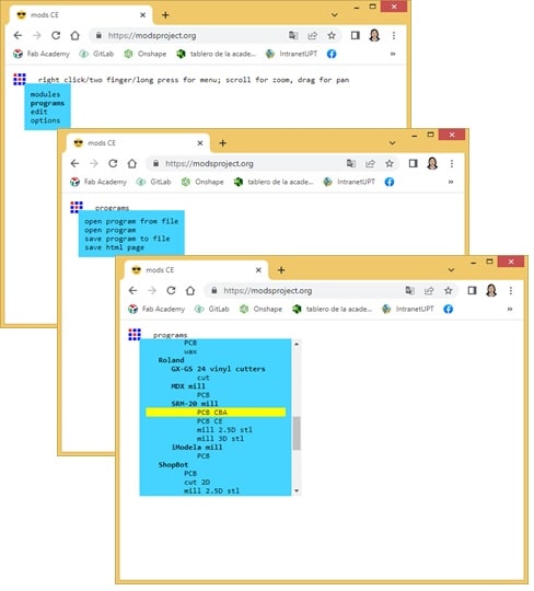
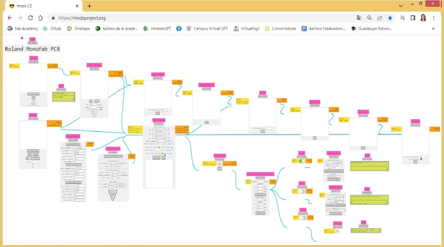
To facilitate the work of creating the PCB, we have the fabmodules and mods to transform from pngs to .rml format that the SRM-20 uses. There are two active links:
a) https://modsproject.org
b) https://mods.cba.mit.edu
In our case we will use the first.
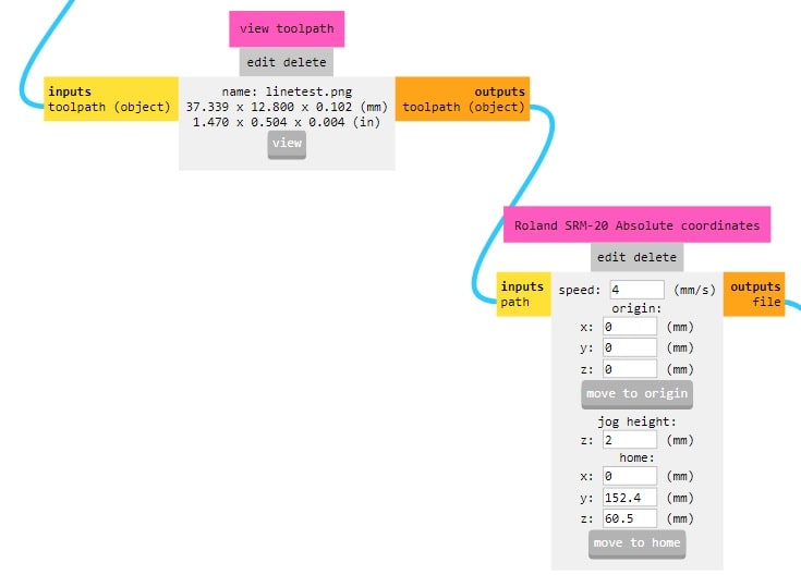
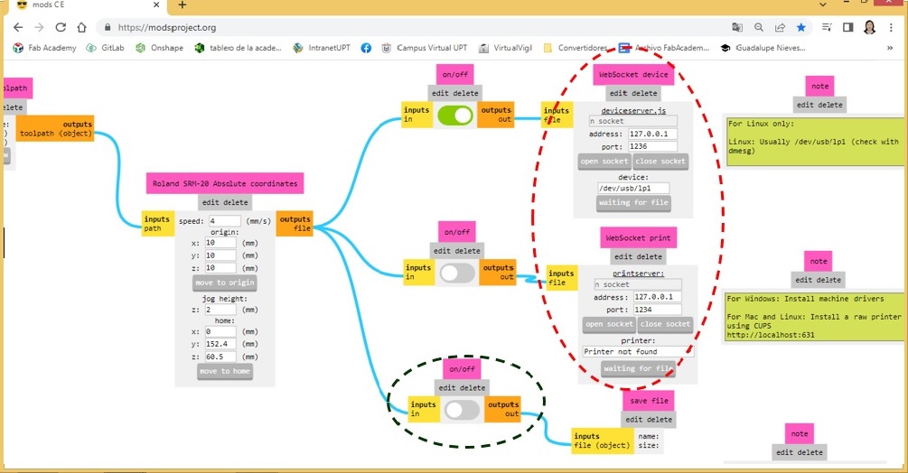
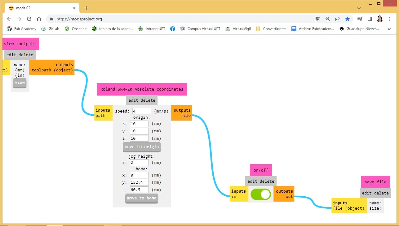
In the mod environment, just open Programs > Open Program > Machines > SRM-20 Mill > PCB CBA. In our case we are not going to network the Monofab, so we delete the WebSocket blocks. We also enable the output to download the generated .rml file
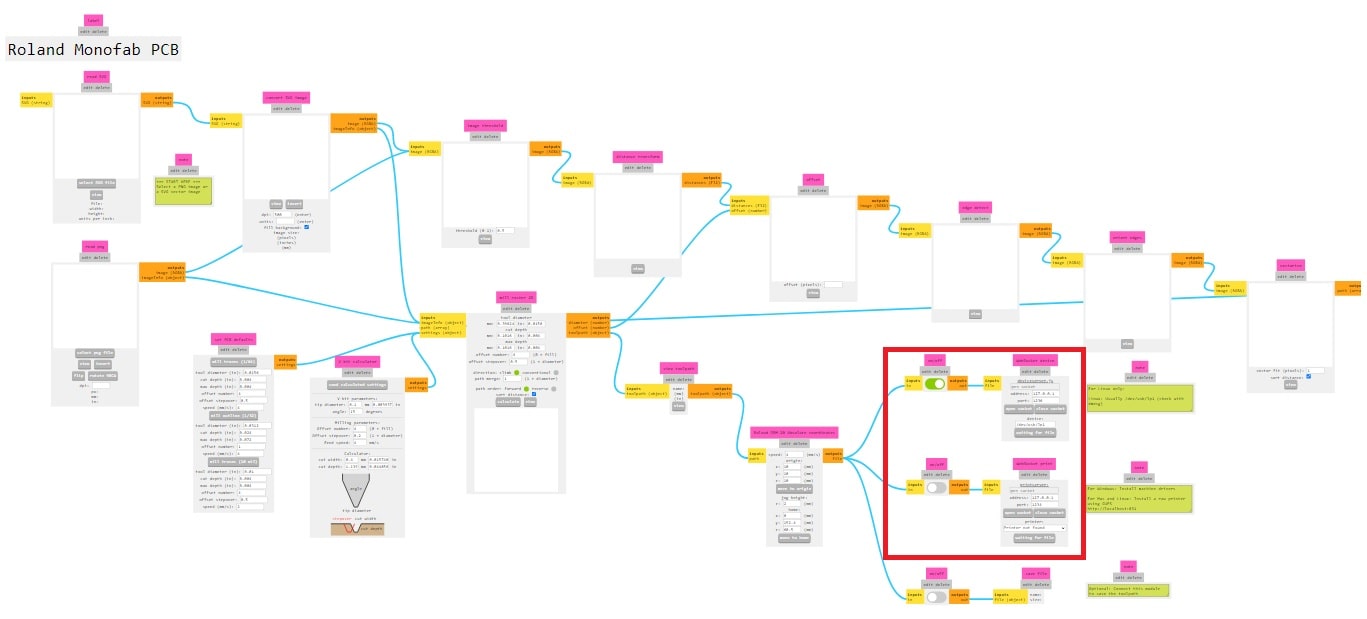
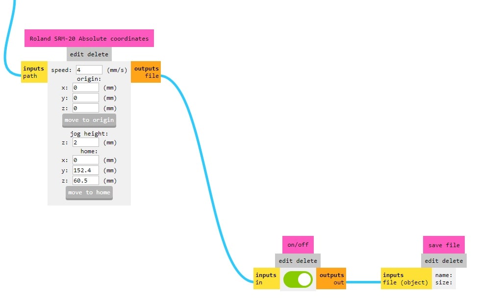
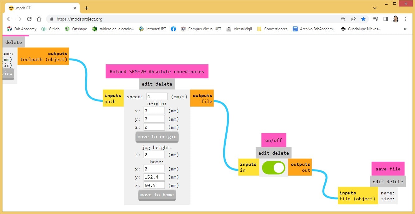
We set the coordinates (x, y, z) to (0, 0, 0) and keep the displacement speed at 4 mm/s, jog height at 2 mm.
Resolution test
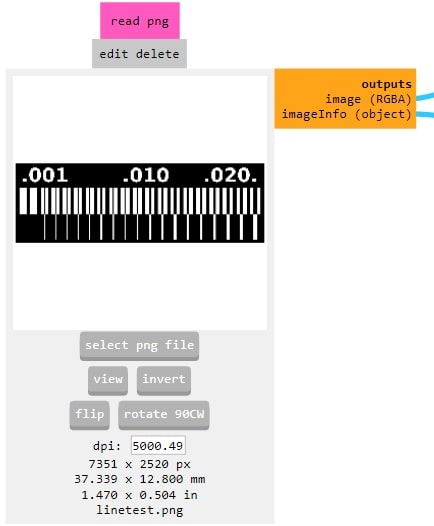
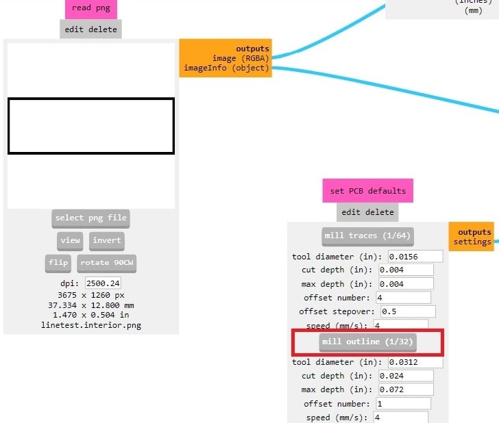
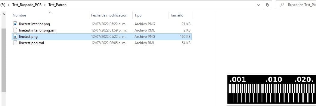
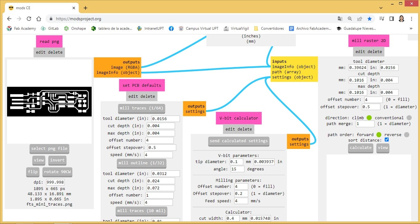
In the read.png block we load the pattern PCB image: linetest.png
For the mill traces we use the default settings of the mods, so we don't have to calculate speeds and depths because they have worked perfectly.
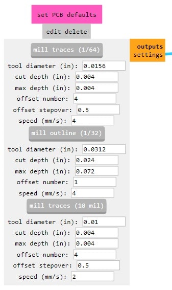
We keep the speed at 2 mm/s and the displacement height of the milling cutter in the air at 2 mm.
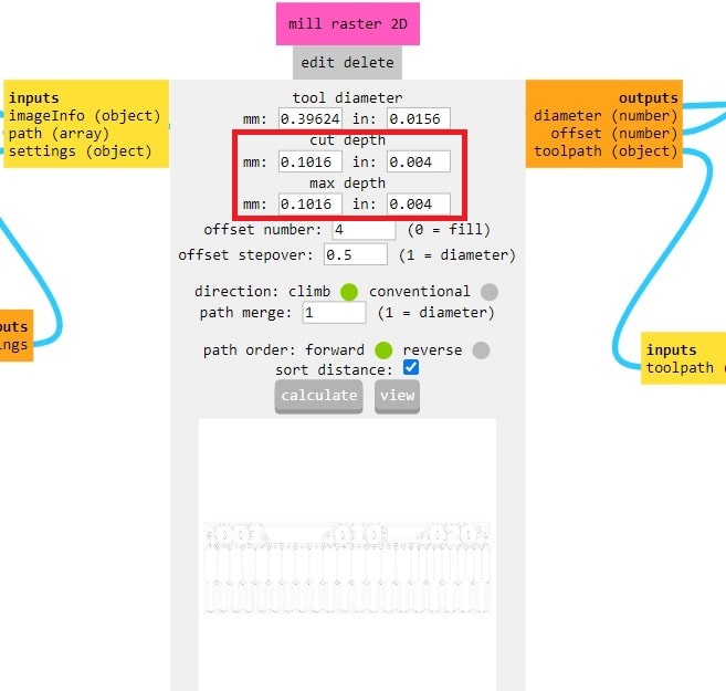
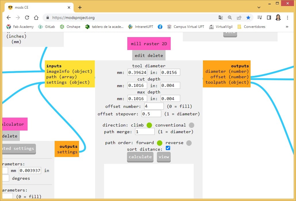
The milling raster 2D block then calculates the cut depth, which defaults to 0.1016mm and the number of passes is 4.
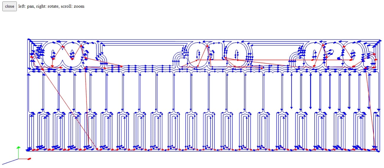
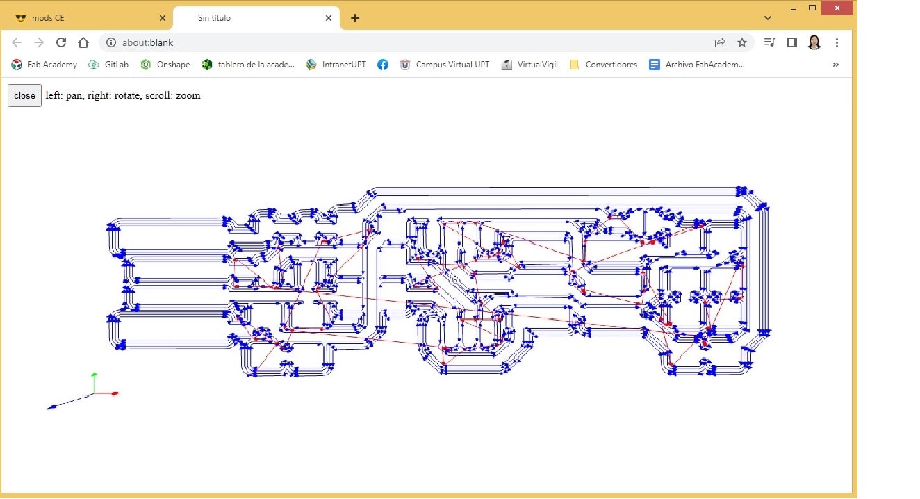
Pressing calculate generates the .rml format that is downloaded to the computer and gives us a perspective of the pieces of the milling machine on the PCB.
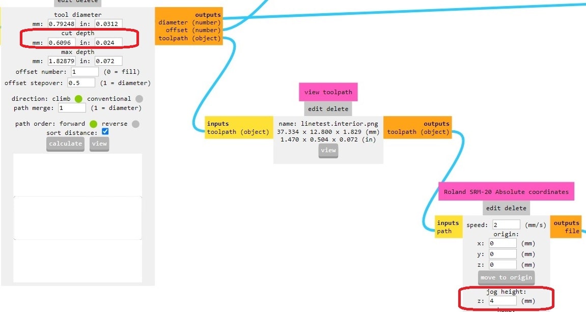
Similarly for the PCB outline, we load the file: linetest.interior.png in the Mods. For this case we have considered a speed of 2 mm/s and a jog height of 4 mm. The depth of cut is left at 0.6096 mm.
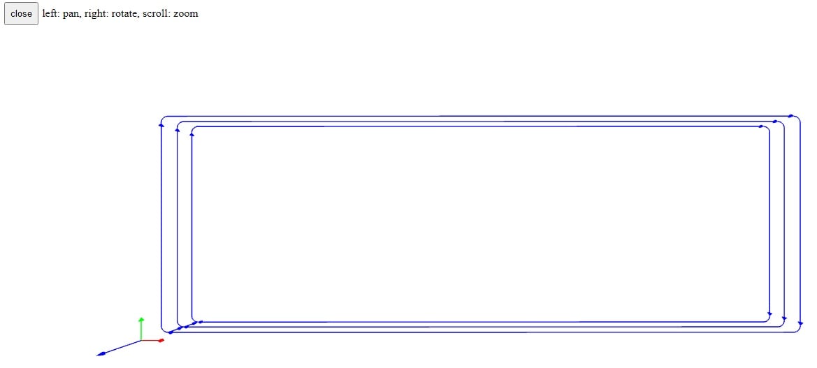
Finally we got the two .rml's files to perform the test. We now proceed to use the Roland SMR-20.
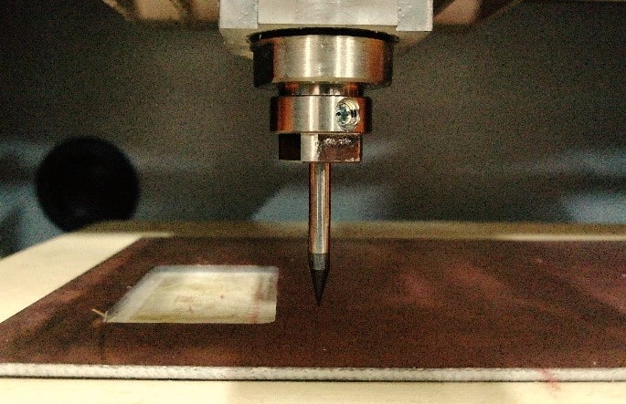
Testing the Monofab with the tolerance test
Calibrating the initial position of work.
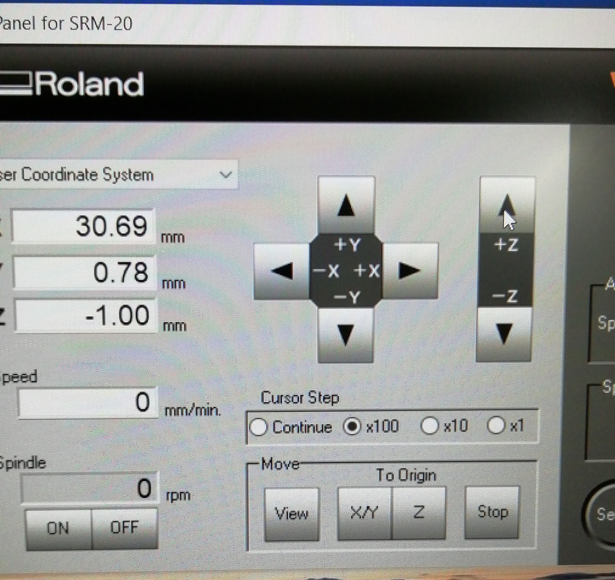
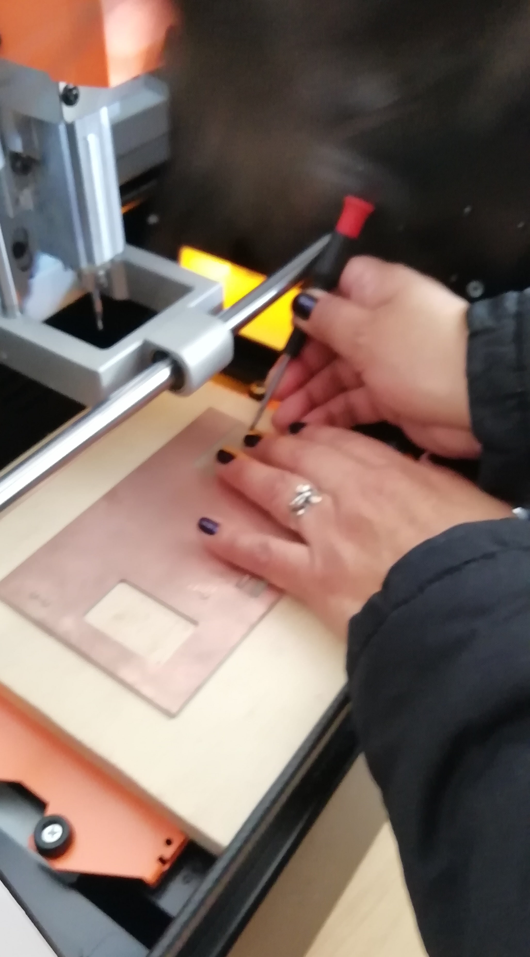
We lower the tip of the cutter holder (Z) to the bottom. Then with the hexagonal tool we loosen and make the dam fall until it touches the PCB. We move up two positions to steps x100. Then we return to adjust the strawberry. In the Vpanel we adjust the positions of X=Y=Z=0. We load the .rml file and the cutting process begins.
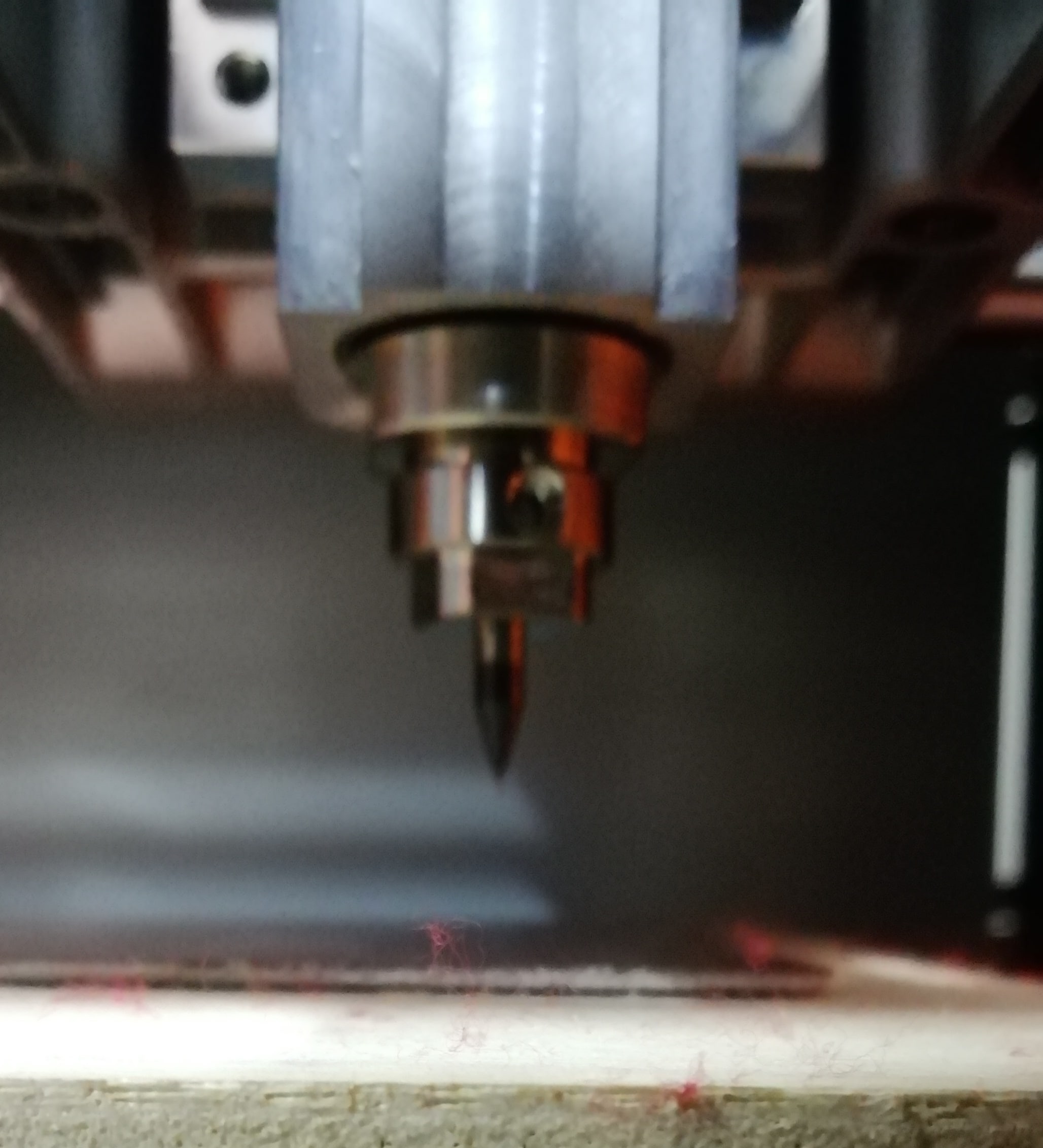
Mill outline process.
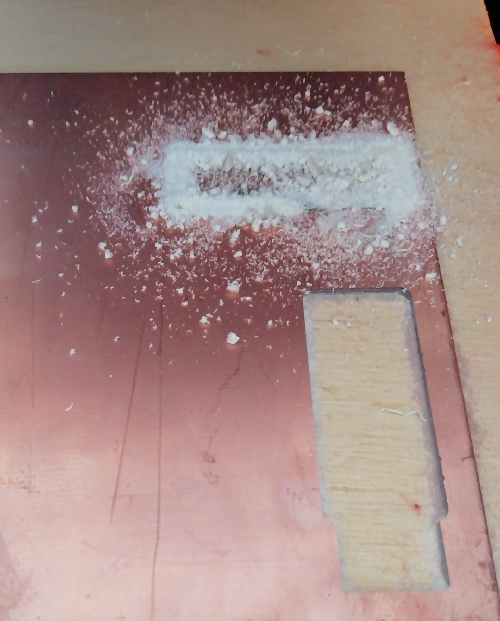
We carry out a cleaning of the detached chip.
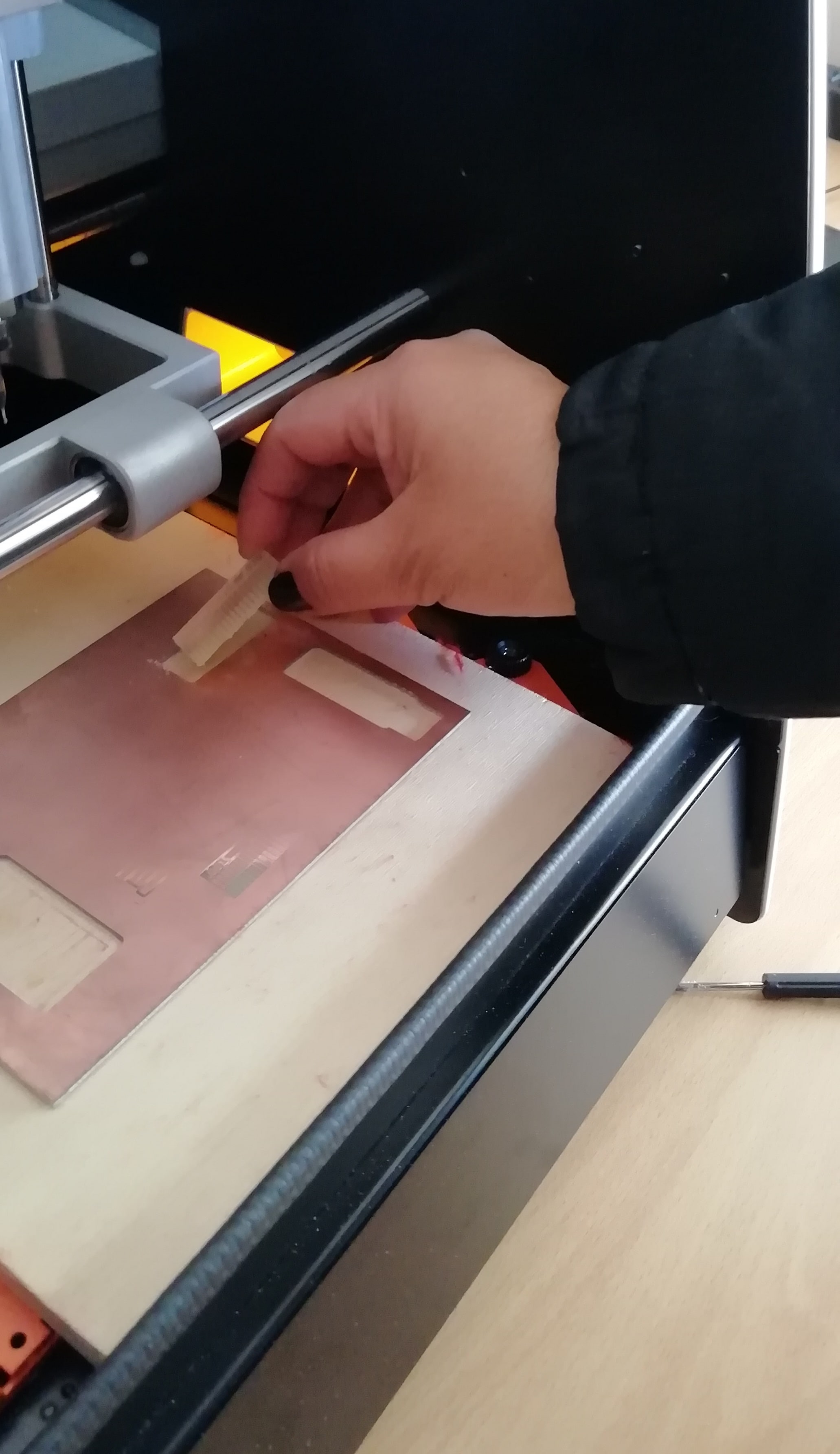
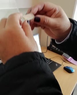
With a small flathead screwdriver, we remove the PCB pattern.
We remove the PCB pattern.
And we have it ready
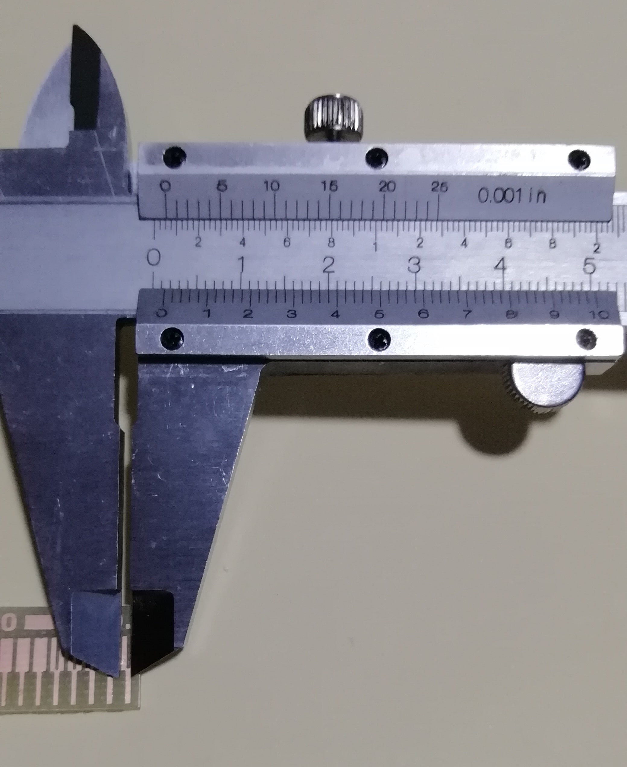
Finally, here we have the test result:
We check the thickness of the track which is 1.38 mm.
What is learned?
Working individually
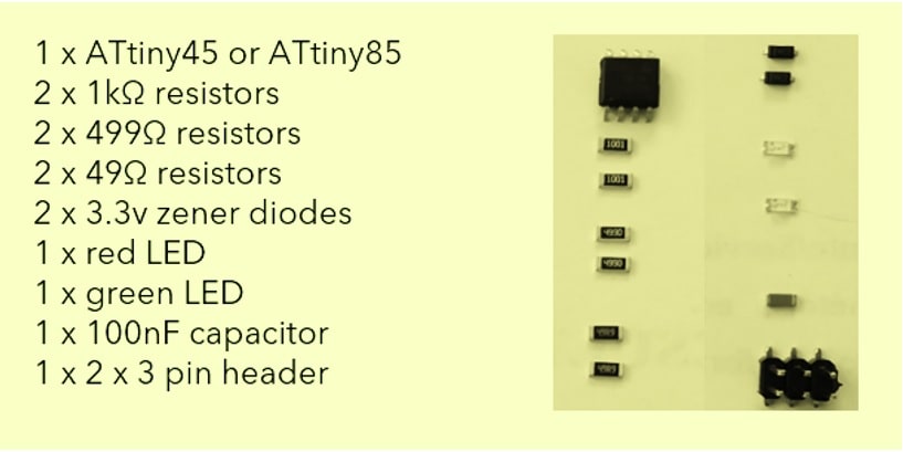
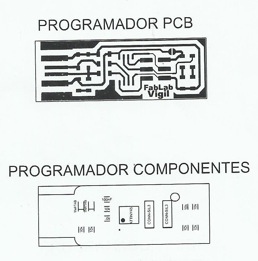
After reviewing different works made by participants, in addition to tutorials from the Fab Academy, I found one that, due to its simplicity, was consistent with my inexperience in PCB design; FabTINYISP “Brian” This is an ISP-like programmer (AVR) in the Attiny85 version.
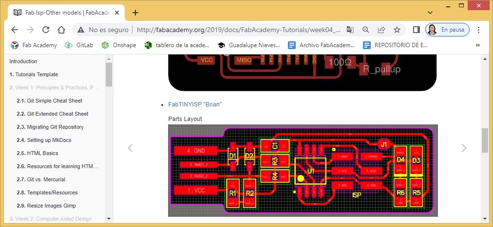
Through the Link "FabTinyISP Brian"it is possible to access the page "Building FabTinyISP", the same one that served as a reference for the development of this work.
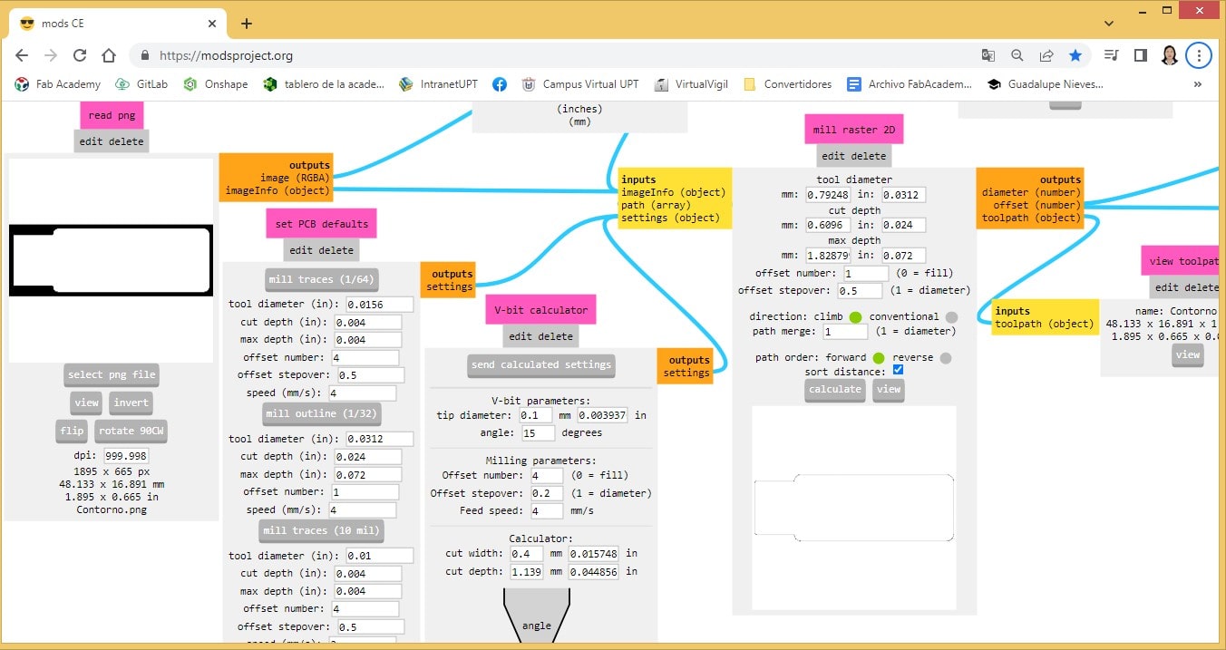
First of all, we proceeded to download the design files: Rastros.png and Contorno.png


In the same way that the group work was carried out, the Fab Modules are used to obtain the files in .rml
The Fab Modules software is loaded online.
With the interface open, context menu/programs/open program/Roland/PCB CBA
Total view, once the Fab Module is loaded.
I proceed to remove the webSocket blocks and activate the output to download and save the generated .rml files.
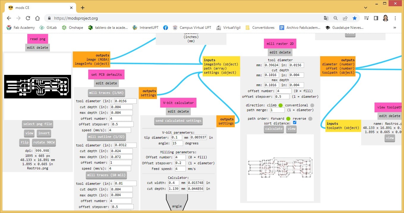
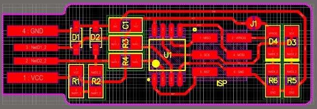
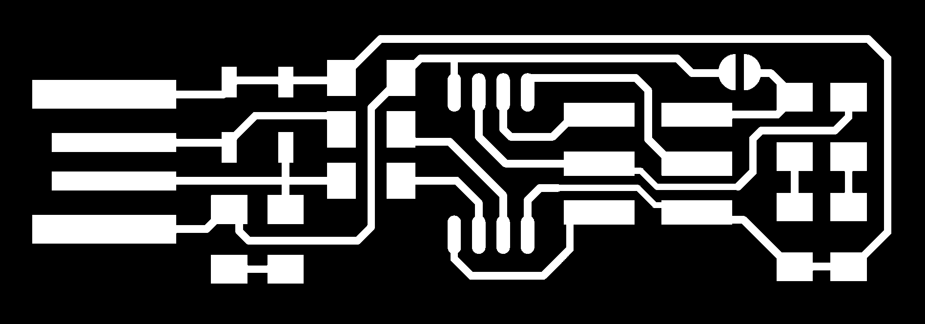
The schema looks like this:
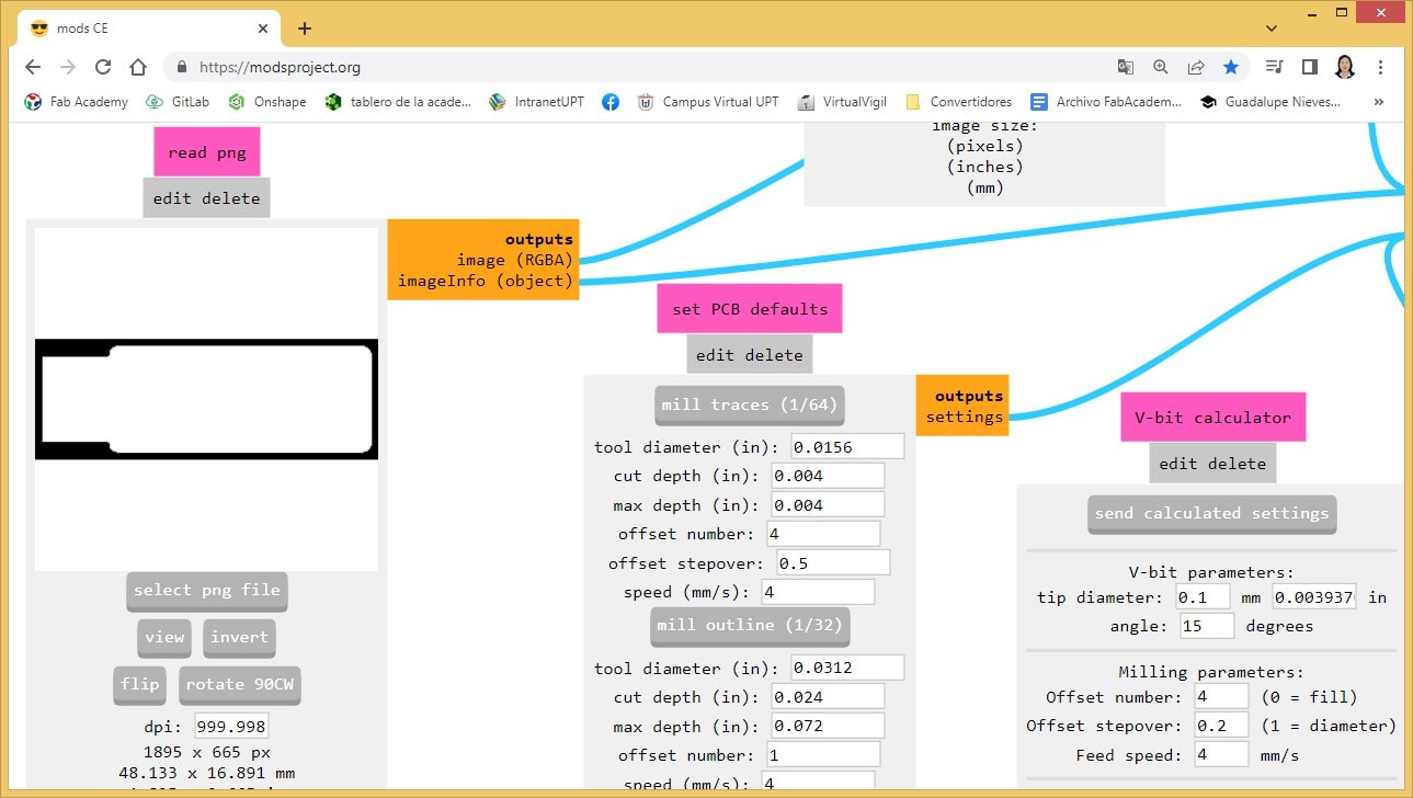
In the read png block (select png file) we proceed to load the file Rastros.png
The strokes will be milled with a 1/64” (0.0156)
In 2D raster mill, the depth of cut is 0.1016 mm and the number of passes is 4.
In Roland SRM-20 Absolute coordinates the coordinates are set to (0,0,0), the speed 4 mm/s and the height 2 mm.
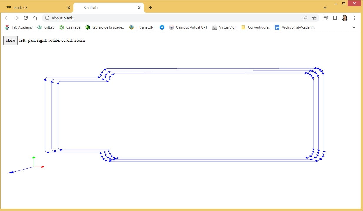
In mil raster 2D, clicking on the calculate button generates and downloads the Rastros.rml file, showing a preview of it at the same time. It proceeds to its engraving, to then close the preview.
The schema finally takes the following form:
The ones prior to loading the contour.png file in the Fab Modules are exactly the same as what was worked with Rastros.png
In this case, 1/32” (0.0312) is chosen as the outline of the PCB, as a reference to the size of the milling bit.
Likewise, the coordinates are (0,0,0). The speed is reduced to 2 mm/s and the height is increased to 4 mm.
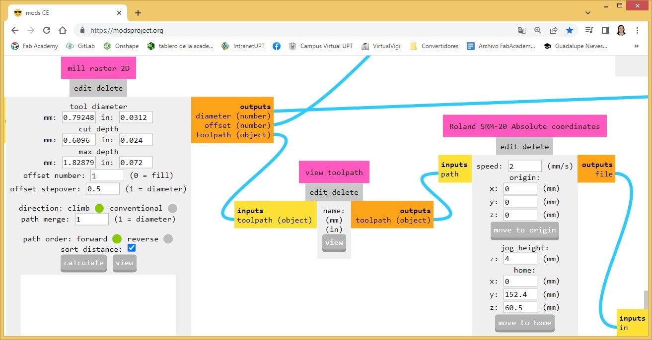
Pressing Calculate it is possible to obtain the file Contorno.rml
The full schematic view looks like this:
PCB Cutaway: FabTinyISP
We proceed to prepare the Monofab SRM-20, for this the reference coordinate (0,0,0) is specified, the point from which milling will begin.
The cut begins.
The cut was made in 2.26 min.
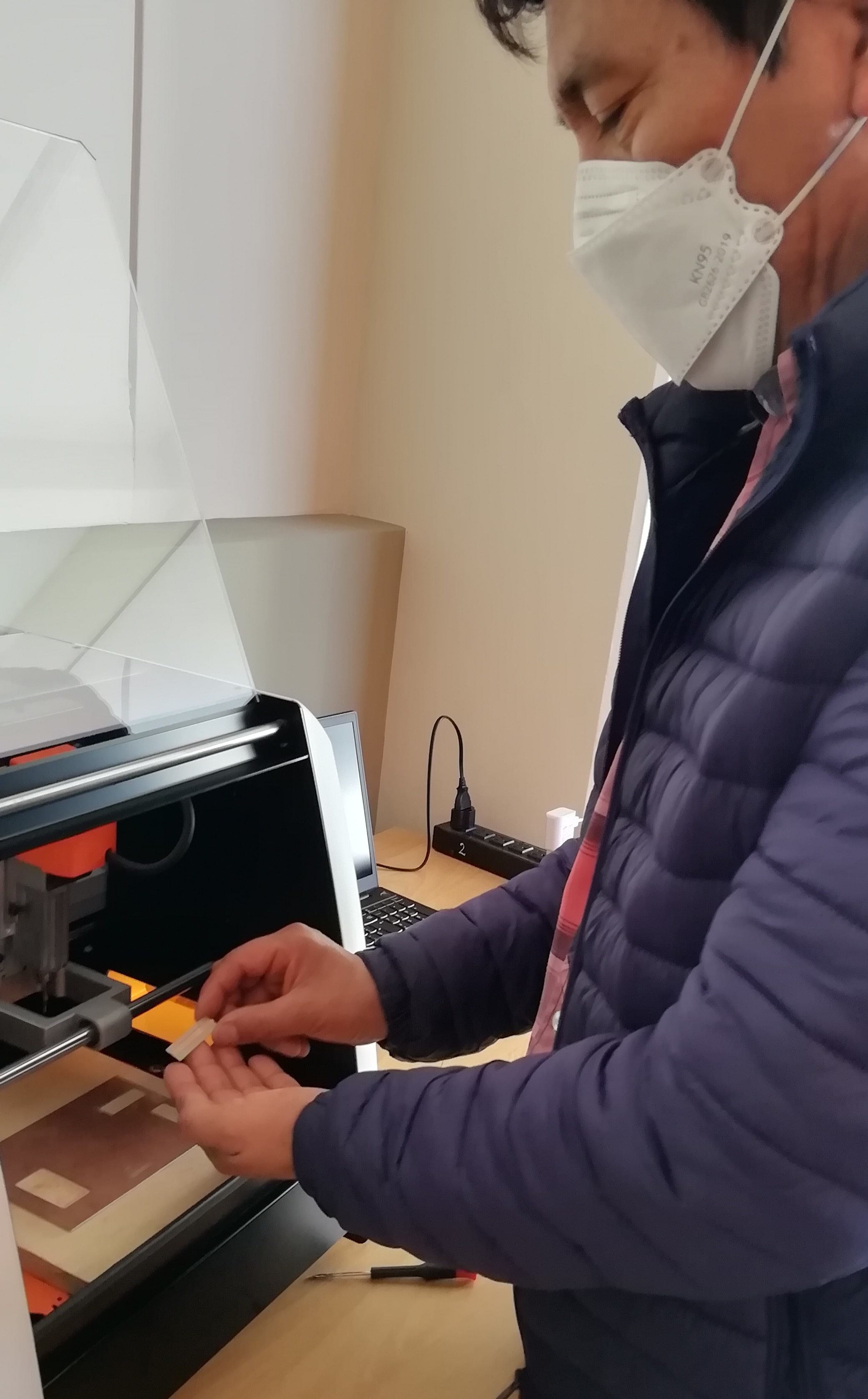
The plate is removed from the slaughter table.
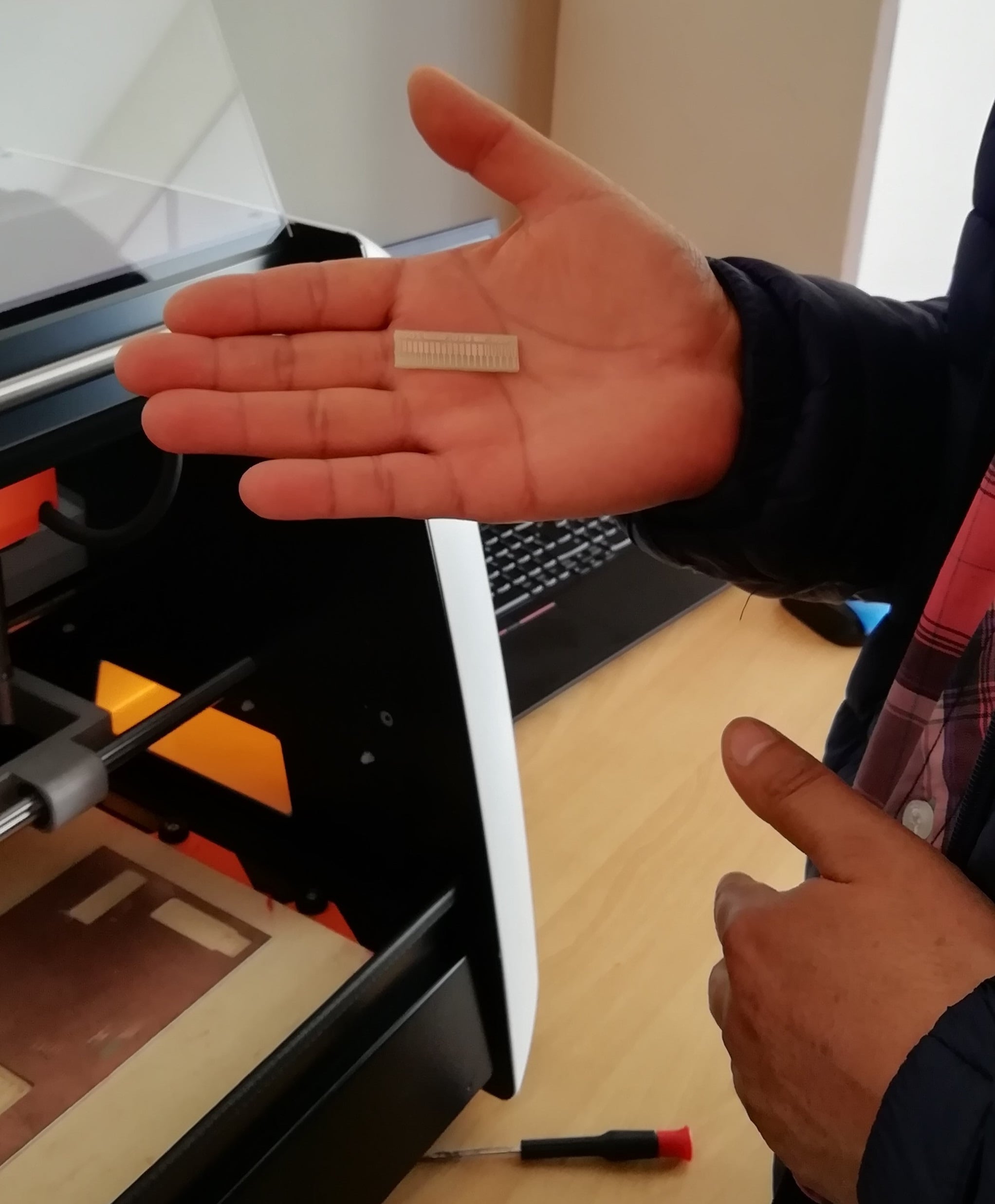
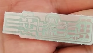
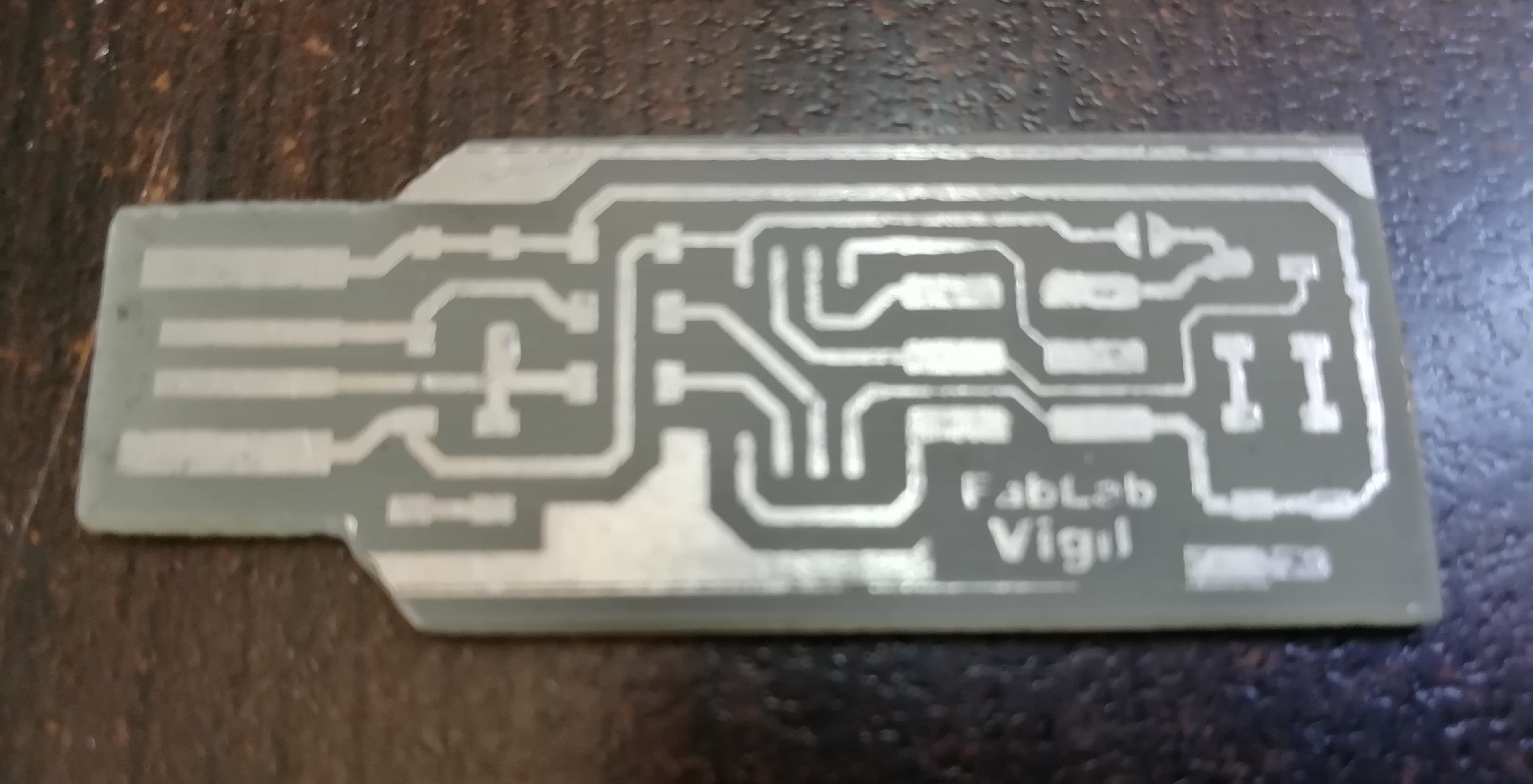
Finally, this is how the PCB looks, ready for its components to be soldered.
Soldering components on the PCB: FabTinyISP
Components
For an efficient soldering of the components on the PCB, the following design scheme was taken as a guide:
Before starting the welding, the welding work table was prepared.
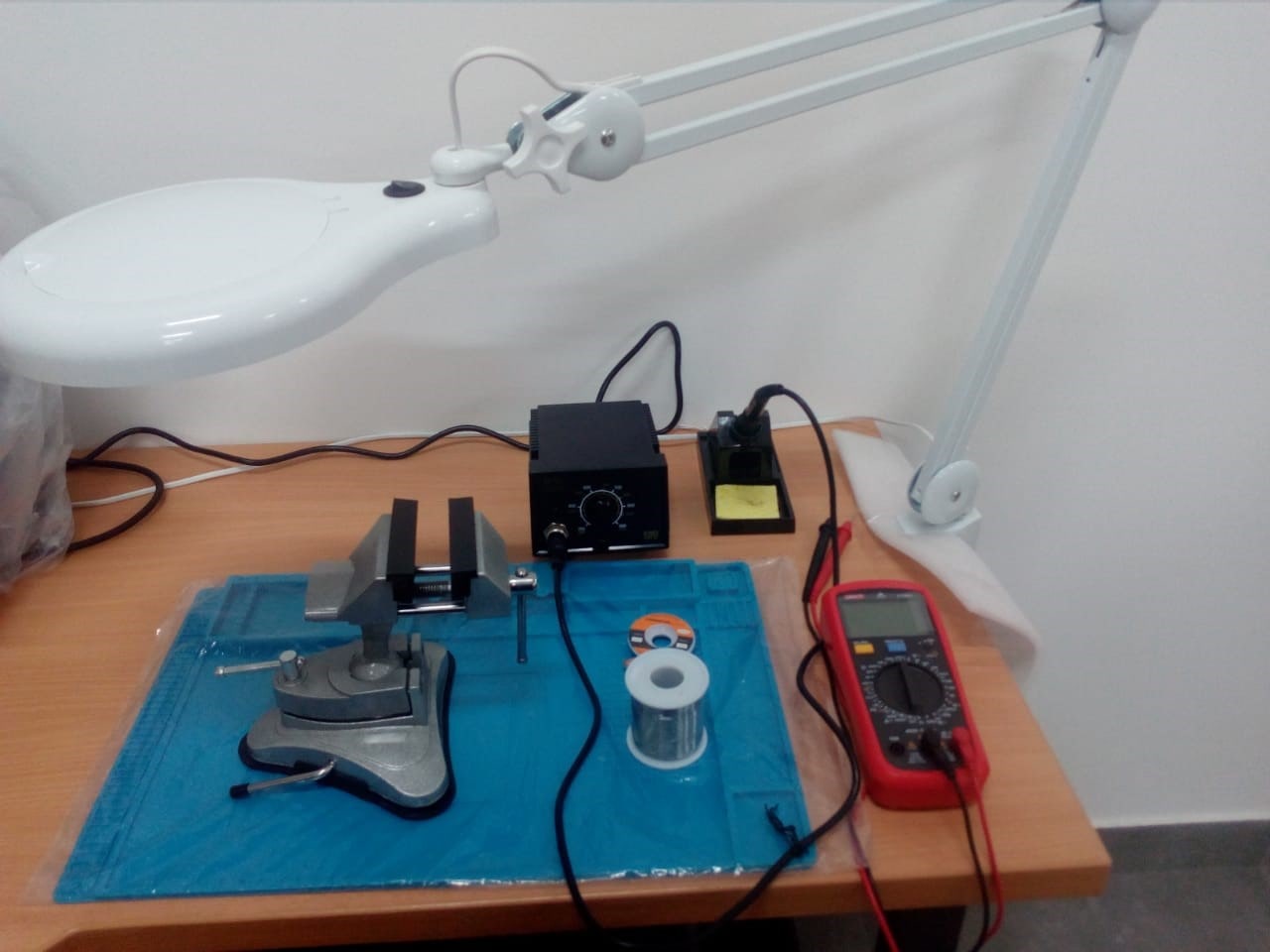
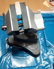
Already in the work area for soldering, to avoid any movement of the board, it was fixed well on an adjustable PCB support.
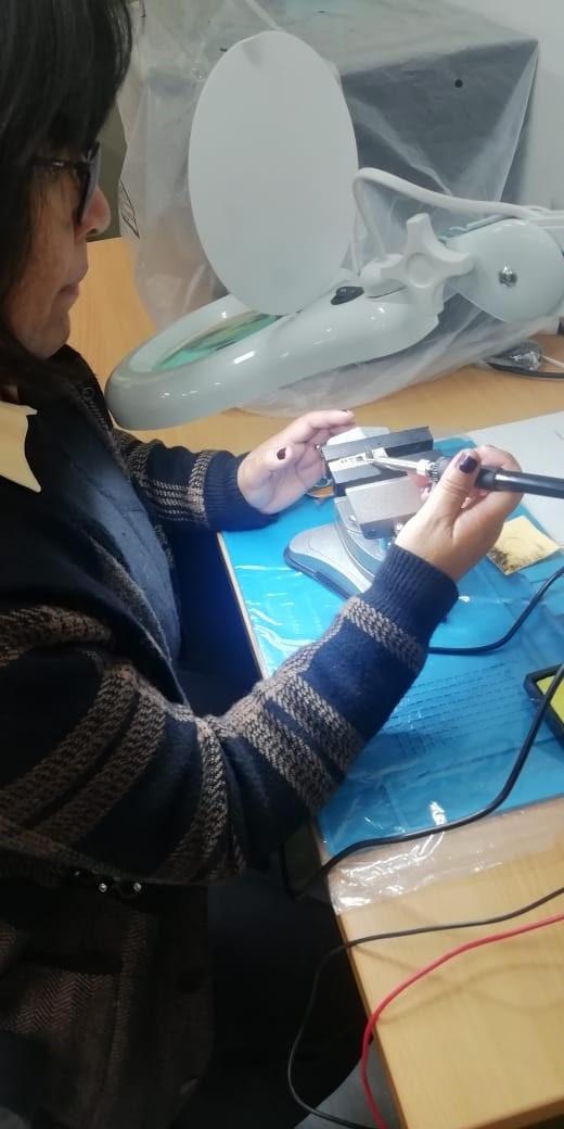
As the components to be soldered are very small, we worked with the help of a soldering magnifying glass.
To start welding (the first time I have done a welding job, of course with the guidance of my colleague).
Finished with the welding, the board was left with a quite acceptable presentation.
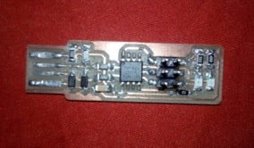
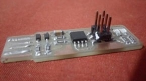
View the plate from another angle.
Doing the respective test with the multitester, indicates that everything is correct.

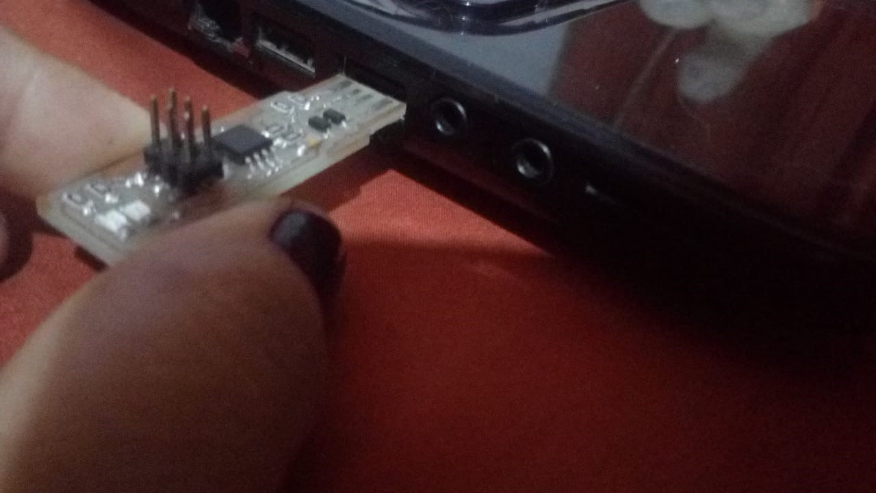
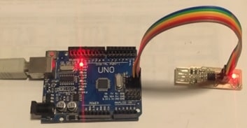
Now connecting it to the USB input of my laptop to verify its operation.
It actually works!!!
Operating software
Following the recommendations of the tutorial, we proceeded to download the file fts_firmware_bdm_v1.zip, and then unzip it.
The Makefile file is selected and opened in Notepad in order to make changes, specifying the name of the programmer and the communication port, thus making the Arduino work as an AVR programmer.
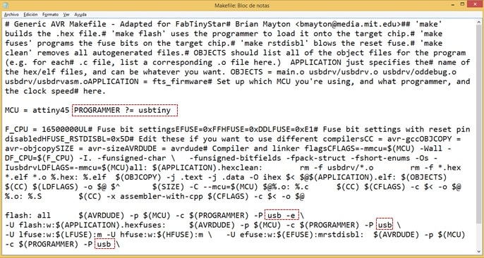
I proceed to make the corresponding changes: for the ATTINY45 microcontroller model, the programmer must be STK500V1 and as for the communication port where the Arduino is connected, according to my case, it must be COM14, at a speed of 19200 bps.
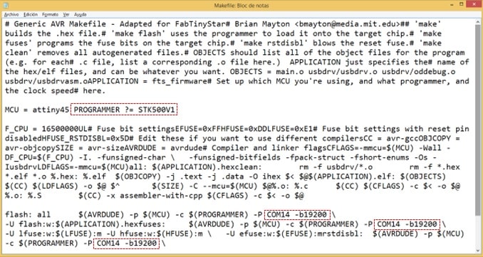
Once the changes were made, we proceeded to save.
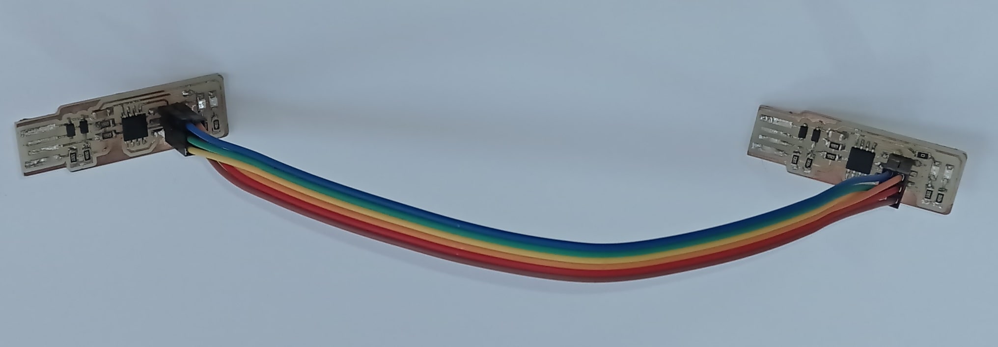
To check the effectiveness of what has been worked, the Arduino is connected to the FabISP using jumper cables.
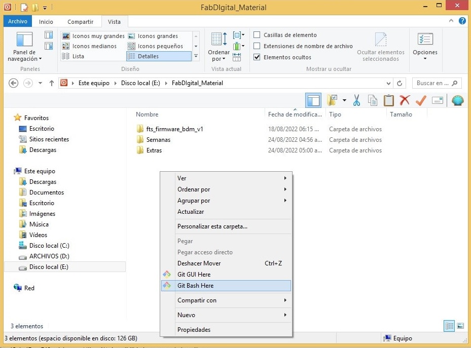
Now proceed to open the fts_firmware_bdm_v1 folder with Git Bash Here.
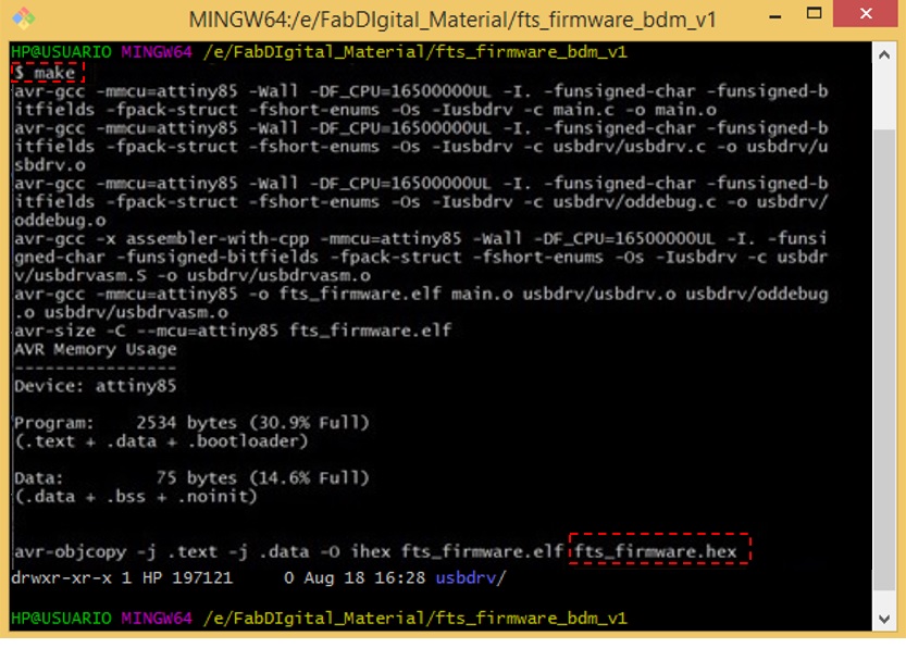
In the command line, the MAKE command will be executed to create the hexadecimal file fts_firmware.hex
Finding myself in Git, I write the following commands to program the ISP using Arduino:
make flash: uses the programmer to load it onto the target chip
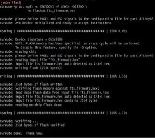
make rstdisbl: blows the reset fuse.
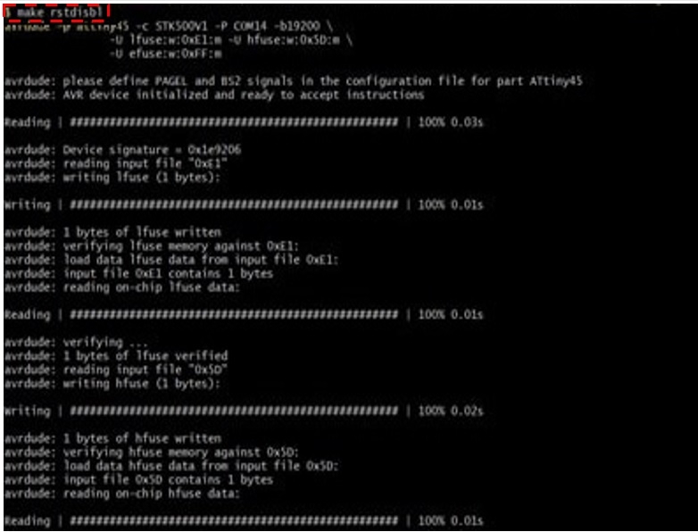
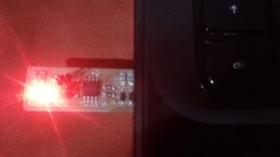
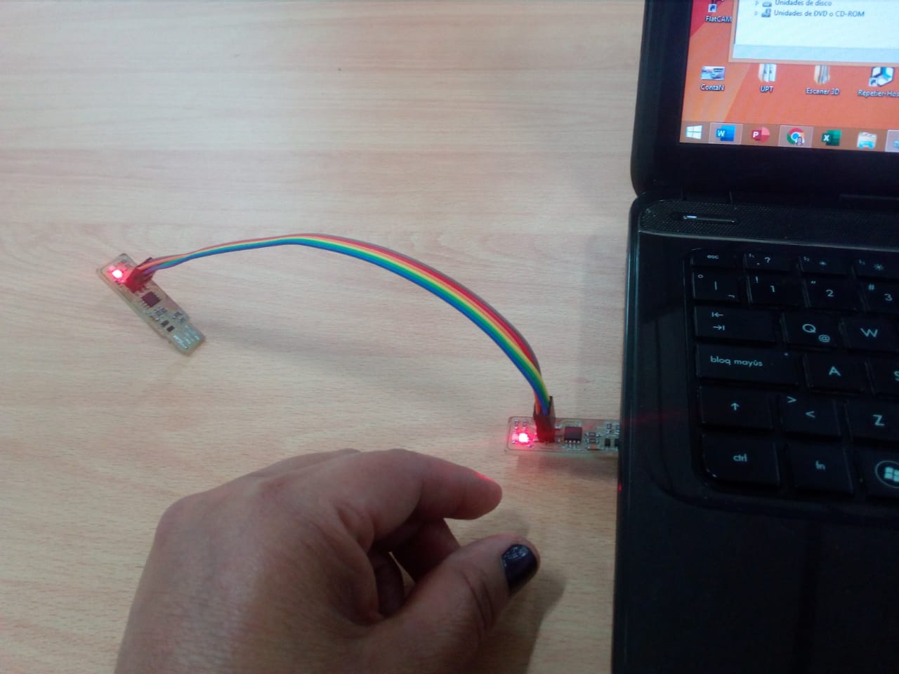
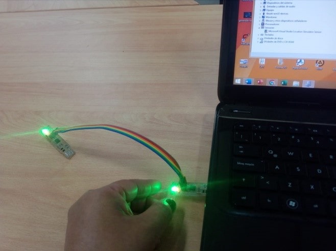
It will be possible to observe that the LED blinks, exchanging the green and red colors, thus verifying a partial programming of the ISP.
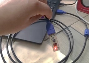
Keeping the FabISP connected to the laptop, proceed to verify the recognition of the ISP controller. For this the Device Manager is opened and the recognition will be checked.
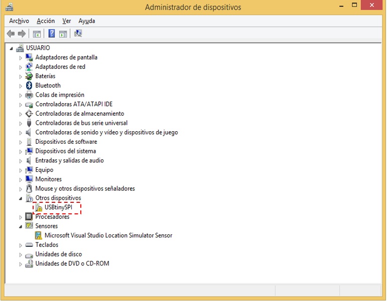
As you can see the ISP is not recognized, so I will work with the Zadig software to install the respective driver.
Making sure FABISP is connected to my laptop, I run Zadig.
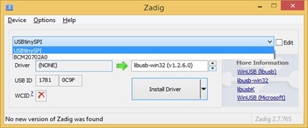
From the dropdown list I select the USBtinySPI device and then I click on Install Driver.
I again check for the existence of the SPI driver in Device Manager.
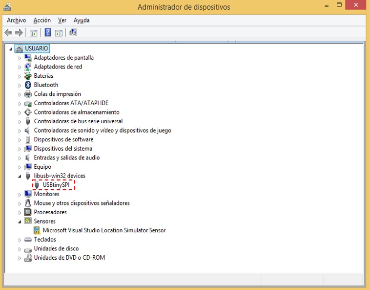
It can be seen that the controller is already being recognized, thus evidencing that the FabISP has been programmed correctly.
So far, it has been possible to build the first FabISP programming board based on Arduino.
Programming a new ISP with the programmed ISP
The FabISP must be connected to the USB of the laptop.
The Arduino IDE should be opened, I see the blinking LED example. Address for pin PB2 of ATtiny 45.
//ATtiny45 PB2 (pin 7) blink

void setup() {
  pinMode(2, OUTPUT);
}

void loop() {
  digitalWrite(2, LOW);   // Turn the LED on
  delay(200);             // Wait for a second
  digitalWrite(2, HIGH);  // Turn the LED off by making the voltage HIGH
  delay(200);             // Wait for two seconds
}
FabISP View
Transferring to ISP for programming
Showing the final product.
Additional
Before the equipment arrived at the Laboratory, a PCB was made using the plate serigraphy process. This is how it looks:
This is a top view of the PCB by the silkscreen method.
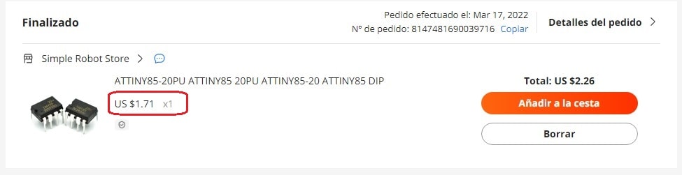
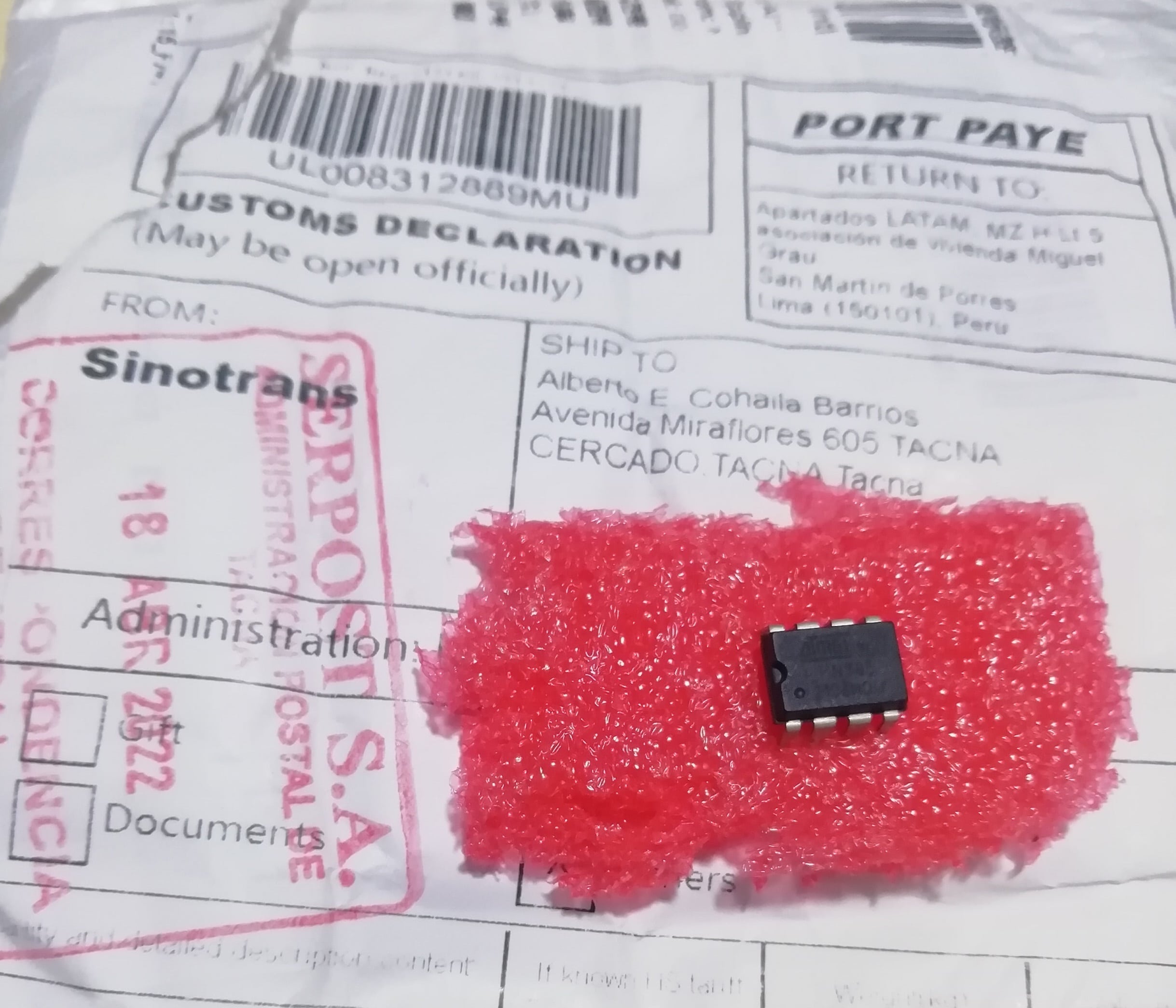
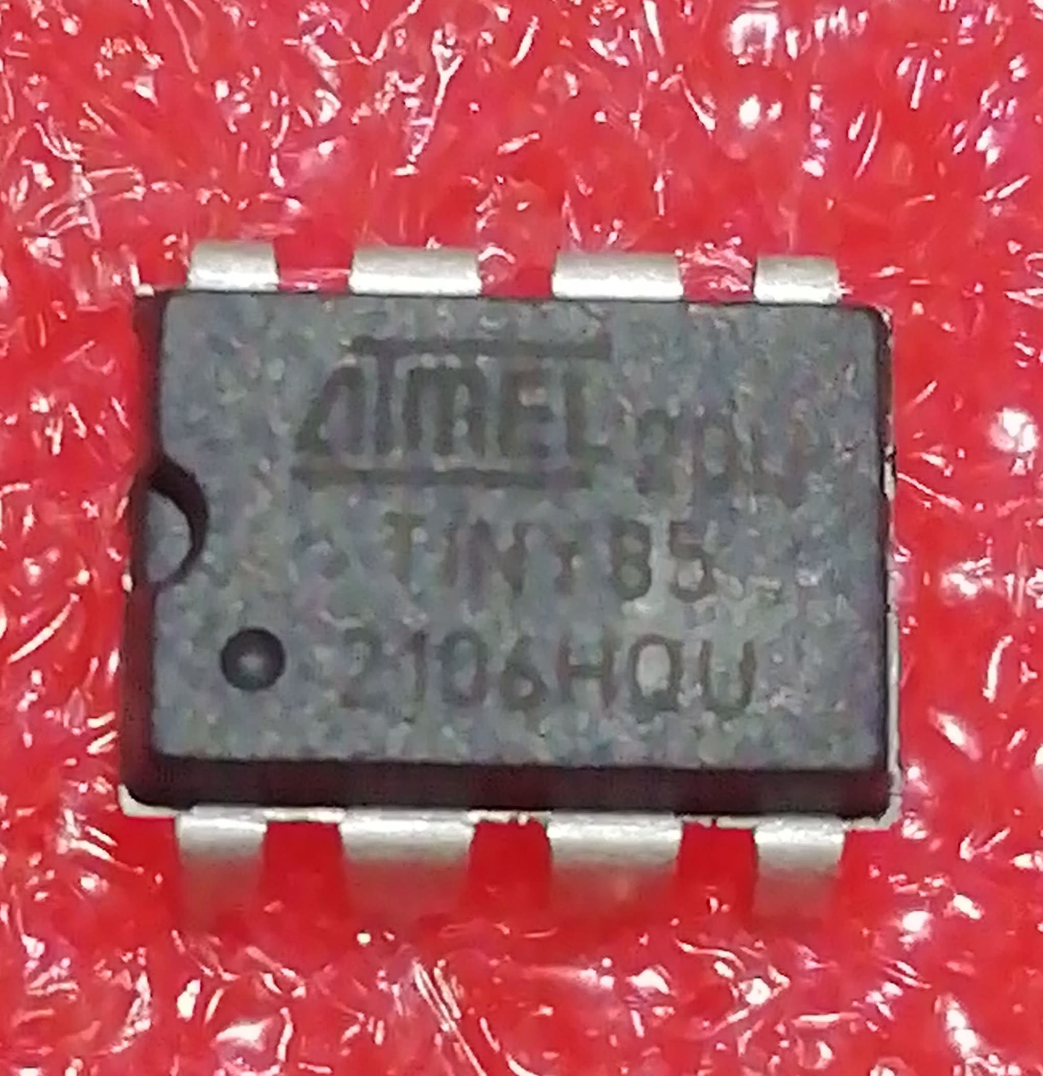
We also ordered 1 ATtiny85 (DIP mount) through Aliexpress, which arrived after 31 days, on April 18, 2022.
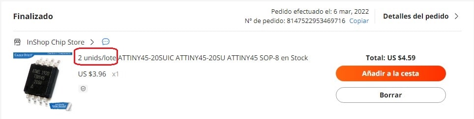
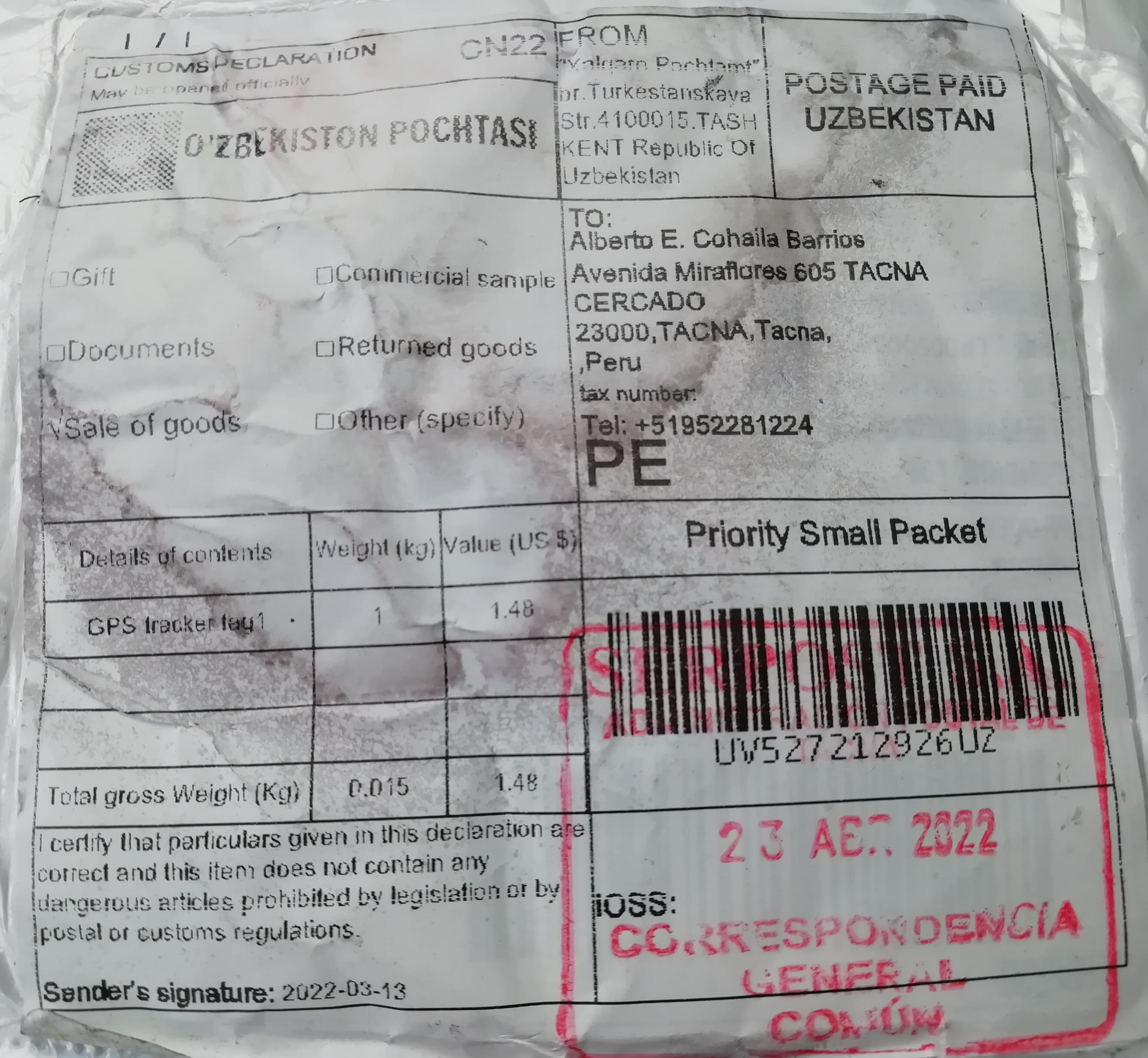
We also ordered 2 ATtiny45 (SOP mount) through Aliexpress, which arrived after 47 days, on April 23, 2022.
Both arrived on April 18 and 23 respectively.
Natives files
| Ord | Description | Files |
|---|---|---|
| 1 | Pattern Test1 | Pattern_Test.png |
| 2 | Pattern Test2 | linetest.interior.png |
| 3 | Pattern Test3 | Rastros.png |
| 4 | Pattern Test4 | Contorno.png |
| 5 | Command files | fts_firmware_bdm_v1.zip |
| 6 | Trajectory file1 | Rastros.png.rml |
| 7 | Trajectory file2 | Contorno.png.rml |