10. Ouput devices
Group assignment
- measure the power consumption of an output device
Documenttion at: Fablab Taipei
Individual assignment
- add an output device to a microcontroller board you’ve designed, and program it to do something
This week I worked on redefining my final project, and wanted to test LED array & speaker as my output device.
Charlieplexing LED array
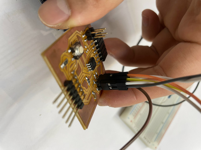
With my Interactive Chinese checkers idea, I need to vontrol lots of LEDs.
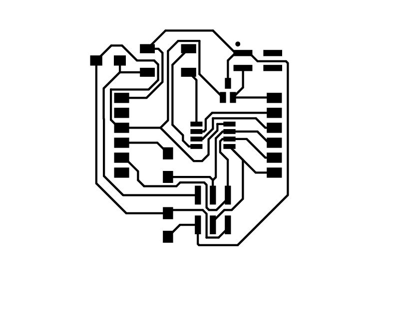
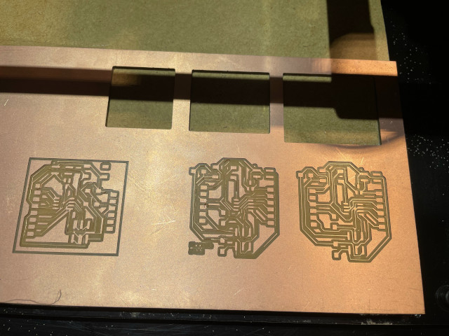
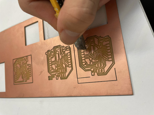
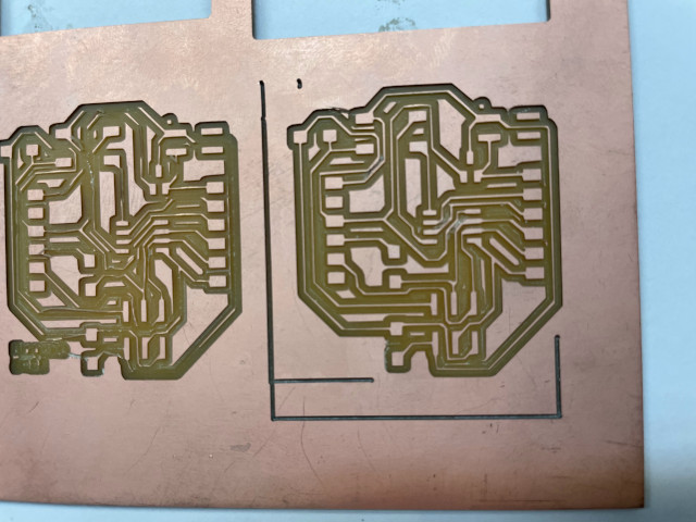
first I wanted to test charlieplexing booard in Output device page. To reduce 0 ohm resistors, I chose the 2 layers board and tried a new way to create it reagrd to Professor Neil said in class.
But later found out there are only “top” and “Bottom” traces files attached, so I combine these 2 images together with Photoshop and milled traces with it.
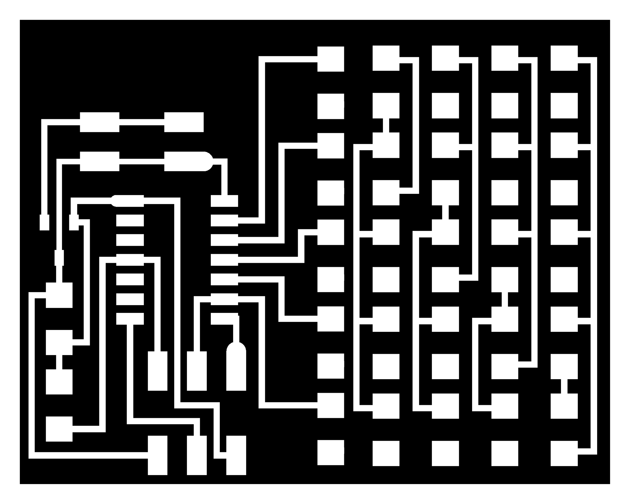
Welcome to use this file but be aware that you need to resize it before milling. The actual size (length x width) should equal to “interior” file below. I tried to resize it when export from Photoshop, but the resolution might decrease. Can use calculation to figure the relationship of PPI, Pixel, inch(mm) calculator.

Next I cut vinyl as a vias layer, but later found it melt when I tried to solder on it. I found some thick paper board and laser cut it instead of vinyl and works.
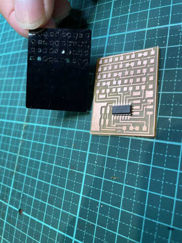
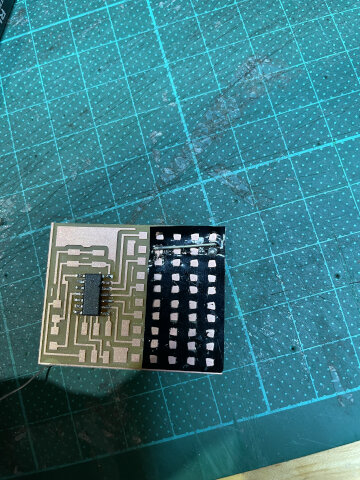
Because the thickness of the paper I used, better put more solder tin on each point, and then cover the paper on it.
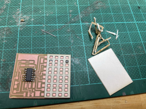
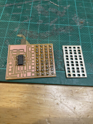
Also instead of using copper tape, I got some solid conductors and rip them, than use the part inside as the top layer.
It’s not easy to solder wires and LEDs together, it took a lot of time. I did wires first and then LEDs, maybe reverse will be easier.
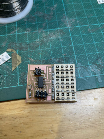
Well the biggest obstacle we encountered this week is the lack of some important parts. Such as “5V regulators” (almost every board needs it), and we ordered already just need to wait.
But for LED array board I don’t see the need for more than 5V power regard to board design, So I just solder a bridge from Vin to Vout. And then when programming it there’s no LED lights up, weird?
I checked with multimeter and from pins to LED the current kept changing so the program is there.
Problems might be:
- The resistor value is to high: No, even changed to 100 ohm LEDs still not light up.
- Bootloader/makefile: Since Attiny44a can only read program through ISP, I thought we can skip the process of burning bootloader. But I found the makefile shows F_CPU = 800000 instead of F_CPU = 2000000. It turns out even set Arduuino IDE clock to “internal 8 MHz” doesn’t work.

Well, it turns out that was me not connecting wires, and while I reconnect resistors and LEDs, it works! but something strange is one pin of attiny44 didn’t output any voltage so 1 row and 1 column not blinking.
While trying to understand how to burn bootloader correctly, I learned 2 things.
- Attiny44 doesn’t need to burn bootloader first.
- Makefile is used to create the program, and since we had the program from Professor Neil, it’s not necessarily to use. (Learned some concept from article in Chinese)
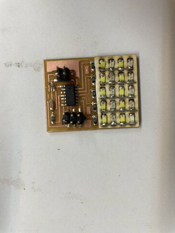
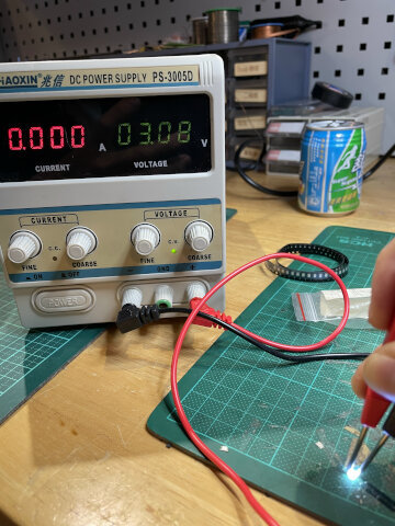
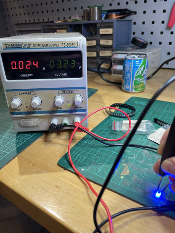
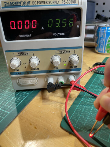
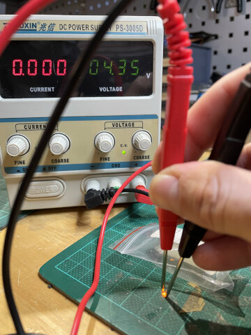
LED voltage testing (with different colors)
I found white, yellow, blue and red LEDs in lab, and test their voltage versus brightness.
It turns out white and blue require lower voltage and they are brighter while increase voltage; Red and yellow require more voltage and darker in comparison.
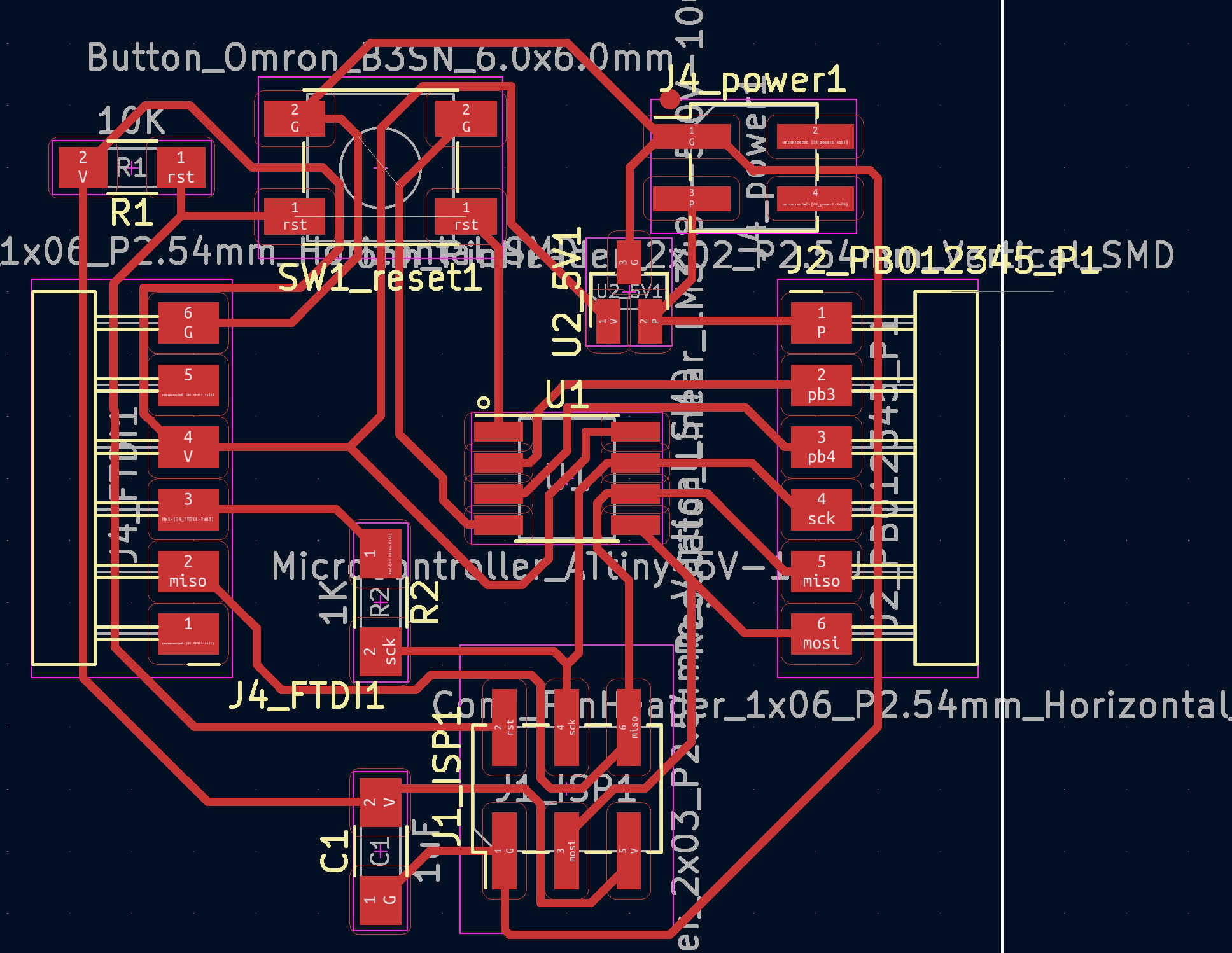
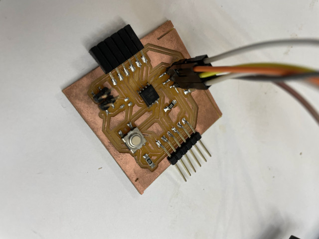
Board design: Attiny45 core module
Update: latest board version see week 14
I started from creating a attiny45 board which should be reusable in the following week, thus I check all example boards of attiny45 and design the common part (core module).
while it’s also my first time to use KiCad and it’s quite different from EasyEDA. Learned a lot from this video. And also found some useful tips from experience.
- Hotkeys: L for lable (copy-paste to do many times for one lable); W for wider trace (up to your pre-defined width); E for edit trace.
- Do the “file -> board setup” before routing.
- Check “constraints”: minimum clearance (your endmill parameter)
- Check Pre-defineed sizes: set width will become the default sixe when you create new traces. And you can also choose which pre-define class you want to use on top left when routing.
- Check net classes: I added a new class with different width, and able to change exsisted trace’s width. (select trace, select all tracks in net, Press E, check “use net class width”) Update: try to edit the “Default” setting for clearance & trace width you want, or have to change each of them after routing and find many errors.
- Run Elertonical rule check in schemetic before open PCB tool, run DRC (design rules checker) in PCB editor before export it.
- If you want to edit schemetic design while routing PCB, always run “footprint assignment tool” in schemtic first and run “update PCB with changes made to schemetic”.
- While routing, “shove mode” is an intersting way to try, other traces can be responsive while you are editing the current one.
- After routing, another way to change width is to press “W” after choosing existing trace after routing, and it should become wider reference. But be aware is there is different width trace in your selection, they will get wider together (stay different). Thhis may refer to the setting also on top left
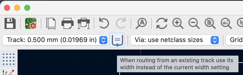
I tried many times, even 0.33 mm trace and 0.4 clearance failed a bit, need to use utility knife to clear and it’s super hard.
Use 0.5mm trace and 0.4mm clearance should be fine! And do give power source a wider trace.
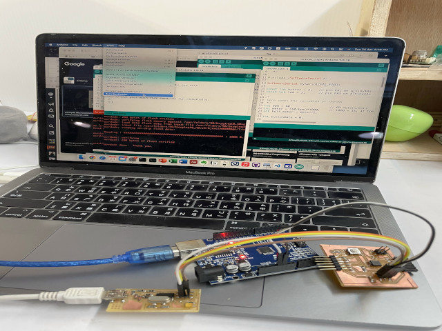
The way to burn bootloader is choosing the target board infomation (Attiny45/internal 8 mhz) and choose Programmer (USBtinyISP) in Arduino IDE.
The result is that board still doesn’t work well and copper trace even detached from wood part after days…
Update: Tips for SVG to PNG in Adobe illustrator (Ai) is using: go to File -> Export -> Export As. And choose “others” while setting resolution to 1000. Also be sure to check the “Use artboards” option. reference
Notes for using reflow: hot air gun is a powerful tool, set air control smaller or it will melt lots of stuff including the green cutting pad, or make it too long to detach or burn copper. Don’t use it for eletronics part easy to melt such as pin header…(Use it for 2*3 pin header with lower air and temperature below 400 is fine, but if pin just stand above solder it may detach later, need to fix with solder gun and get pins cover with solder)
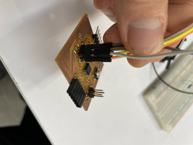
Buzzer testing with attiny45 core module
I started my testing with a buzzer, this kind of buzzer has a built-in driver circuit , so it doen’t need another resistor. Once some current flow through, it will generate “beep” sound. (shown as image below)
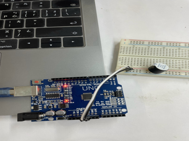
And then I simply connect my core Attiny45 board with bizzer through dupont wires and it works. Later I found a example code and burn it into my board with the following setting, but something weird happened.
Connect setting: Using both FabISP & Arduino Uno. FabISP is used to programming through ISP (6 wires); Arduino UNO is used to provide 5V power because FabISP board cannot supply enough power.
I detached the the USB cable of FabISP and connect buzzer with GND and PB1 pin on my board, but only heard a stable “beep” or many slight “beep” sound. If using PB0 or PB2 instead of PB1, I can hear a slight melody! Somehow PB1 is defined as output in code…
After some debugging, I tried out a way that if I keep the USB cable of FabISP connecting, PB1 output is fine.
Later with Yoyo’s help, we found out maybe FabISP is the problem. If it connect with my board through ISP (6 wires) and leave its USB cable unplug, the microcontroller on it shut down and allow some signal from my board come and go. This may leads to some interruptions on my board; On the other hand, While USB cable of FabISP is conenected, the microcontroller wake up, and there’s no interruption.
Lesson learned: after programming the board, get rid of any unnecessary wire connect to it (especially when they connect to another board).