Basically week 2 in our collection of subjects that dive deeper and deeper into the electronics side. In week 4 I learned how to mill and solder a PCB. This week we went one step farther back along the full design process and learned how to design the outline and traces of a PCB and some basics about the main components found on boards, such as resistors and capacitors.
Assignments
Our tasks for this week are:
- Group assignment: Use the test equipment in your lab to observe the operation of a microcontroller circuit board
- Individual project:
- Redraw an echo hello-world board
- Add (at least) a button and LED (with current-limiting resistor)
- Check the design rules, make it, and test it
- Extra credit: simulate its operation
Hero Shots
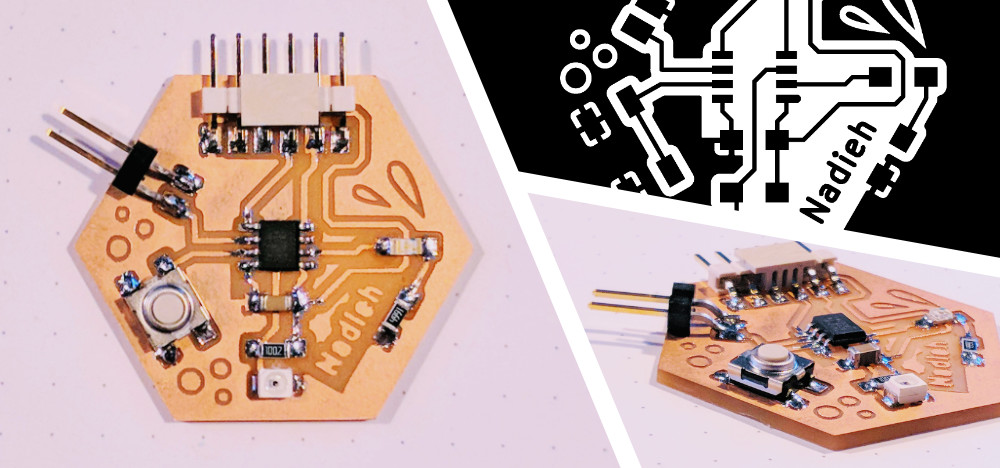
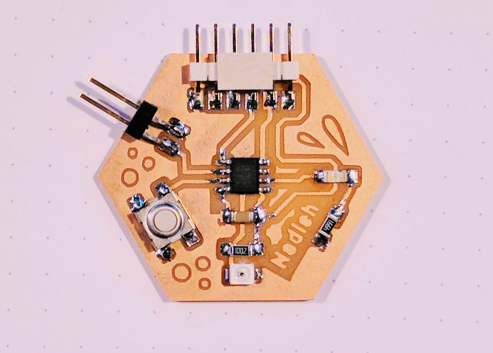
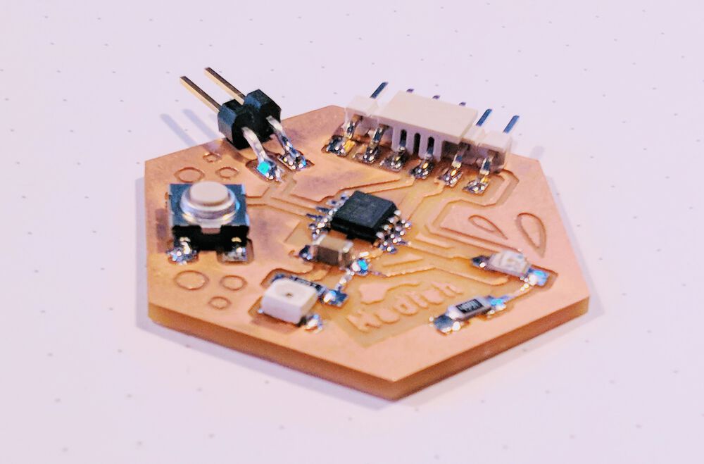
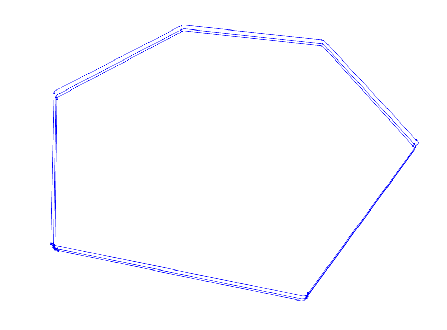
Showing my final hexagonal-hello-world-PCB for the tl;dr and hopefully showing you why the rest of this very long blog could be interesting to read (⌐■_■)

Electronics Components
This week we’re learning the basics of an electronic circuit, which is a closed loop composed of electronic components such as resistors, capacitors, microcontrollers, through which an electric current can flow. These components have to be connected to each other with some sort of conductive material, such as conducting wires or copper traces.
The basic units within an electrical circuit are:
- The voltage | measured is volts | written as V | It is the difference in electric potential between two points. Batteries are common sources of voltage in many electrical circuits.
- The current | measured in amperes | written as I | This is the stream of electrons moving through the circuit.
- The power | measured in watts | written as P | This gives the electrical energy that is transferred through the circuit (per unit of time, with watt being the amount of joule per second).
The relationship between these three elements is P = V * I. There are some interesting mathematical relationships between voltage, current, power and resistance depending on whether the circuit is connected in parallel or series. I won’t go into that here, but this Wikipedia page explains more about it.
Another important basic measure of circuits is the resistance which I’ll explain soon.
Circuit
For a circuit to be “functional” you need at least one component to be a source of power, such as a battery. The simplest circuit is a battery + resistor. You need the resistor, otherwise the battery would short circuit; all the electrons would move from one end of the battery to the other in “one swoop” having drained the battery. You basically need an obstacle in the circuit to have the electrons move with control (all circuit symbols and diagrams in this section made with Circuit-Diagram.org).

A general note, for the Fab Academy we’re working with SMD (surface mount device) components as opposed to THT (through-hole technology), and using the 1206 standard in terms of the size, which is about as small as it can get while humans can still solder it with their hands.
Battery
To have an active circuit where the components are performing tasks, a power source is needed. This can be a battery, such as the 9V block, the 1.5 AAA or 3V coin batteries, but it can also come through a USB connection with a laptop for example.
Batteries deliver a voltage difference between their + and - poles. The plus side is often called VCC, V, V+, or +V, while the minus side is called GND for ground in circuit diagrams. The symbol for a physical battery looks like a (series of) long and short dash, as you can see in the image above. When the power source is more abstract (such as on PCBs with USB power), the plus side is often denoted with an arrow, while the ground can be a single dash.

Power can come in AC (alternating current), but is generally always transformed into DC (direct current) when it’s used inside a machine. The alternating current is really only used to transport the power without losing too much along the way. We’ll therefore always assume a DC power source is used.
The AC that comes into our homes has a really high value of around 230V in the Netherlands, this is again to reduce the energy lost in transport. Transformers will transform that down to the typical 5V, 9V or 12V used by many machines.
Resistor
Resistors, as the name suggest, create a resistance of the electrical flow. They have two end points and have no specific orientation (they are non-polar). Resistors behave according to Ohm’s law which states that the resistance is the voltage divided by the current: R = V / I. Using the formula for power we can also write the equation for power as P = V * I = R * I^2
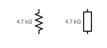
The symbol for resistors is sadly not completely uniform. The official IEC (International Electrotechnical Commission) symbol is a long rectangle, but in the US they stick to a zig-zag line.
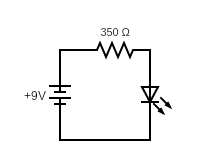
One very common usage of a resistor is to control the current flowing through a component of the circuit. For example, if you have a 9V battery and an LED that can handle 30mA max, you need to place a resistor together with the LED with a resistance of at least R = V / I = 9 / 0.03 = 300Ω. Without the resistor the current would get much higher than the 30mA because the LED creates practically no resistance. Using resistors we can control the current in various parts of a circuit by adding resistance. It converts energy into heat.
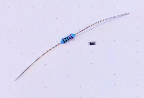
The resistors that we use are generally created using thin film; using metal, metal-oxide or carbon film. Their values range from 1Ω to around 10MΩ in what we’ll come across at the Academy. There are also special 0Ω resistors, but these function as bridges across traces on a PCB.
For THT resistors colored rings are used that convey the Ω value, while for a SMD resistor, the Ω value is printed on the front:
Every resistor has a maximum power rating. To not overheat your resistor, the power running across it should kept under that maximum rating. For safety, it’s best to choose a resistor that can dissipate twice the power. Generally, the bigger the resistor, the higher the power rating.
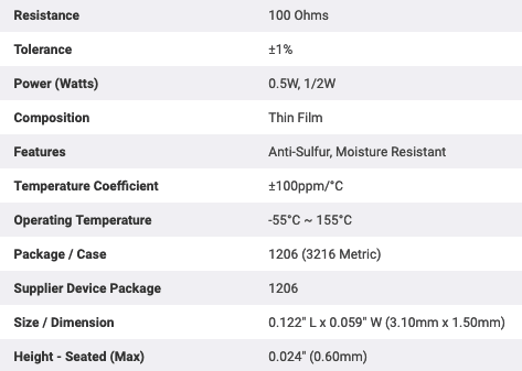
You can read off all the specs of a resistor from its datasheet or product attributes, such as this 100Ω example.
I found that this video explains the basics of resistors really well (also explaining why resistors generally have such odd values).
Capacitors
Capacitors store electrical charge, somewhat like a battery, although it’s stored in a different way. Generally, it can’t store quite as much energy as a battery, however it can charge and release its energy much faster. Capacitors stay charged for a (little) while even after the power source is cut off.
The unit value of a capacitor, its capacitance, is measured in farad, given by the symbol F. The values used on our boards are generally really small, around micro, nano, and pico values. The schematic symbol of a normal capacitor is two parallel lines, which is inspired by the actual way a capacitor works (we won’t go into the other types, such as polarized):

Because they act like a “tank to store current”, they can be used to smooth out noise in the power supply (such as when converting from AC to DC power). It basically helps to keep a constant voltage throughout the circuit.

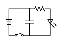
For example, say we have a circuit with an LED and a switch that turns on and off really quickly (mimicking “noise” in the power), the LED will be blinking. However, if we connect a capacitor parallel to the LED, as you can see in the diagram below, the LED will receive the stored energy from the capacitor when the switch is turned off. The LED will thus stay on for just a little while longer, and if the energy stored in the capacitor is enough to bridge the time between the moment that the switch is turned on again (thus recharging the capacitor again as well), the LED will seem as if it’s emitting light constantly.
A capacitor can also be used to quickly supply power in case a component wants it. If I understand correctly, power supplies can be “slow” to react to, say, a microcontroller that suddenly asks for more power, causing the voltage to drop until the power supply truly responds to correct the drop/ask. For this decoupling capacitors are used. They are basically a “fast” charge storage near the microcontroller. So when the microcontroller turns on, it will (first) draw from the capacitor which is really fast in responding, giving the power supply more time to react.
Some other uses that I could find have to do with timing, because the charging and discharging rates of capacitors can be accurately calculated. And also with frequency blocking I believe, but I did not investigate this further.
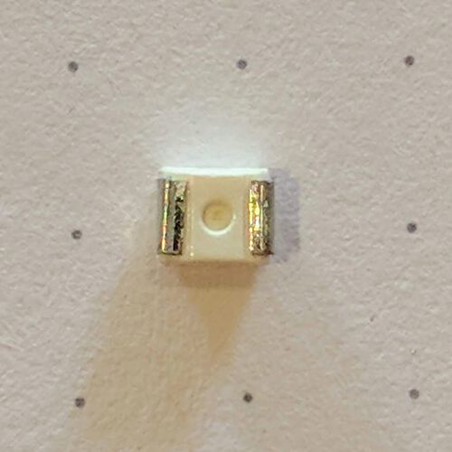
SMD capacitors are tiny rectangles with a color that signifies its capacitance value, while for THT capacitors you can have several difference kinds of shapes, such as cylinders and flattened spheres, with the values written on top.
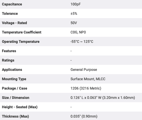
Capacitors are rated to handle a certain maximum voltage. When the voltage is higher it will explode. You can find these values in the datasheet, but I believe that for the SMD capacitors that we use, this voltage is so high that we’ll never reach it. For example, for this 100pF example the voltage is at 50V, much higher than the ±max 12V that will probably ever run across a board.
This video was really good at explaining capacitors, using some very good metaphors with water and water tanks.
LEDs and Diodes
LED stands for light-emitting diode. It’s a specific kind of diode, but one that’s become more “famous” than the “normal” diode. An LED emits light when current flows through it. However, a diode is a component which allows the current to only flow in one direction.
A diode has an anode (positive) side and a cathode (negative) side, with the current being able to flow from the anode to the cathode side. A diode can thus (functionally) only be installed in one specific direction. Generally, the cathode side of an diode is marked somehow, such as a white line or an arrow mark on the bottom side.
The symbol for a diode is a triangle with a stripe, with the triangle placed to show which way the current can flow. For an LED there are two arrows next to the triangle (to mimic light being emitted).

Only letting current flow in one direction, diodes can be used to protect a circuit from accidentally connecting a power source in the wrong direction, and to help go from AC to DC current. But LEDs can of course be used simply to have a (blinking) light.
As I mentioned before, an LED is non-ohmic meaning that it creates no resistance in the circuit. Connecting a battery straight to an LED will create a short and blow up the LED. You need at least a resistor.
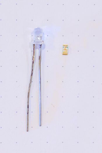
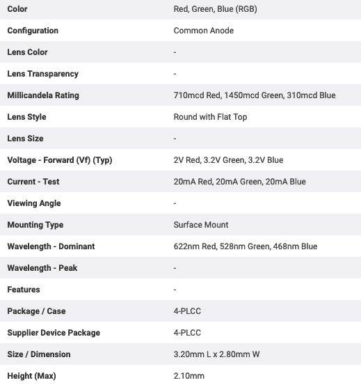
However, there is something called a voltage drop, forward bias, or forward voltage (Vf). Diodes need to have a certain threshold of voltage running through it, before any current will flow across it. There is also a forward current (If) which is the maximum current it can handle. You can generally find these values in the datasheets or product attributes, such as for this RGB LED example that has a Vf of 2V - 3.2V (depending on the color) and a If of 20mA.
To calculate the resistor value that you need to protect your LED the formula is basically Ohm’s law but with the difference between the voltage of the power supply and the voltage drop of the LED: R = (V_power - Vf)/If. For the LED example from above, let’s use the 2V Vf of the Red color, and take a 9V battery, then we need a resistor of (9 - 2)/0.02 = 350Ω. In case you don’t want to do the math yourself, you can also use ledcalculator.net
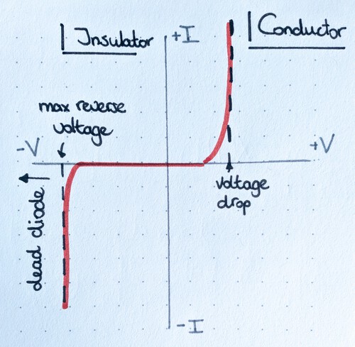
There is also a maximum reverse voltage. If you were to apply a voltage that is higher than that to a diode in its reverse direction, the diode can no longer stop it, breaking the diode, letting the current flow, and probably destroying the whole circuit as well. I drew the small chart below to convey the concepts of the voltage drop and maximum reverse voltage (with the minus sign meaning “reverse” voltage and current):
Besides LEDs we could also come across Zener diodes, which allow you to clamp a voltage (say you want the voltage to not get higher than a certain value).
To learn exactly how a diode works, check out this great video, such as why there is a voltage drop.
Microcontrollers
A microcontroller is basically a small computer. They are examples of integrated circuits, meaning that all the components are hidden inside. They are designed to perform a predefined task (you give input, the controller gives an output) that you program it to do. It has no working memory so you can’t store anything on it, and there’s no operating system on it.
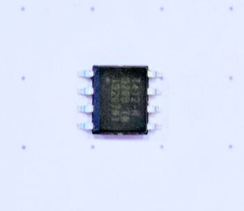
During this week we’ll be working with the ATtiny 412.
Since it’s a complex component, you can’t capture its properties in a simple table. Instead a datasheet can be found for each microcontroller on the website of each manufacturer. For the 412 this contains 594 pages! On page 13 we can see the block diagram that shows all of the components within the ATtiny 412:

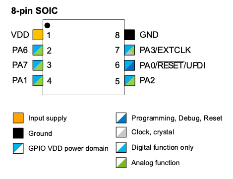
Whereas on page 14 there is a diagram that reveals what functions the different legs of the microcontroller (can) have, and a marker to assess the chips physical orientation (the black dot in the upper left):
Other Components
I won’t be able to give an exhaustive list of electrical components that can be placed within a circuit, but here are a few more that I came across this week.
Transistors
Transistors (from transfer and resistor) are used to amplify or switch electronic signals and power. They allow you to control the amount of current going through, from all of to none of it.
There are different types of transistors. The most common one are the BJTs (Bipolar Junction Transistors). However, I believe that during the Fab Academy we’ll be working with MOSFETs (Metal-Oxide Semiconductor Field Effect Transistors) only, specifically n-type enhancement MOSFETs.
A transistor has three legs, for a MOSFET the middle leg is called the gate (G), while one of the outer legs is a source (S), and the other is the drain (D).
For these n-type MOSFETs, when a voltage is applied between the gate and the source, then current is allowed to flow between the drain and the source. Even more so, they are variable resistors controlled by voltage. Depending on the voltage applied between the gate and source, the resistance between the drain and source will vary. A low voltage will mean a high resistance, and vice versa.
I won’t go into more details, but this video explains some of the important parameters, such as the V_GS (threshold voltage), V_DS (drain-to-source voltage), R_DS (drain-to-source resistance).
Phototransistors
Phototransistors are a type of transistor that are able to sense light levels and alter the current according to the level of light it receives.
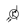
This video explains how the workings of a phototransistor can be seen as a reversed LED on which light is shined, together with a transistor.
Resonators
Resonators are used as clocks inside a circuit. They are a critical part of a microcontroller. They have a piezoelectric material inside, such as a quartz crystal, that resonates at a certain frequency when a current is passed through. The symbol for the crystal is basically a capacitor with a rectangle inside (although they are also often drawn with two capacitors attached to it, creating a three-terminal IC).

For the old ATtiny44 chips the internal clock wasn’t accurate enough and thus an external resonator was needed. However, for the newer ATtiny412 this is no longer needed.
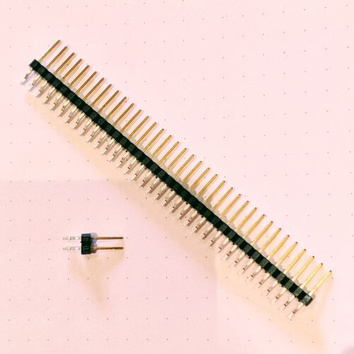
Pin Headers
These are a form of connectors to be able to connect electronic boards and other components to each other.
Buttons
A button or a switch let’s you make a connection when you press it. This can be used to turn on an LED while the button is pressed for example.
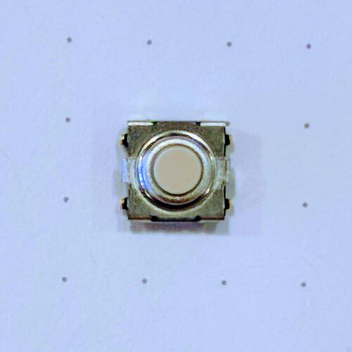

Internally, each side of a button is connected. Therefore, you can’t place a button in any of the four different positions on the four pads. However, a button doesn’t have a polarity, so out of the four possible ways to place a button, two are correct. As long as you place the button with its connected sides along the pads that will be connected.
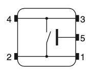
I looked up the datasheet of the button from the image above, a B3SN-3112P which shows a tiny schematic of the switch mechanism within.
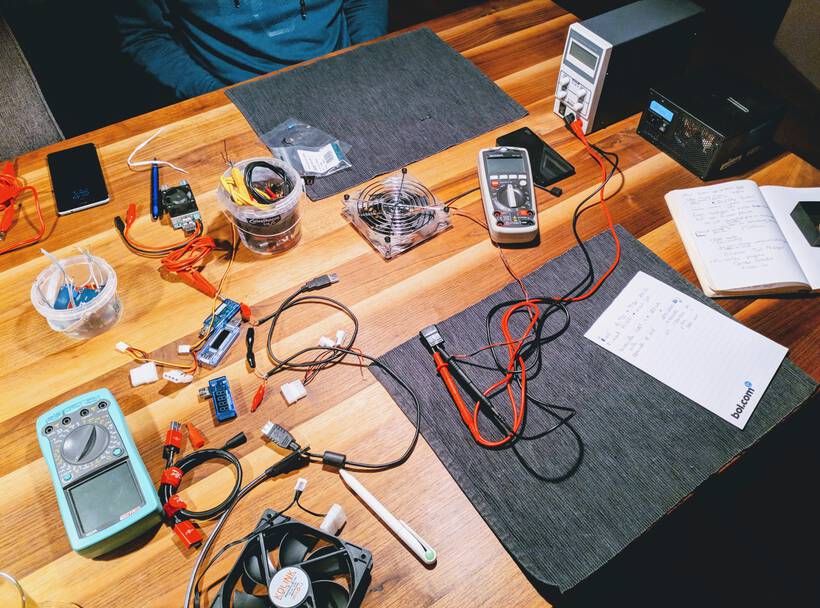
Measuring Electronics
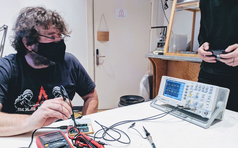
To understand and debug our boards, we need to be able to measure them. To learn more about this we were introduced to, and played with, several types of machines during our group assignment; the multimeter, an oscilloscope and a logic analyzer.
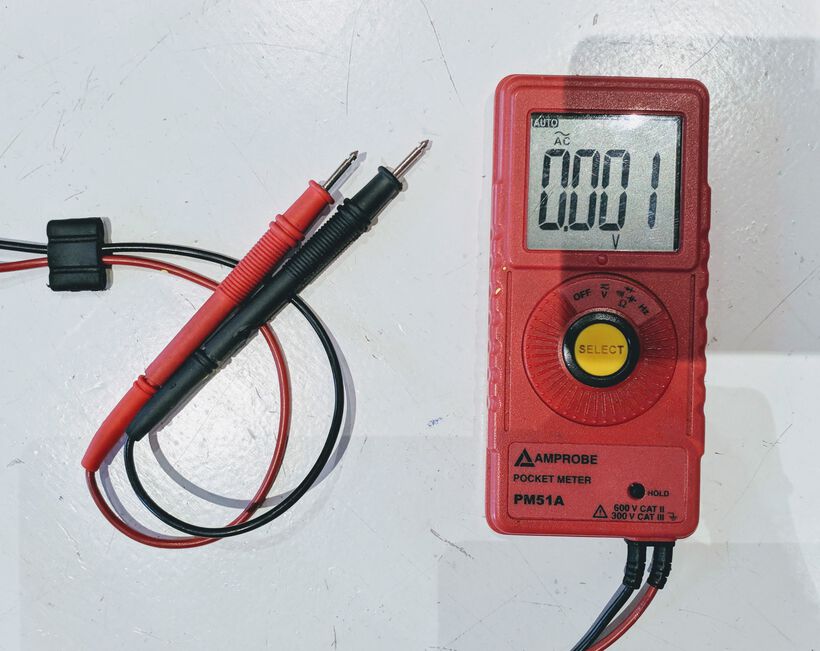
Multimeter
As the name implies, a multimeter can measure multiple things. The number of different options depend on the exact model. For the multimeters that I played with I’ve measured: voltage (both AC and DC), the resistance, the current, the voltage drop across a diode, and a continuity tester.
A multimeter has two wires coming from it, a red one that is positive and a black one that is the ground. With these you make connections with the component or system that you want to measure, always trying to connect the ground first.
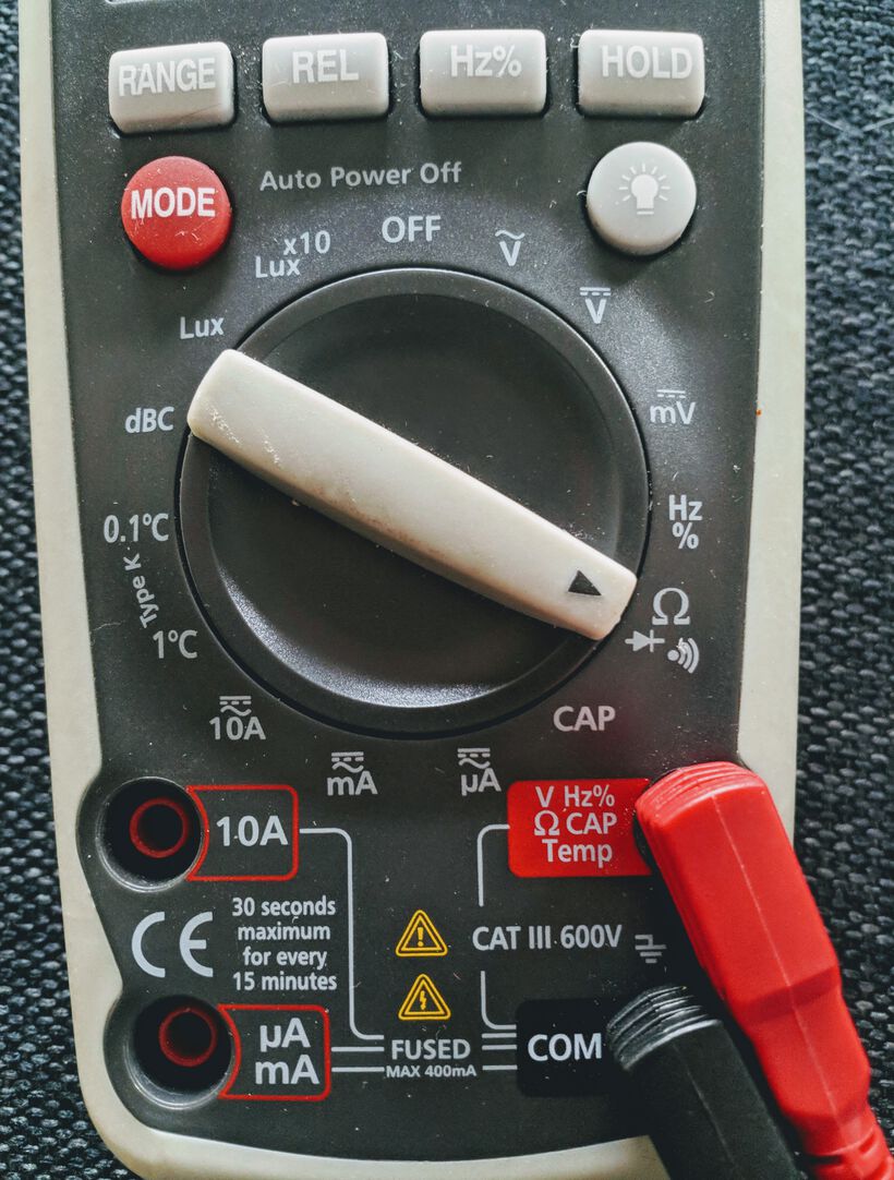
With a more advanced multimeter that can also measure the current, you often have 4 holes along the bottom to plug the red and black wires into. The black (ground) wire will always be in the same hole. Depending on what you’re measuring the red one needs to be in a specific hole, otherwise you might damage the meter. Generally two holes are for measuring the current, with one for a high current (10A in the image above right), while the other is for a small current (around mA and μA in the image above). To measure any other unit that requires the cables, you use the final hole (the red wire is plugged into this hole in the image above).
You turn the multimeter on and choose the right mode, generally by rotating a central dial to point towards the variable you want to measure.
To measure the voltage from a power source you choose the V sign. You can measure AC with the V sign that has a sine wave above it, or DC where the V has a stripe and three dashes above it.
At home I plugged the red and black wire into a power socket with the AC voltage mode on (after asking my partner of it was really ok to do so for the 10th time), and got a reading back of 230V. That’s probably all I’ll be doing with AC voltage measuring.
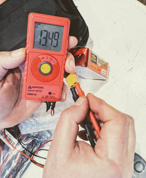
Switching to measuring DC voltage, in the lab we measured the voltage of a giant battery pack of 18.5V, which still gave 13.5V:
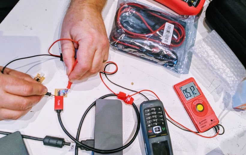
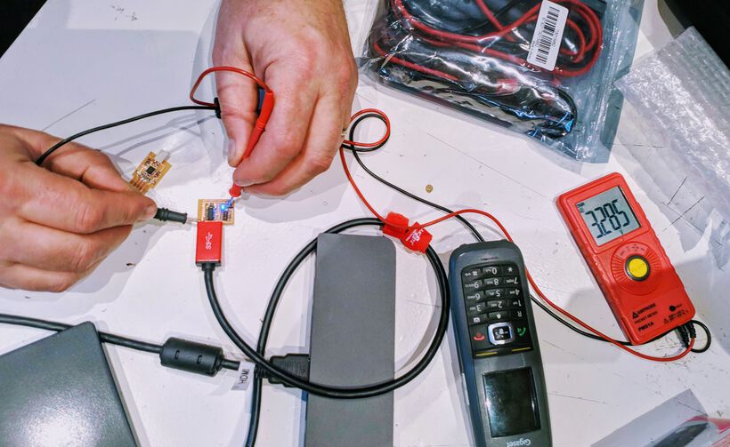
A JTAG board was also tested while plugged into a USB port. Before the transistor the voltage read as 5.12V, while after the (3.3V) voltage regulator it read as 3.285V.
It’s also quite common to measure resistance. Rotate the dial to the combination of the Ω, diode sign and sound icon (which looks like a wifi symbol). These three all have to do with resistance, but are slightly different. You have to press some button to switch between them (it differs per meter, on the red one it’s the yellow central button, on our multimeter at home it’s the red “mode” button).
Putting it on Ω will let you measure the resistance. Simply hold the two ends of the rods against the two end of a resistor, wait a few seconds and you’ll get the resistance.

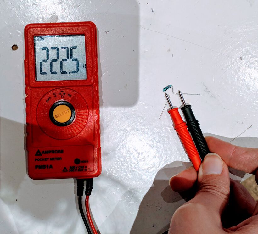
Resistors that are already soldered onto a board are rather hard to measure. I think it’s because they’re part of a circuit, it could be that you’re measuring a loop/line not through the resistor, but through a different section? I’m guessing that perhaps the larger the resistor value (and if another loop exists) the bigger the chance that you’ll be measuring something else. I never asked this, but at least my two experiments on a UPDI did support this theory; I measured only 3.7Ω across a resistor that was labelled as 4.99kΩ, while I measured 53Ω across a resistor that was marked as 49Ω.
At the same setting, but a different mode (the sound icon) you can measure continuity. I’ve already talked about this in week 4 when I was measuring the traces of my UPDI and JTAG boards. In this mode the multimeter will make a sound when a loop is created between the red and black rods (just hold them against each other to test). You hold one rod to a point on your board, and the other rod at a different place, and if those tw points are somehow connected via traces and components the multimeter will make a sound. You generally use this to check you soldering; that no connections have been made that shouldn’t be there, and that you haven’t lost any traces or connections either.
Finally, with the diode icon you measure the voltage drop across a diode.
Those are the values we measured while in the lab, although at home I also experimented with measuring the current with our own multimeter.
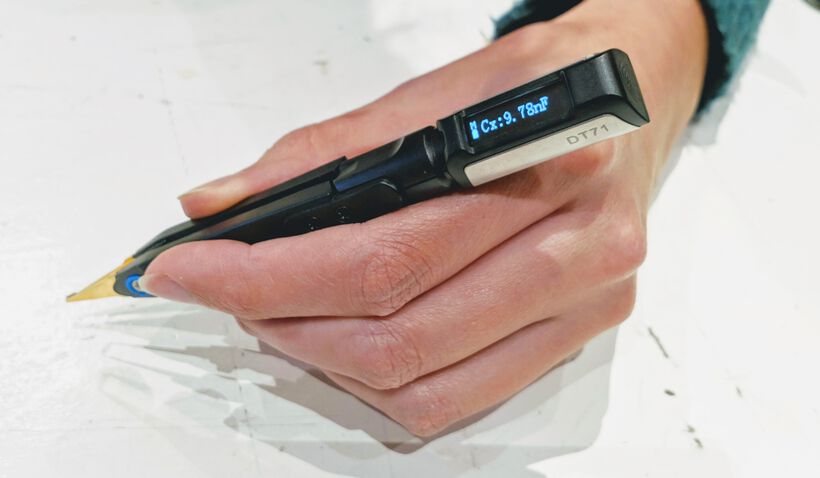
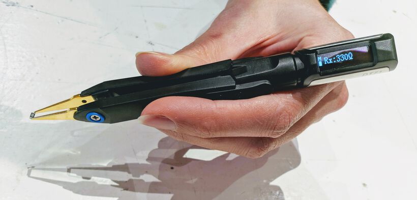
Digital Tweezers
This was a really nifty multimeter-like tool at the lab. The DT71 Mini Digital Tweezers by Miniware are tweezers that can measure a whole array of values. It even figures out exactly what you’re trying to measure; resistance for resistors and capacitance for capacitors.

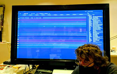
Oscilloscope
Nearing the end of the day Henk turned on the oscilloscope. A machine that makes me think we’ve gone back in time at least half a century, solely based on the fact of how the screen looks (*^▽^*)ゞ
Although you can measure many things with a multimeter, it only shows you an average value across time. With an oscilloscope you can dive deeper into this and see the signal across a time window, the waves going through a circuit, which is very handy in case you have a changing voltage.
For example, you might be seeing an LED that seems to be “on” at all time, but the oscilloscope can reveal that it is indeed blinking, but apparently faster than the “refresh rate” of our eyes.
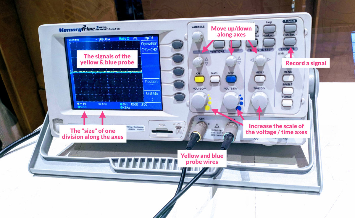
This oscilloscope has two probes with which you can measure a signal, a yellow and a blue probe, thus you can measure two signals at the same time.
On the graph time runs along the x-axis and voltage across the y-axis. With the two buttons right above the point where the probe wires connect to the machine you can set the voltage scale that is displayed on the y-axis, while the dial to the right of the blue button lets you adjust the size of the time window displayed along the x-axis.
The values below the graph in the window give the voltage and time of one division along the chart (the distance between a set of dotted lines).
With the smaller dials a little above the bigger dials you can move along up/down along the axes for the voltage and back/forth for the time.
With the Run/Stop button you can start a recording of a signal (and stop it again with a second push). Afterwards you can inspect the signal with the buttons that I just explained. This can really help for changing signals where things go to fast, or happen only once (e.g. a button press) and you’d really like to dive into what happened.
Henk touched the yellow probe to a circuit and showed how the signal can change through the press of a button on the device. There was always some fiddling with the dials to make the signal visible within the chosen time frame and voltage scale:
He then made a blinking LED from which we could read the square-wave pattern (typical for digital devices) of when it was on and off.
And although interesting, Henk mentioned that he doesn’t often use an oscilloscope to debug his devices, preferring to use other means, such as a logic analyzer.
This video explains how to understand the signal that you see on the screen and what the most commonly used buttons on an oscilloscope do, very handy.
Logic Analyzer
The last measuring device we got to see was a USB logic analyzer, which is similar to an oscilloscope in that you can see the digital waveform/signal across time, but you analyze it digitally. Furthermore, a logic analyzer can only see if something is at a low or high voltage, above or below a threshold, not any details in between, so it’s not a precise as an oscilloscope. It’s like a sniffer, you eavesdrop on the pins of a microcontroller and can see the bits being passed.

The output from a logic analyzer needs to be viewed on a computer. There are several software program’s available, such as Logic2 from Saleae, and PulseView, which is open-source.
By choosing which communication protocol is being used along the port that you’ve monitored, you can decode the bits that were captured.

We didn’t get into this part a lot so I can’t really give more information. But from what I saw Henk doing it seemed very interesting, so I ordered my own logic analyzer that weekend. Hopefully I’ll learn how to actually use it in the future.
Home Schooling
That evening my partner pulled out basically every electronic measuring and power device he had, together with some interesting machines to measure and I got an extended lesson at home (*≧▽≦)
Apart from the variables I’d measured in the lab I also got to measure current. It was also fun to interact with devices that can change the voltage, and see the effect on how the machine functions (e.g. a fan rotating slower and faster) and how it affects the current.
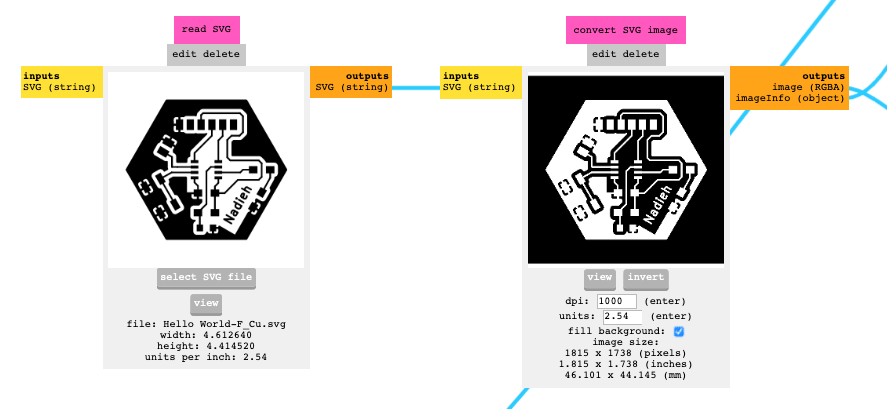
Making a Hello World Board
For our individual assignment this week we need to (re)create a “Hello World” board, based on the ATtiny412 blink board, but also add a button, LED and phototransistor to it. Our instructor Henk gave us the schematic to recreate that contained all the components needed and which parts needed to be connected to each other.
KiCad
The main program to design our board with is KiCad and open-source electronics design automation suite. It’s a collection of several different programs that work together to help in the design of a PCB.
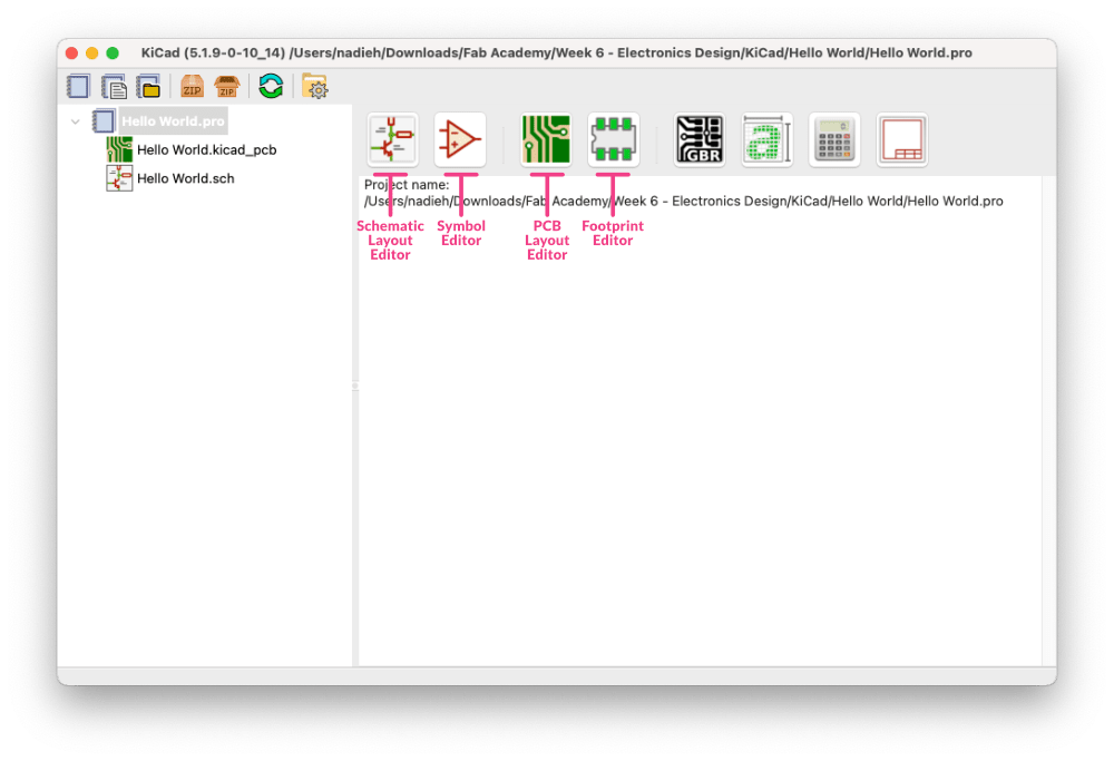
With KiCad opened, click the Create New Project in the top left. I called my project “Hello World”.
Libraries
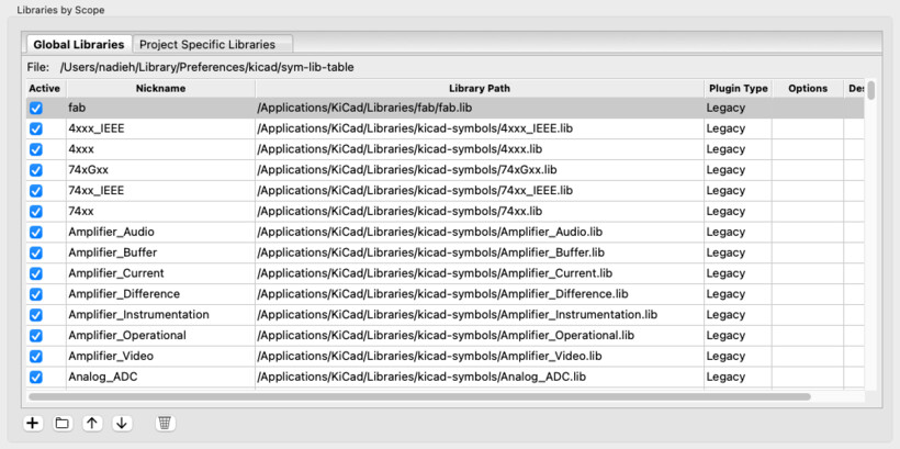
To make it a lot easier to design my board, I had to add several symbol and footprint libraries to it. Specifically the Fab Electronics Library for KiCad that contains the symbols and footprints of (almost) all the parts that we’ll be using during the Academy.
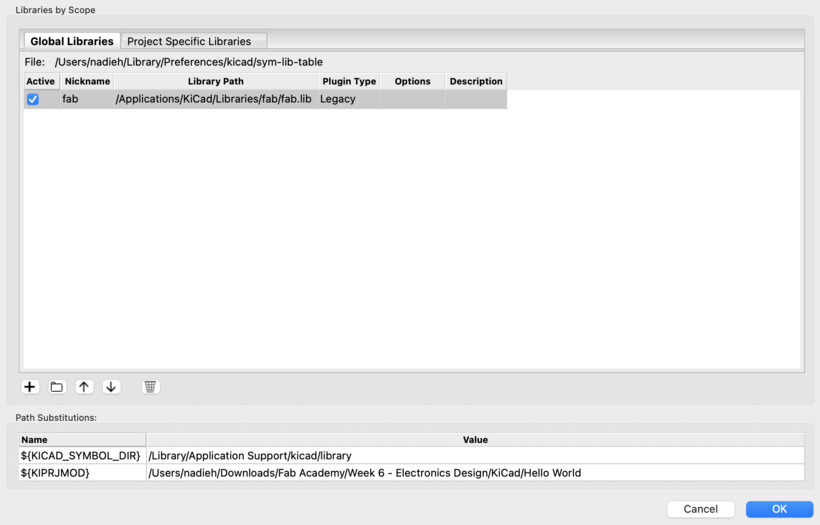
I downloaded the .zip file and followed the steps as outlined in the Installation section of the library’s page. I created a Libraries folder in the Applications/KiCad folder and put the fab folder in there. In KiCad I then went to Preferences and Manage Symbol Libraries. However, if this is the very first time you’re adding symbols (or footprints), it appears that you first need to configure the library table, since I saw the following pop-up:

Because the “recommended” option was greyed out, the Create an empty global… seemed the most logical next option and I selected that. Next, a new window appears that is the Project Specific Libraries tab. Switch to the Global Libraries tab, and press the little folder icon button along the top. Browse to the place where the fab folder is located, select the fab.lib file and open it. Now the Fab Academy symbol library is added to KiCad.
I repeated the same process for the footprint library, this time going to Manage Footprint Libraries and eventually selecting the fab.pretty file.
Finally, I added the fab academy folder’s location to the path by going to Preferences -> Configure Paths and I added a new path called FAB pointing to the location of where I saved the fab folder:

Even though this should contain basically everything we’d need, during our instruction day, we found out that it doesn’t contain a power source or ground symbol! Therefore, we also need to install the default libraries from KiCad itself.
The process is basically the same, however, the KiCad library contains ±100 separate .lib and .pretty files. After some searching I wasn’t able to find a way to import them all as a single library. However, when you’re in the browser window to add a new library, you can select the first .lib file, scroll down to the last one and SHFT click it, which will select all the files in between as well. Each separate lib file will then become a new row within the Global Libraries window:
And do the same for the footprints. Strangely, enough I didn’t have to create a path variable for these new KiCad libraries to work (which makes me wonder if it was really needed for the FAB library). I also downloaded the 3D models zip that is provided on the KiCad download page. However, it’s 5.6Gb and my laptop is always straining for space, so I haven’t added these to KiCad, because it feels like a nice-to-have.
Many (larger) vendors of electronic components will also have symbol and footprint libraries of the components that they sell, such as those from Digi-Key. That page also contains some really good introduction videos to KiCad. If I ever need to create a new symbol myself, this video in particular explains each step very well.
Schematic Layout Manager
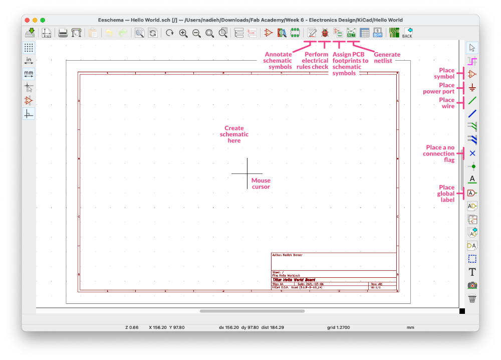
With all the libraries loaded, I went to the Schematic Layout Manager to start designing my board: picking the components I need and connecting them by creating the circuit diagram.
A new window will open with an empty schema. Below I’ve annotated all the buttons that I’ve used to create my final schematic:
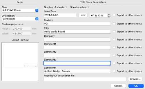
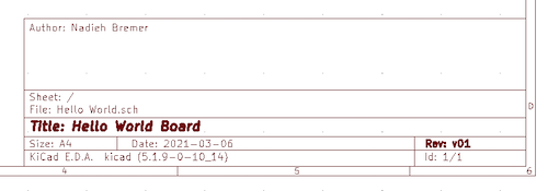
You can add some metadata to this file that will appear in the lower-right section of the schema. Go to File -> Page Settings and fill in whatever you think is relevant (strangely, the comments are placed in the reverse order on the schema):
Which then looks like this on the schema:
Adding All Components
To place parts, click the Place Symbol icon and click anywhere in the schema. This will open up a new Choose Symbol window from which you can select your part, such as a resistor.
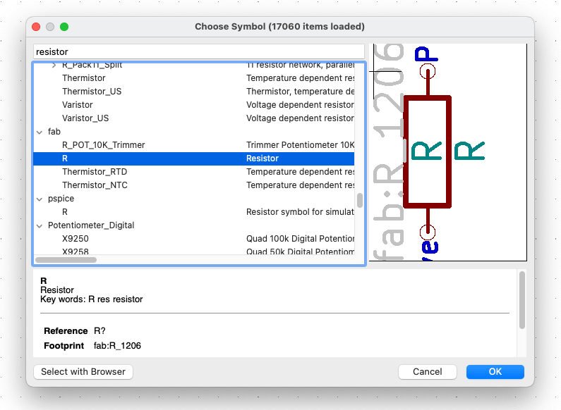
Press OK and click the board at the location where you want to place the symbol. In case you aren’t happy with the location, hover your mouse over the component and press M to move or R to rotate the part.
To place another component press A, which will open the Choose Symbol menu again. However, in case you simply want to add the same component, hover over the one already on the schema and press C to copy it to your mouse and click anywhere to place it.
For some parts it can be handy to add the value to it, such as the resistance of each resistor. For now, the resistor just says R, but this can be changed by right-clicking the part, going to Properties and choosing Edit Value.

In the window that shows up, replace the R by its value, such as 5K.
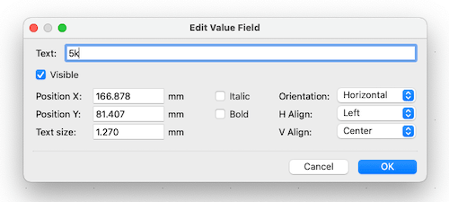
We can also jump straight into the value editing window by pressing V while hovering over the component.
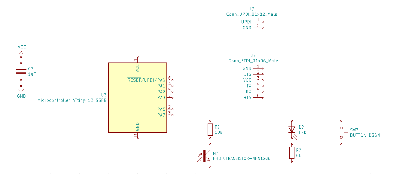
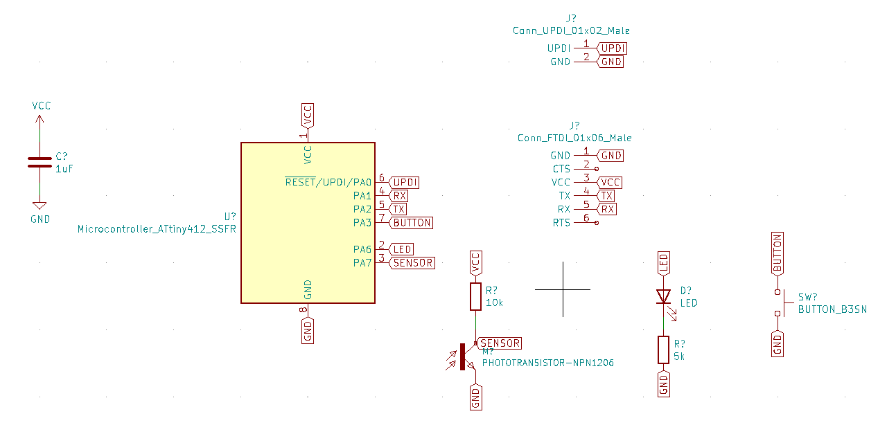
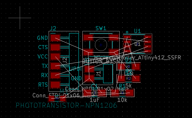
With the schematic that we’d received from Henk I proceeded to place all the separate components, which ended up as follows:
Connecting Components
Next, I have to connect these components. There are two ways of doing this: draw wires between the connected points, or work with net labels. I don’t think there’s a set rule on when to use the one over the other, but I get the sense that you use wires for the most basic connections, such as between an LED and a resistor, but use the labels for connections to pins of a microcontroller, pin header, and the VCC/GND.
To draw wires, select the green Place Wire button along the right (or press SHFT+W). Click at one end-point of a component and click the other end-point that you want to connect it to. You can also hover over one end-point and press W to make a wire start there. To create a 90 degree angle in the wire, click at the point where it should bend.

I’ll label all the other connections. Click the Place global label button from the right and click anywhere in the schema. This will open up a Global Label Properties window. You can change the label name. Note that when you place multiple labels, anything that has the same label, the program assumes that these will all need to be connected to each other (in the next steps). You can also make some changes to the orientation, size, style and shape of the label in this window.
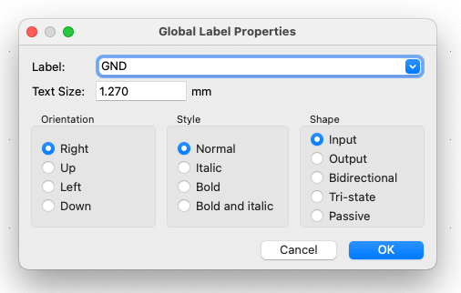
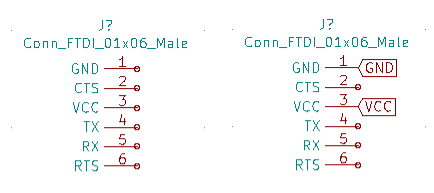
Press OK to and then click your mouse at the location where you’d like to place the label. If you forgot or didn’t orient the label correctly, you can still press R to rotate the label before placing it. With the label placed, the small circle of that pin will have disappeared. See for example the difference of having placed two labels to the FTDI connector:
If you’ve misplaced a label (I switched the TX and RX labels on the microcontroller at first), you can move any label by hovering above it and pressing M.
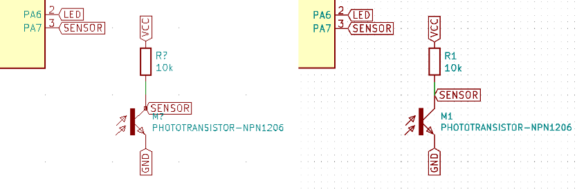
I went ahead and created labels to connect all the remaining end points / pins through labels, which was still something we could find in the schematic we received from Henk (almost forgetting the sneaky SENSOR label on the phototransistor):
This video from the Digi-Key tutorial series in KiCad is truly exceptionally good in explaining all the steps that I took to create my schematic in more detail.
Annotation
Right now all components still have a “?” next to their reference designator. The reference designator is the one or two letter code with which to identify a component on the board. This table on Wikipedia shows the most common codes used, such as R for resistor and C for a capacitor. The “?” is the index of the component; if there are 3 resistors, then they will be named R1, R2 and R3 to distinguish them. Now that I have all the components on my board, I can have them numbered/annotated automatically.
Click on the Annotate schematic symbols icon along the top bar. This will open up the Annotate Schematic window. Here you can make some changes, but I kept all radio buttons to their default position. Click Annotate and KiCad will output what it did (and if it encountered any errors) in the Annotation Messages window.
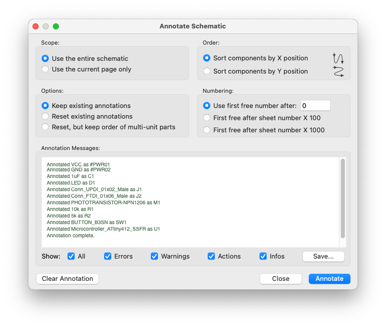
If all looks good, press Close and all the “?” have been replaced by numbers.
Electrical Rules Check
Right next to the Annotate schematic symbols button is the Perform electrical rules check button (looking like a ladybug). Clicking this will open the Electrical Rules Checker window. It’s empty first, but click Run and KiCad will check the schematic for errors.

Besides these errors, you’ll also get small green arrows at the connections in the schematic, such as the VCC, GND, and SENSOR in the image below:
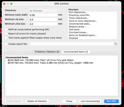
At first I actually didn’t really do anything with this and ignored the results. Until I saw that I was missing a connection from my sensor to the microcontroller while in the PCB Layout Editor. I remembered that the rules checker had given an error for that pin, and thus I went back to see if something was wrong. The error message was quite vague, so I decided to google for phototransistor npn1206 to see if I could find an example schematic and how the sensor label should be attached.
Thankfully, I found the documentation page of a previous Fab Academy student in which I saw that their label was placed higher than mine. I also noticed that in my schematic, the sensor label also still showed a circle, meaning that it’s not actually connected to anything (image below left). I moved the label up to the top part of the phototransistor’s symbol, and now the sensor label did attach and the circle removed (and the electrical check error had disappeared). In the PCB Layout Editor my missing line was now there thankfully.
Seeing as how that fixed a true error in my schematic, I wanted to try and fix the other errors as well. I saw that two related to the fact that two pins of the FTDI were unconnected. I googled the error message that I could add a “no connection flag” to them. This showed me that there is a Place a no connection flag button along the right (a blue cross). I added two crosses to the FTDI pins and this did indeed remove those two errors from the electrical check.

The final two errors had to do with “Pin connected to other pins, but not driven by any pin”. I checked the documentation from a student from last year, Tessel, that Henk recommended we check out in general for this week. I read that she had the same errors. It had to do with the fact that there was no true power source in our schematic, because the FTDI would supply the power.
Although Henk had told her to ignore these errors, which I did at first as well, I eventually found a solution. The Electronics Design video of Aalto Fablab was shared within the Global Open Time Mattermost channel, and at 37:48 we see exactly how to place power flags.
Click the Place power port button along the right and click anywhere on the page. In the Choose Power Symbol window that pops up search for PWR_FLAG, select it, and click OK.
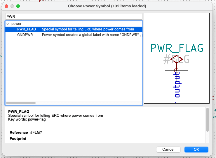
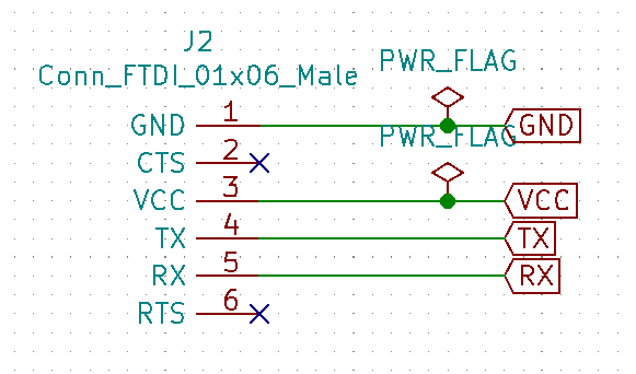
Now click on either the VCC or the GND pin of the FTDI to attach it. Repeat the step for the other pin (I moved the labels a bit to the right so the PWR_FLAG words weren’t overlapping the other text as much). It should now look as follows:
And that was it, when I ran the electrical rules checker again, it was all good, no more errors! (๑•̀ㅂ•́)ง✧
Assigning Footprints
Now we go one more button to the right. We need to assign the schematic symbols with footprints to be used on the actual PCB. Click on the Assign PCB Footprints to schematic symbols icon along the top. After a quick load this will open up the Assign Footprints window that will show all the symbols/components that we’ve used. Thankfully the Fab library is well made and each component is already connected to a footprint (you can see this because all the rows have the Assignments value filled in). It doesn’t hurt to check if all this is correct.
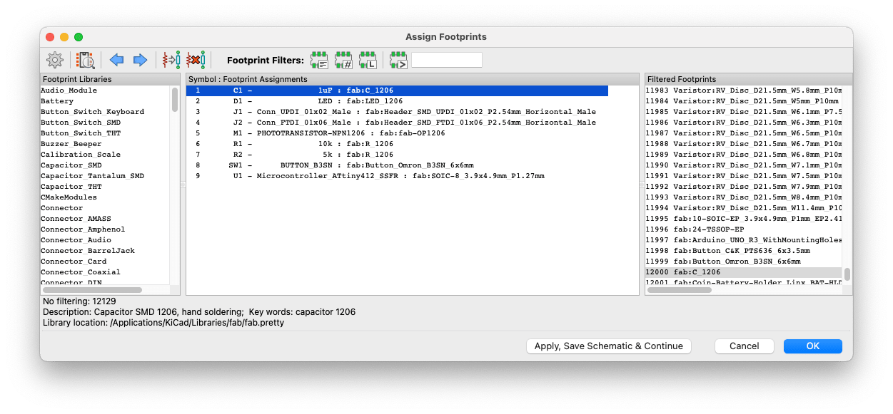
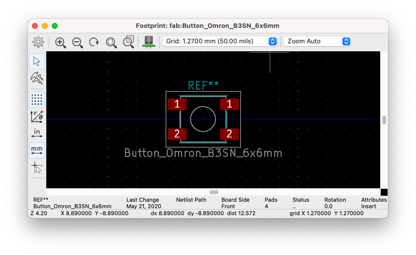
If you’re not sure about a part, it might help to view its footprint. To do this, select the row of the component to inspect and click the View selected footprint button along the top-left of the Assign Footprints window (with the little magnifying glass). This will open up yet another window showing the part. Such as the image below for the button:
If it’s all looking good, press Apply, Save Schematic & Continue, and then press OK to close the window (don’t forget that important first button though to actually apply the footprints).
Generating a Netlist
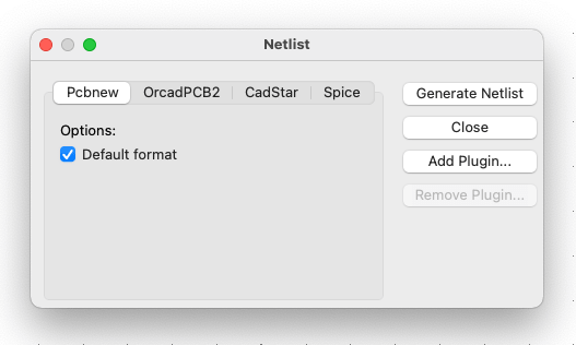
Finally, we’ll generate a netlist, although I’m not quite sure if is truly still needed, because we can use the Update PCB from schematic function in the PCB Layout Editor. A netlist is a file that describes which pins/ports are connected to which. Click the Generate netlist button at the top. It lists the components in the schematic and the nodes they are connected to. We’re staying within KiCad so we can just stick to the Pcbnew and click Generate Netlist. Save the file (in the same directory as the project for example).
For an extended explanation of the annotation, assignment of the footprints, and netlists, watch this video, that shows some of the handy options and filter functions in the Assign Footprints window in case not all schematic symbols have a/the correct footprint assigned to it.
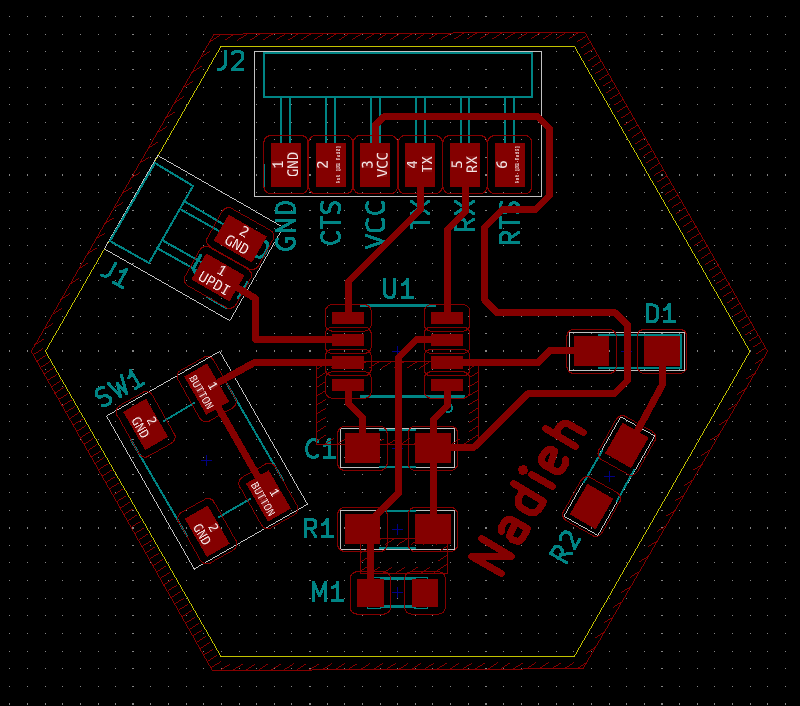
Final Schematic
And with that my step within the Schematic Layout Manager was done. Below you can see my final schematic:
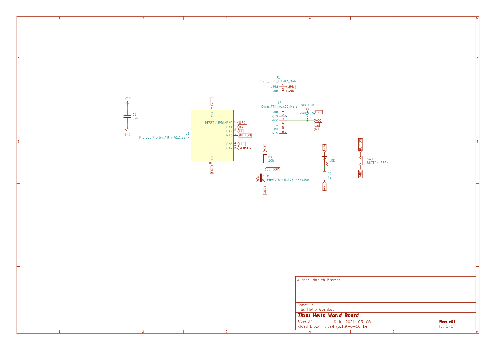
And these are the components that are in it:
| Component | Full Label | Name on Box at Waag | Reference Designation | Specific Orientation |
|---|---|---|---|---|
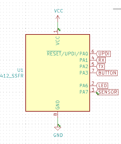
| ATtiny412 | Microcontroller_ATtiny412_SSFR | ATTINY412 | U1 | Yes - Dot in one corner |
| UPDI | Conn_UPDI_01x02_Male | CONN HEADER SMD | J1 | Yes |
| FTDI | Conn_FTDI_01x06_Male | FTDI Header | J2 | Yes |
| Button | BUTTON_B3SN | SWITCH 6X6mm | SW1 | Yes - Lines along the bottom |
| Phototransistor | PHOTOTRANSISTOR-NPN1206 | PHOTOTRANS. NPN PLCC-2 | M1 | Yes - Triangle cutout of collector side |
| LED | LED_1206 | LED BLUE | D1 | Yes - “T” shape pointing to cathode |
| Capacitor 1uF | C_1206 | CAP 1uF | C1 | No |
| Resistor 10kΩ | R_1206 | RES 10K Ω | R1 | No |
| Resistor 5kΩ | R_1206 | RES 4.99K Ω | R2 | No |
I saved the result one more time and closed the Schematic Layout Manager window.
PCB Layout Editor
Back in the main window of KiCad, press the PCB Layout Editor button (the brown/green icon that looks like the traces on a PCB). I need to add the footprints of the components in the schematic and draw actual traces between all of them. A footprint is the arrangement and physical dimensions of the pads or through-holes used to physically attach a component to the PCB.
An empty black overview appears on which to place the components (you could change the metadata in the lower right section again by going to File -> Page Settings). Below you can see the main functions that I used while in the PCB Layout Editor that I’ll be referencing in this section.
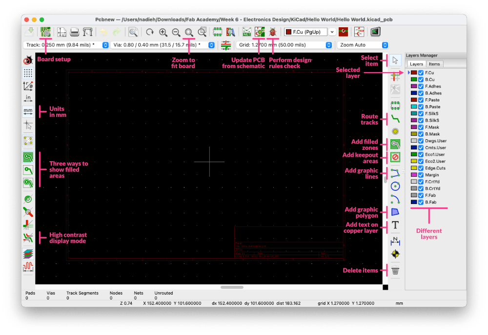
From the KiCad tutorial series that I keep referencing, it was part six and part seven that helped a lot to learn more about creating a PCB layout.
Design Rules
Before I truly start to try and create a layout of my PCB, I need to set the Design Rules, which are the limits of the milling machine, in terms of its precision and milling diameter. This helps prevent me from putting components and traces too close to each other in KiCad.
Click on the Board Setup button along the top to open a new window in which to update the design rules of the Roland Modela milling machine.
I checked the documentation of Henk to see the design rules that he used before:
- In the Design Rules tab I changed the Minimum Track Width to
0.39mm.
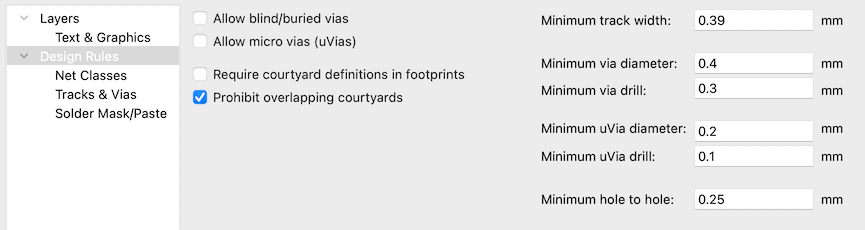
- In the Net Classes tab I changed the Clearance to
0.4mm, the Track Width to0.39mm. I also had to update the dPair Width to be at least as big as the Track Width, otherwise I got an error while trying to save the rules.
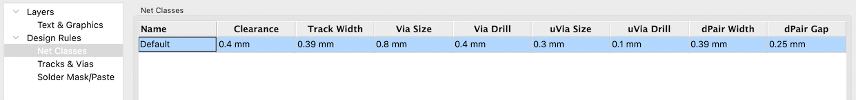
Because we don’t work with vias (our board only has copper on one side) I ignored all of those settings.
Back in the main PCB Layout Editor view I now saw that the “Track” dropdown that is in the upper-left of the page was showing Track: 0.390mm (15.35 mils).
Loading the Components
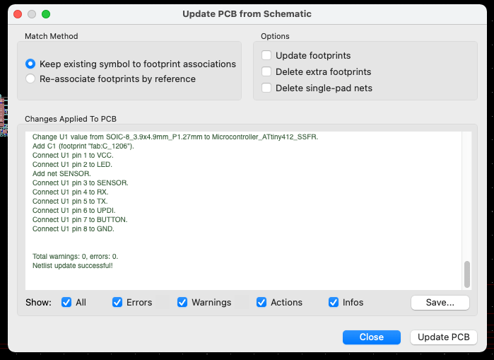
With the design rules set, I need to load the footprints of my components following the schematic I created. Thankfully, there is the handy Update PCB from schematic button at the top. Clicking it will open a new window. I pressed Update PCB and could see that the notes in the central window had updated and that everything went successfully.
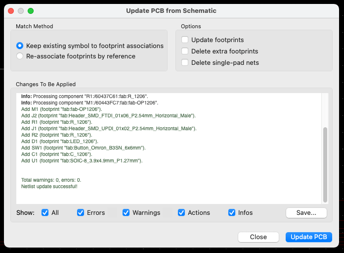
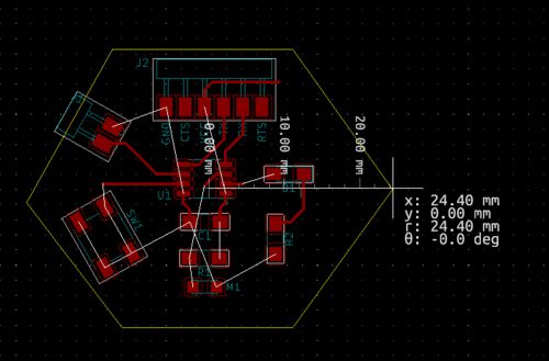
After closing the window I saw that a tight bunch of components had appeared on the page:
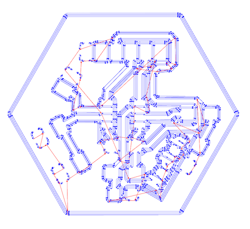
Cleaning Up the Rats Nest
This is quite a mess and won’t work as a practical PCB; crossing lines aren’t allowed. These components need to be moved manually to create a functional layout.
As before, you can move and rotate components, while hovering over a component, with the M and R keys. However, you first need to have the component selected by clicking on it, or have no component selected for this to work.
The white lines are called air wires and help you see which sides of components should be connected. At this point it’s called a “rats nest”, because the wires are going everywhere and crossing many others. I have to untangle them as much as I can, and preferably have no crossing air wires.
I saw in Henk’s documentation that he’d used Freerouter to help him with this routing problem. However, I remembered Neil mentioning that we should be able to do this ourselves. I saw in another student’s documentation that the installation (on Linux) was quite a pain. And while I googled for how to do auto-routing on a Mac I basically only found results about how you shouldn’t auto-route. Thus I figured it would be good exercise to do the routing myself.
Tip | At the top of the PCB Layout editor there’s a drop down to set the Grid (size). This will update how far apart the grid points are, and what the components will snap to. I adjusted this at the start from the default 50.00 mils to 10.00 mils to get more control over the placement. I later found out that the bottom option Edit user grid… lets you choose your own distance. I used this for the fine-tuning of the mask edge points to a 0.005mm grid size, but I’ll get to that later.
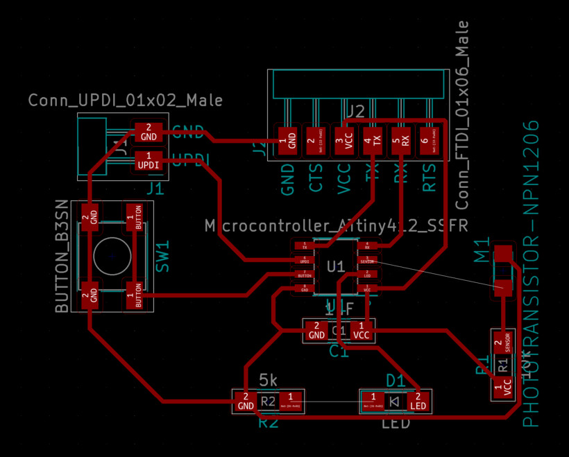
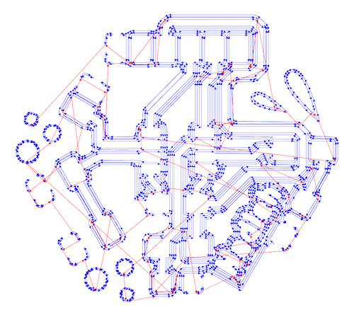
Thinking about how to untangle the rats nest, I placed the ATtiny in the center and wanted to try and get the other components in approximately the right direction to where they should be connected to the ATTiny:
- FTDI: I noticed that the TX and RX legs of the ATTiny were both at the outer edge. I therefore placed the FTDI in the right orientation and close to that side of the microcontroller.
- UPDI: Moved the UPDI connector to the left side
- Button: Moved the button to the left side, but below the UPDI.
- Capacitor: I had read that the capacitor should be placed close to the microcontroller, so I put it right below the bottom side of the ATTiny, where its VCC and GND labels were (I guess this is officially the “top”, but I’m referring to sides as to how they appear in my window).
- LED: I wasn’t quite sure what I wanted with the LED, perhaps some interesting location such as the middle-ish?
- Phototransistor: At the start I thought that perhaps the LED and phototransistor should be placed far away so the LED wouldn’t interfere with the LED (I later asked Henk who told me that they don’t interfere because the LED shines upward).
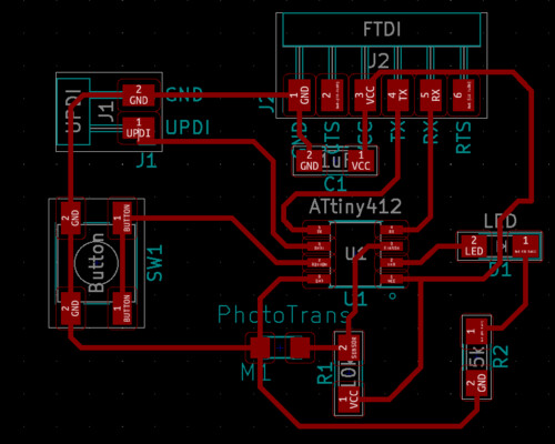
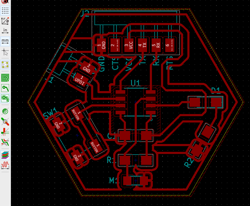
At that’s about how I came up with the result below:

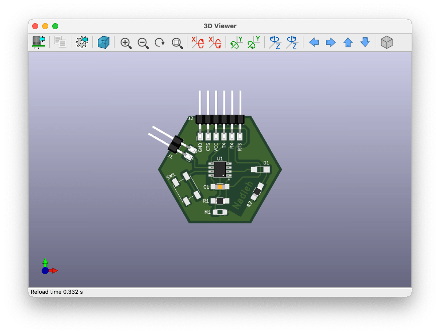
3D Viewer
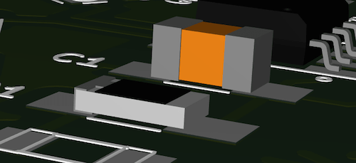
A nice thing to do is to check the 3D view of how the board would look with the actual components on them. Within the PCB Layout Editor go to View in the top menu and then select 3D Viewer.
I did this a few times early in the process to see how the legs of the UPDI and FTDI looked, because part was missing from their footprint (the pins sticking outward).
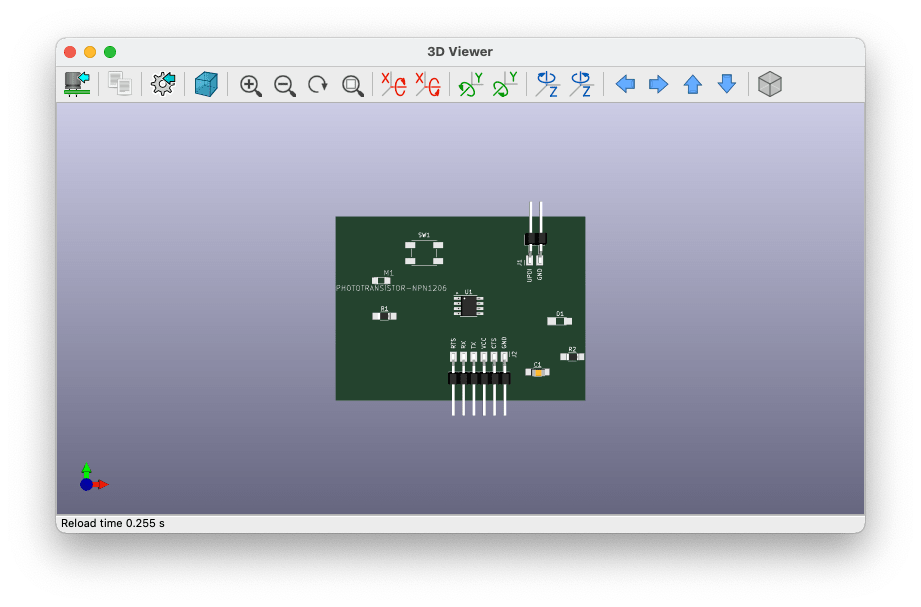
As you can (perhaps) see in the image above, not all the components have 3D counterparts in my KiCad; the button, phototransistor and LED are missing and only showing their pads.
Drawing Traces
After fiddling around with the components for a bit longer and trying to imagine how traces might be placed, it as time to actually draw them!
Click the Route tracks button along the right (green line). By default this will draw horizontal, vertical or 45° lines (having to do with “acid traps” occurring in small angles with the way PCB used to be made, but this isn’t an issue for us / doesn’t happen with the current production processes).
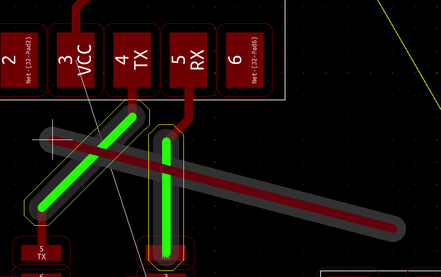
KiCad will make sure not to have any crossing traces: if you’ve drawn a few traces, and draw another one where the shortest path would cross those, it will put the line around the traces. See for example the VCC line below, going around the TX and RX trace I placed to the ATTiny.

I often found myself in situations where everything seemed to be going well except for one final trace, such as the one below where I couldn’t place the final connection between the phototransistor and the ATTiny along the middle-right.

And two more attempts that failed at the last connection:
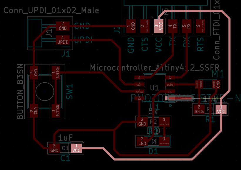
Finally though I figured that I had to route more lines underneath some of the components, using them as bridges, which finally resulted in a design in which I managed to connect all the lines (๑•̀ㅂ•́)ง✧
However, I wasn’t quite happy with it, because one of the traces was going under the phototransistor, which had the smallest bridge of basically all components. I therefore kept on tinkering with the positions of the LED and phototransistor (and their resistors), and found several other solutions.

To check if I hadn’t forgotten any part, I click the Perform design rules check button along the top (the ladybug) and pressed Run DRC. If all is good, you’d see nothing in the central text area. But because that’s a bit uninteresting, below is an example in which I removed one trace to see what the error messages might be:
Throughout the process of placing, moving and deleting tracks I easily got frustrated with how much work it was with only using the buttons along the right: if I moved a components I had to delete each piece track to it, and then draw new ones, but the Delete items button would often deactivate if it wasn’t sure what I’d clicked. Thankfully, after watching a bunch of tutorials, I had gathered a bunch of really useful short keys to make life much easier:
- Hover over a track and press
Backspaceto delete the segment. If you hitDeleteit deletes the entire segment apparently (but I don’t have that button, so I can’t test it). - Hit
Dwhile hovering over a track will move the track segment without it losing its connection to other tracks, and will also move tracks away that you’re bumping into. - Hover over a trace and hit
U, this will select the entire trace. You can then hitMto move the entire segment. HittingIwhile hovering over a track will select all the connected traces and segments. - Hover over a track, label, component, pad, basically anything and hit
E. This will open up the Properties window and lets you adjust a variety of things, depending on the type of item that you hovered over.
I gathered the following lessons about how to place components and think about trace order (I gathered these along the way, so some layouts below aren’t yet following these rules):
- Make sure that the VCC and GND of the microcontroller is connected to the point of power through the capacitor. In this case that meant placing the capacitor in between the lines going from the FTDI to the ATTiny.
- Try to connect any communication line first, and keep these short. In this board those were the UPDI line of the UPDI connector, and the TX and RX lines of the FTDI connector.
- Next, try and connect the other lines to the pins of the microcontroller. Being the button, LED and phototransistor for this board.
- Or, route the VCC lines (I don’t think there’s a specific order to this one or the previous one).
- Connect the GND traces last (or do a “copper pour” which I’ll explain farther below).
Adjusting Labels
Now that I had at least a functional PCB in terms of traces, sort of completing a first spiral, I wanted to fine-tune my design and clean things up a bit.
I was annoyed that the names of the components on the PCB were so incredibly long. By pressing E while hovering over a label I could indeed adjust the text. However, I noticed that it would revert back to the old text as soon as I did another Update PCB from schematic. I guessed I had to update the label in my schematic.
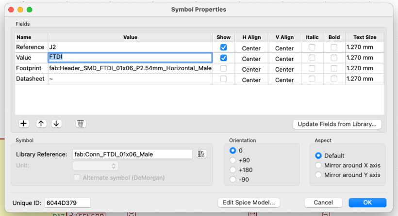
Back in the Schematic Layout Editor, I hovered over a component and pressed E to open up the Properties window. In there I changed the Value field of the long-named components to something shorter, such as FTDI instead of Conn_FTDI_01x06_Male.
Back in the PCB Layout Editor I pressed Update PCB from schematic again, and this time all the (white) labels updated to how I set them. Using M while hovering over a label, I moved them around a bit to be placed either within or just above it.
I never figured out why the phototransistor had a different font color and size as the other labels (in white). But by pressing E while hovering over it I could adjust its settings to be the same as for the white labels.
Edge Cuts
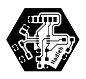
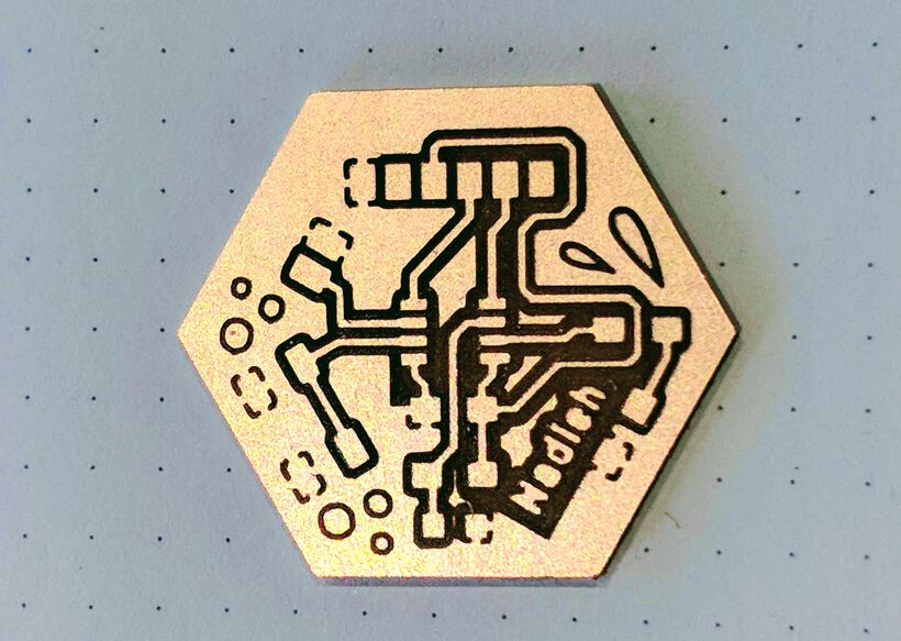
With the labels fixed, and having time left in my Sunday I thought about what kind of PCB I truly wanted to create. Perhaps I could try a slightly non standard form (but not too crazy, this was still too new for me), so I would learn more about using KiCad? And I also wanted to have the LED placed somewhere at least somewhat special.
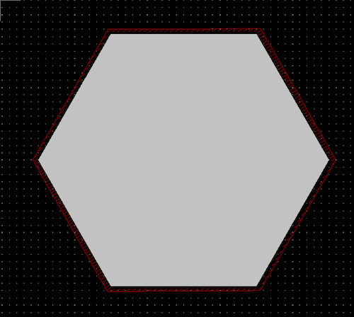
Seeing as how I love hexagons, I figured that would be a good shape to try, with the LED somewhat singled out/placed in one corner of the shape.
I first drew a rough shape of a hexagon around my components. To do this, make sure to first select the Edge.Cuts layer. Next, click on the Add graphic lines button along the right (green dots with blue lines). Since I knew that I could adjust the exact positions of the corners of the edge cut polygon, I just drew a really rough hexagon around it all, to get a sense of how it would fit.

As before, I could hover over a yellow edge line and press E to get the lines' properties and place each end point exactly (I did have to zoom in quite far to actually have the hover-over-line be picked up).
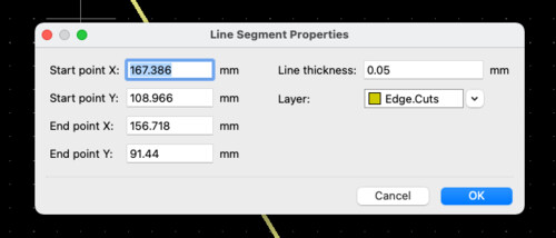
To make it easier to calculate, I placed the right-most point on an integer position of 170,110. I then used the Measure distance tool (the caliper button along the right) to measure the distance between that point and the center, which was about 25mm.
This gave me all the info I needed to calculate the other positions of the hexagon using some simple trigonometry (e.g. the center of the hexagon is at 145,110, thus the top-right corner is at 145 + 25 * cos(30°), 110 - 25 * sin(30°)). However, that made the hexagon much larger than was needed, thus I adjusted the coordinates to fit with a 20mm radius instead.
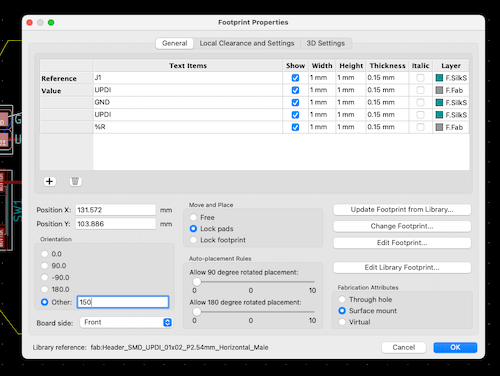
As you might see in the image above, I’d also rotated the UPDI and the Button along the left to be in line with the outside edge. This is yet another property that can be adjusted by pressing E while hovering over the components (not a pad or a label) and adjusting the Orientation (in the lower left) to Other and giving a value:
Free Angles for Traces
Now that some of my components where at odd angles, I wanted to draw some of the traces being parallel to them. However, the default only lets you draw horizontal, vertical or 45° lines. A quick online search showed me the solution. While the Route tracks button is selected, right-click anywhere and choose Interactive Router Settings…
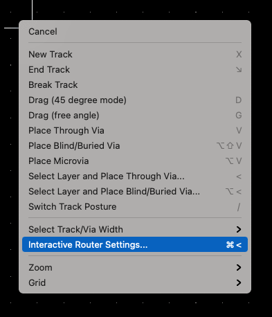
Within the window that pops up, switch from Walk around to Highlight collisions, and then check Free angle mode.

In that case you can draw a line straight through other traces (at any angle), but any crossed lines are highlighted in green.
You can’t snap the traces anymore while in this mode (i.e. if you want horizontal or vertical traces you’ll have to eye-ball it), so I wouldn’t recommend the free angle mode in general. I only placed a few of the traces in this mode; the one running from the UPDI and Button back to the ATTiny, and later a small section from the resistor to the LED. The rest I did with the normal mode.
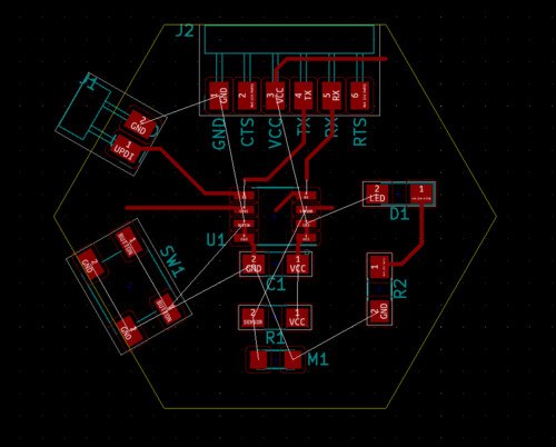
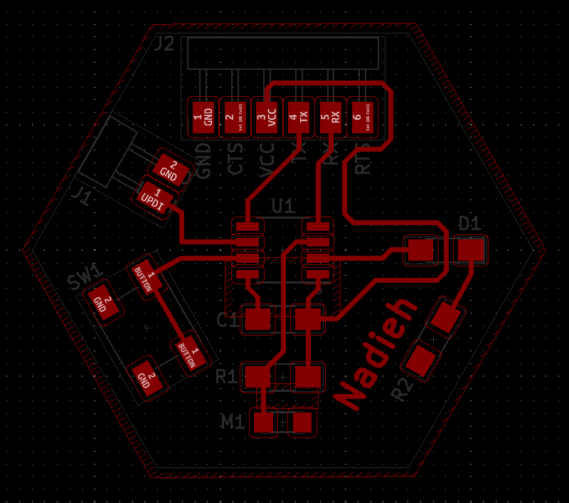
Eventually I ended up with the following layout:

Filled Zones for Ground
Around this point the (really great) video tutorial by Aalto Fablab on KiCad was shared in the Global Open Time Mattermost channel. From that I learned a bunch of useful things, one of which was to use/leave a so-called “copper pour” to make all the rest of the (connected) copper on the PCB into GND.
Because I’d watched the tutorial, I already knew that I had to make a Keepout Area around the microcontroller. Specifically to make sure that the GND (but also VCC, however that would be go correctly even without the keepout area) of the ATtiny only connects to the general ground through the capacitor.
Click the Add keepout areas button along the right and click where you’d like to start drawing the polygon. One the first click you’ll get a window that asks what kind of area you’d like. Make sure to deselect Keep out tracks and select Keep out copper pours (and only have the F.Cu layer selected).
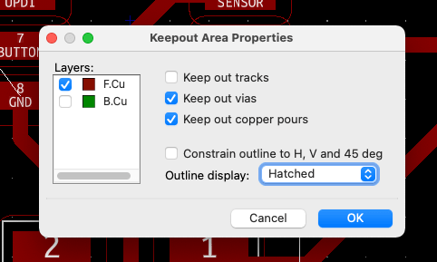
Draw the area you want. It doesn’t have to be precise at first, you can always select each side and corner and move it later. I initially drew my keepout area around the full microcontroller, including just the top part of the capacitor. The hatched area shows where that area is.

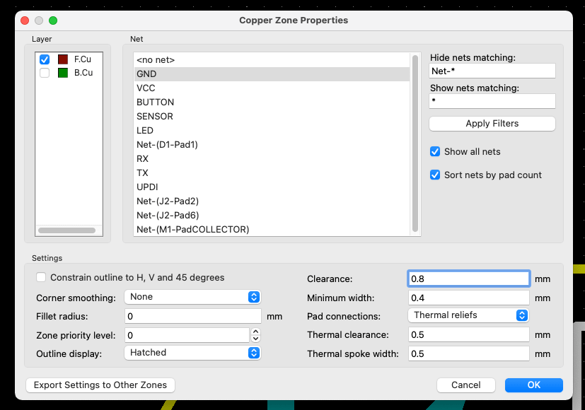
Next, I could add the “copper pour”. Click on the Add filled zones button along the right. Make sure the F.Cu layer is selected. Click about where you’d want to have the copper filled area. The Copper Zone Properties window will pop up. Make sure the F.Cu layer is checked. In the Net box select GND. This will make all the GND pads to get connections to the copper area we’re about the create. Finally, in the lower-right make sure to adjust the settings:
- Clearance | This is the distance between the filled area and any other part that isn’t a GND pad (and the edge of the board). I could’ve used
0.4mm, but just to be sure I set it to twice that. - Minimum width | I used the
0.4mmthat is the minimum for our milling machine’s smallest drill. - Pad connections | How should the GND pads be connected to the copper filled area. In its most simle form you don’t need actual pads anymore. However, that makes soldering really difficult: you can’t heat up a small area, because the heat dissipates into the entire connected copper area, plus it’s hard to position your components, because you’ve visually lost some of the pads. It’s therefore better to set them as Thermal reliefs. In that case a small area is still removed around each GND pad, but (if possible) each pad has 4 tiny connections to the outside copper area (you can see this better in the image farther below showing the results).
- Thermal clearance | The thickness of the area that gets milled away around each GND pad.
- Thermal spoke width | The thickness of the (max) 4 spokes with which the GND pads are connected to the copper area. For these numbers I followed those that were used in the tutorial from Aalto Fablab and set them both to
0.5mm
This tutorial on creating copper pour fills in KiCad also explains a little more about all the settings in the Copper Zone Properties window.
With the settings filled in, I drew a rough hexagon just outside the board edge. This doesn’t need to be perfect, because the copper area will not go beyond the board edge. But I can always move the corner points around afterwards.
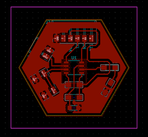
At first I thought I did something wrong, because I wasn’t seeing any copper area as I saw in the tutorial video. However, I then found that there are three different options to see any filled area. You can switch between these with the three green buttons (with a circle and a line coming from it) along the left of the PCB Layout Editor screen. The Show filled areas in zones is probable the most useful to get a sense of how the actual copper plate might look, and where you can see the GND pads being connected through those spokes:


I usually had it set to not show the filled area though, because the red is hiding so much.
As you may be able to see in the images above, but the copper area doesn’t go all the way to the edge of the board. This is a precaution for when copper plates with more than 1 copper layer are used (the edge could result in shorts, connecting layers). I tried to find a solution for this, but it appears that there’s no way to have a separate clearance between the board edge and the inner traces and pads. I did find that “KiCad 6 will have a dedicated edge clearance”, so hopefully in some time it will be possible. In my case it meant that I had to do some adjustments in Illustrator with the SVG later on.
Throughout the minute fine-tuning I played around with the exact position of the keepout area, and also added another small area between the phototransistor and its resistor so it would look nicer. Making changes to the board doesn’t always update the copper area. To update the copper filled area, press B.
Tip | A useful option that I only discovered near the end of my work with KiCad is the High contrast display mode. Press this button along the left option and it will mute anything that isn’t a trace or a pad, making it much easier to focus on those parts of the board while you’re drawing traces.
Adding a Margin
Another thing I learned from the Aalto Fablab tutorial; it’s better to add a margin around the board of 1-2mm because it makes it easier/possible for mods, the tool that will calculate the milling path, to create the outline.
I had noticed this while Henk was giving an introduction to KiCad at the start of the week. I had followed his steps along and created a simple rectangular board. When I saved the SVG, I noticed that the edge cuts svg file had its line all the way at the outside. At first I wasn’t even sure there was a line in the file, and opened it up in Illustrator to check (but yes, the line was there indeed):

I remembered how mods hadn’t cut out any line that was at the edge of my file during the vinyl cutting week, so when I saw this outline being all the way to the outside of the svg, and the Aalto tutorial mentioning that the margin was a good idea, I followed along to make a margin.
However, while I was writing this documentation I wanted to try and see what would happen when I went through mods, so I could describe it. And when I used that simple rectangular edge cut file, from the PCB version I made while following along with Henk, to test in mods it all seemed to work fine. I loaded the SVG, inverted it, and mods had no trouble turning it into a toolpath. So perhaps adding a margin isn’t actually needed (*^▽^*)ゞ But at least it didn’t seem to have any negative side effects, and if I do somehow run into an issue in the future with the edge cuts, I know how I might fix it.
So let me explain what I did and how you can add a margin.
Select the margin layer from the list along the right. Next, select the Add graphic lines button along the right (that we also used for the edge cuts lines), and draw a rectangle around the shape. That’s really it! When you next save an SVG the file runs to the edge of the margin, not the edge of the board. I realized that you need to make sure the margin layer is active/visible, otherwise it will not be taken into account. (You can see the margin part explained in the Aalto tutorial at ±1h02m)
Adding Text & Graphics
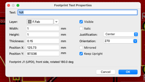
To add useful information, or to just make the board look more fun, you can also add text and graphics to the board. When you’re creating board for a company to make, you can often make use of the Silkscreen layer. This is a white layer that gets printed on top of the board. You generally place the reference designation names of your components so you know what pad is supposed to hold what component.
Adding Text
However, we only have the copper layer, and only the mill to “draw” our graphics. Text is thankfully easy to add to the copper layer in KiCad. Well, in case you’re satisfied with the default KiCad font, because there’s only one available.
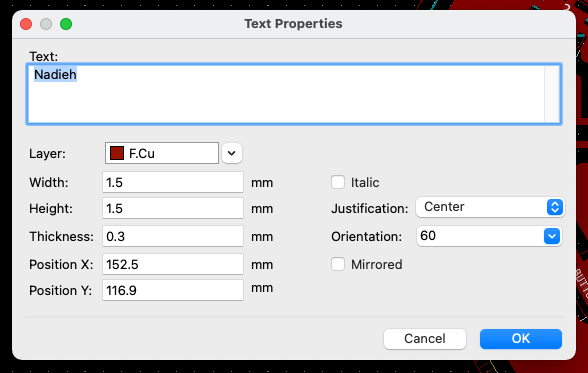
To add text to a copper layer, make sure the F.Cu layer is selected and press the Add text … button along the right (the big “T” icon). Click anywhere and a Text Properties window will pop up. Write the text you want and adjust any of the text size, thickness, font style, and orientation properties. After you click OK the text will “float” under your cursor and you can place it anywhere. As with all other parts, you can always hover over the text and press E to see the properties window again to make changes.
Because I had the copper fill, I had to press B again to update the layer, so it would take the text into account.

Adding Graphics
At first I wanted to add a simple graphic element to some of the empty copper areas of my board in KiCad as well. I discovered that it’s not as easy to do for the copper layer as it is for the silkscreen layer sadly. I did find a few interesting blogs that explain the process. However, I figured that adding a graphic element in Adobe Illustrator afterward would be much easier, especially since I already had to make changes to the SVG that was created for my board anyway (see the mods section below).
Even if I made changes to my PCB in KiCad, as long as I didn’t change the margin I could just load the updated traces layer from the new SVG and paste it into the file that contained the outdated traces (but including the graphical elements) in Adobe Illustrator (removing the outdated traces layer then of course).
Saving to SVG
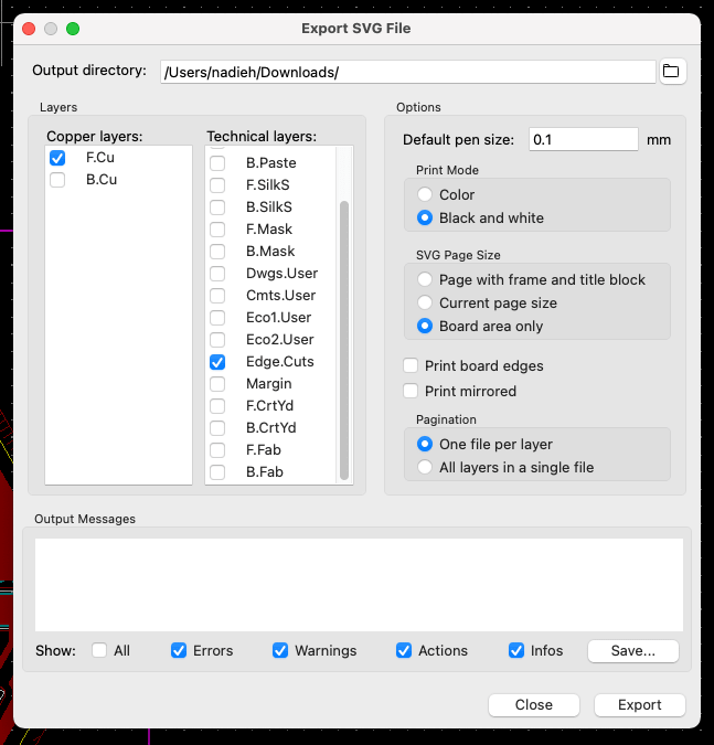
Since the board is now basically done, we need to save it as an SVG file to (eventually) import into mods. In KiCad go to File -> Export -> SVG. Within the Export SVG File window that pops up, make sure to:
- Select the F.Cu for the Copper layer and Edge.Cuts for the Technical layers
- Choose a Black and white print mode
- Choose Board area only for the page size
- Uncheck Print board edges, otherwise the edge will still be present in the traces file (I did this wrong the first time)
- Uncheck Print mirrored (although I believe it’s unchecked by default)
- Choose One file per layer to make sure that the traces and interior become separate files
Interestingly, after having done all the work in KiCad, what you end up making is a “simple” image file (•ω•)

The 3D viewer looked much more interesting, haha.
Preparing for Mods
With my traces and interior SVG files, I opened up mods to check if the toolpath would look correct. I explain the mods set-up in detail in my documentation of week 4. But as a reminder, right-click anywhere and choose open program and then choose MDX mill -> PCB.
Adjusting the Traces SVG
I loaded my traces SVG file, inverted it because mods see white as the color to keep, whereas my SVG from KiCad uses black for that.
However, when I saw the inverted result I realized that it was probably not going to only keep the traces, but also the hexagon outline that was the edge of my copper pour. Which it did:
This wasn’t wrong. It would still create a functional board. However, it would take more time, and I didn’t want to take up the milling machine any longer than necessary, since three other students would be waiting to mill their boards on the day I’d be in the lab.
FYI | If I’d made a trace for the ground instead of the copper filled pour, I would not have had this. I could’ve just inverted the SVG and mods would’ve not seen any hexagon outline.
Removing the hexagonal outline was easy enough to adjust though. I opened the traces SVG in Adobe Illustrator. I added a black background rectangle and a white filled hexagon underneath the black traces to create the following result:
As you can see, I also added a few graphical marks to it; a few circles along the left and two droplet shapes along the middle-right, just to add a little more flair. But I was also curious to see how the milling machine would handle more circular shapes.
Finally, I made the VCC pad of the ATTiny end in a semi-circle. This is something Neil recommended to do as a way to remember what side your microcontroller should be placed onto the board (the semi-circle is where you generally find the marking “dot” on the actual chip).
I saved the result as a PNG file, because then I didn’t have to worry about the exact fills of all the elements I added. There are several ways to save a file in Illustrator, but I used the following: go to File -> Export -> Export As. This lets you set the resolution of the png, which I set to 1000 upon recommendation from Henk. Also, be sure to check the Use artboards option. Otherwise the saved file will save the png to the size of the artwork. If you background rectangle is just a little bigger than the artboard, you might have a traces file that isn’t exactly in line with the interior file (I did this wrong and was off by 2 pixels in each dimension, thankfully I checked the pixel size of the two files and spotted the mistake).
I loaded the updated PNG into mods, inverted it and this time the toolpath looked correct:
Adjusting the Interior SVG
When I tested the SVG file for the edge cuts / interior it also didn’t go correctly. It wanted to mill two traces along the line, whereas I needed one milling path on the center of the edge cut line.

I also tried to not invert the line. However, then no path would show up at all. It also didn’t matter if I had a margin or not. Perhaps the reason why I had no issues with the rectangular board I tried during my test was the fact that this wasn’t a rectangular shape aligned perfectly to the outer edge of the SVG?
I looked at how the interior files looked that we used when we first learned how to mill, such as the basic ATtiny412 board; the entire PCB board area is white while the outside is black.
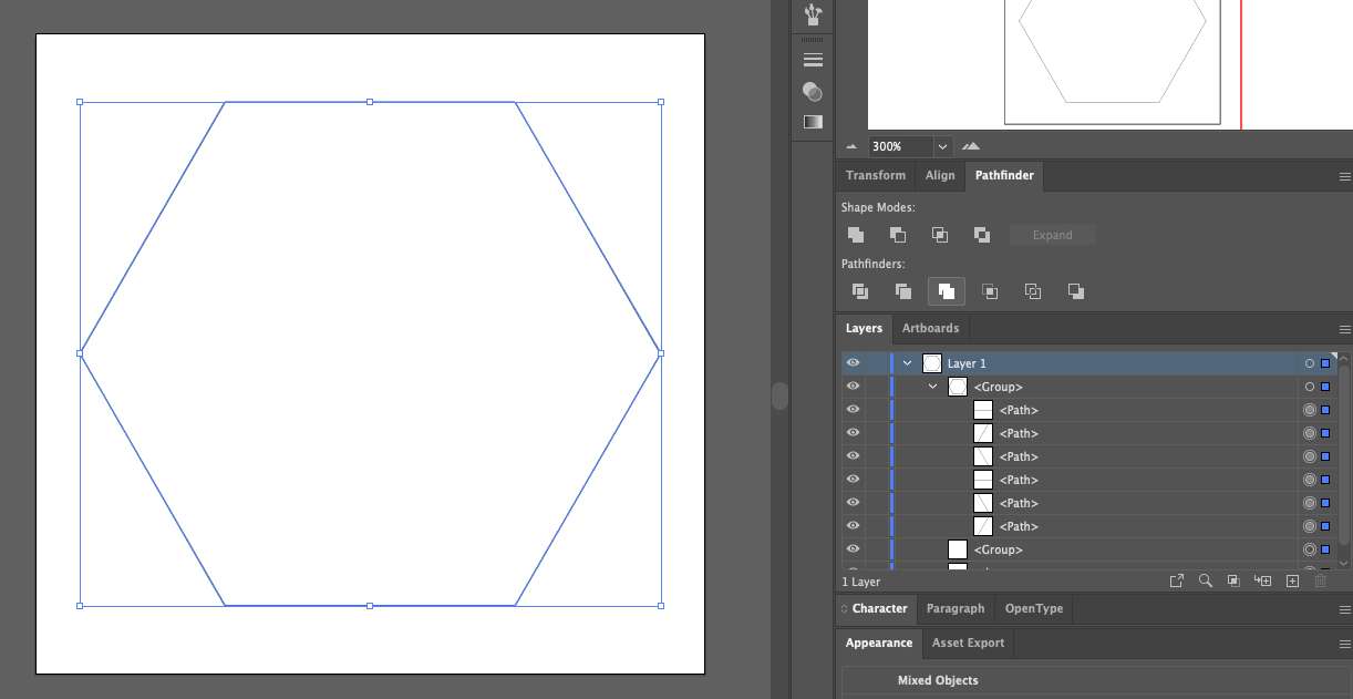
That wasn’t hard to recreate in Illustrator. Sadly the hexagon outline isn’t a shape, but a collection of six loose paths. To be able to fill this with a color I need to join them first: Select all six paths and then in the Pathfinder choose the Merge option.
Afterwards fill it with a white color and set the outside stroke to none. Finally, add a black rectangle to cover the entire artboard (I’m just going to create the “correct” way now, so it doesn’t need to be inverted). And that’s all that’s needed. I saved the result as a PNG and loaded it into mods.

Which resulted in one toolpath being drawn where I needed it to.
A Correct Interior SVG from KiCad
Through the Aalto tutorial I also learned a different method to create a correct interior / edge cuts file straight from KiCad. This is what I ended up using, because I felt it was more practical to skip any possible Illustrator step if possible.
Select the Dwgs.User layer (it stands for “drawings”). Click on the Add graphic polygon button along the right (the blue rectangular-ish shape). Instead of just lines, this will create a filled polygon. Draw a polygon that follows the center of the yellow edge cuts to draw the hexagon.
As before, it doesn’t have to be perfectly aligned on the first try because you can always adjust it later. However, because this is seen as one shape, not 6 separate lines, I found out that I can’t adjust the exact positions of each corner when I press E. Instead it only gives me the option to change the line thickness. Nevertheless, set that line width to 0.
I did find a way to make it work though. When you select the polygon, you can move each corner freely. However, it will always snap to the grid. Thankfully, I can adjust the size of the grid, with the edit user grid… option that’s at the bottom of the Grid dropdown along the top.
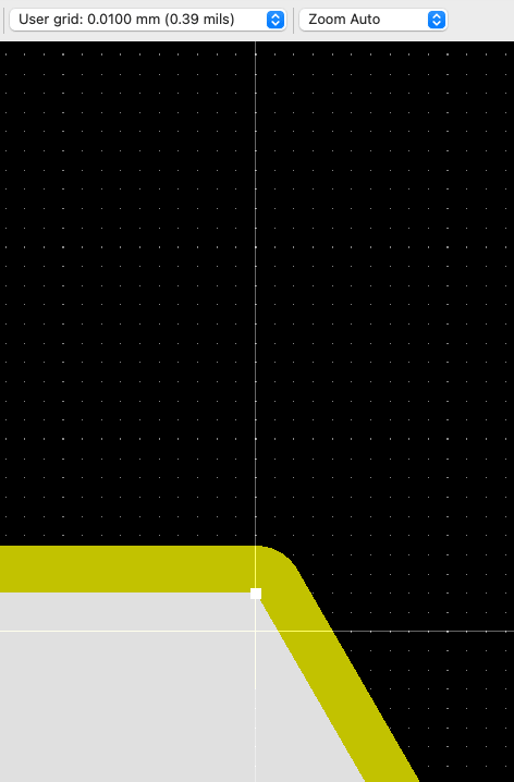
I had used 2 decimals to place the hexagon edge cuts. I therefore set my grid size to be 0.01mm and zoomed in really close to each corner and adjusted the grey polygon’s corners to lie exactly in the middle of the yellow edge cut line.
When doing an export of the SVGs I now need to select the Dwgs.User layer instead of the Edge.Cuts layer. The resulting SVG will be an inverted version of what I need, but I can easily just press the invert button in mods to fix that.

Milling & Soldering
With my traces and interior files producing correct-looking results in mods it was time to actually mill the board! Back in the lab on Monday I set up the Roland Modela machine following the steps I explained in my documentation from week 4.
I did have some weird bug for a bit where I couldn’t get mods to talk to the machine (e.g. changing the origin wasn’t moving the milling bit). The error messages in the console seemed to elude to some deprecated JavaScript code. I was almost afraid that perhaps FireFox had updated during the weekend and now something very small but specific had been changed. I of course followed the “have you tried turning it on and off again” approach, but the same error occurred. I asked Henk to look at it, and he got the error at first too. However, I then couldn’t quite follow what he was doing (he at least checked if the USB cable was actually connected), but at the end the machine was listening to the computer again (^▽^)
The rest of the milling process went smoothly thankfully.


It all seemed to look good. I lightly sanded the top, there were some really tiny burrs here and there, and scraped away a tiny bit of copper that was in between the phototransistor and the resistor (at the middle-bottom of the PCB).
I’d gathered my components in the meantime and was ready to solder. I started with the central ATtiny, making sure to align its marking dot (which is still bloody hard to see) with the bottom right side pin that had the small bump on it.
The resistors and capacitor went next, being so tiny, and having no specific polarity. I did notice that I felt these components barely fit onto the two pads, as if the distance between the pads was too big. Solder it on a little crooked and one side could easily not touch the pad at all!
I checked the 3D view within KiCad to see how it looked there. Perhaps I somehow had scaled up my board a little?? But no, the ATtiny fit really nicely, and the FTDI and UPDI pads were perfectly sized as well. Furthermore, the 3D Viewer showed similarly big pads with only a sliver of connection on either side, so I hadn’t made the PCB scaled up a little.
Perhaps the creator of the footprints made the pads so far apart so it was (easily) possible to have another trace running underneath? Well, it didn’t make the soldering much easier with my shaky hands at least ಥ﹏ಥ
The FTDI connector went on really well, and I could get the solder to flow underneath the connections, merging each pin to the PCB.
The UPDI connector didn’t go quite that smooth. At first I couldn’t find it, because I was looking for two pins specifically. However, Henk pulled out a box with one giant row of connected pins. Apparently you break off the number of pins you need!

And during the soldering I think I positioned the connector just a bit at and angle, because there was a bit of space between the pad and the pins, requiring quite blob of solder to connect the two. No smooth flowing of the solder this time.
The remaining three components had specific ways to solder them on the board that I wasn’t aware of, so I had to do some research before placing each. I checked the documentation of Tessel as a starting point and saw that she’d gone into the datasheets of the components for which she didn’t know the orientation. Tessel had used the same button as I was soldering, so I could use her guidance on that. However, we were using a different phototransistor and LED, so I would have to find my own way for those two.
For the button I knew that internally two sides were connected. I asked Henk if I could place the button a certain way or 180° rotated, and that was the case. Inspecting the button closer I noticed that the connector pads were on two specific sides, that there seemed to be a faint white line running across the center of the button’s top (see image below left) and that along the bottom two raised rectangles were visually connecting two pairs of connection points. All this seemed to clearly indicate which internal sides of a button were connected (here is its datasheet for more info).
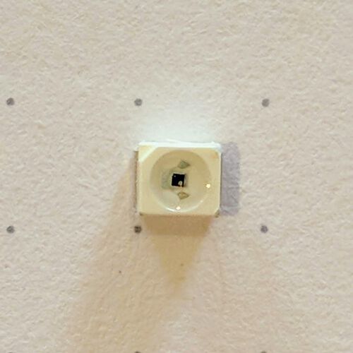
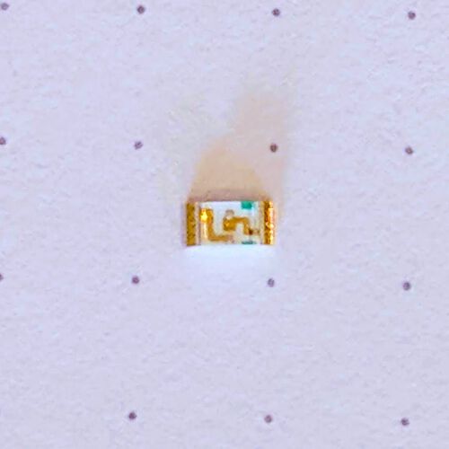
The phototransistor had a triangle eaten out of one corner along the front (there was nothing specific about the bottom).
I looked up the datasheet of the Phototransistor NPN SMD PLCC-2. At first the images in there weren’t really helping me.

I could see that the top ha the corner mark, but I wasn’t sure how the bottom schematic image had been rotated versus the top one. I assumed that side 1 was probably the side that coincided with the top view and the missing triangle, but I wasn’t sure. Also, the words Collector and Emitter were new to me, and I didn’t know which would need to be connected to ground. I somehow missed the schematic symbol on the top-right side, that would’ve given me the info I needed to compare with my schematic from KiCad.
I therefore looked for a datasheet of another SMD phototransistor to look for more clues and found one for the WL-STTW SMT Phototransistor. Here the missing triangle was clearly marked as Collector Mark and this time I did notice the schematic symbol along the right that named the Collector and Emitter:

I compared the symbol to what I had in my own schematic and concluded that the Emitter needed to be connected to GND. I carefully aligned the phototransistor with my board and soldered it on.
Finally, the LED (I picked a blue color). On the back there was a very clear green “T” mark pointing to one side. And on the front I could also see faint green marks along the side (interestingly enough, this wasn’t at the ends of the green line of the bottom it was at the other end).

Searching for “LED SMD orientation” and I saw that several types of back markings are used, such as an arrow (which to me seems to make the most sense from a user perspective since it aligns with the schematic symbol), and that “T” shape. I learned that the middle stick of the “T” points towards the cathode side. And it’s the cathode side that goes onto the GND (I checked with my schematic).
Having soldered on my LED I was (hopefully) done with my board!
I used the multimeter’s continuity test to check the traces and connections of my board. I’m not sure if I managed to check each possible line, however, I did notice that the ground pins of the button didn’t seem to be making direct contact with the copper layer; when I had one pin on a ground side of the button and one on the copper layer, no sound came from the multimeter. Upon closer inspection I could indeed see that the two ground pins were just a little bend upward it seemed, at least, they weren’t touching the plate by a fraction of a millimeter.
I turned the soldering iron back on and tried to add more solder to those two pads so they would make contact with the two contact points of the button. Strangely, the solder wasn’t really interested to cling to the two contact points and I ended up having to add quite big blob of solder to the pads before even a thin connection was made. Perhaps I’d greased up those to pins while trying to inspect in which orientation the button should be soldered onto the board earlier? Nevertheless, the two connections did seem to be working now when I tested them again with the multimeter, so I left it at that.
I asked Henk if I could check anything else, but he said that comes in the Embedded Programming week in two weeks, and that I was done with my board for now ( ^∇^)
Testing the Board
However, on Tuesday evening I checked the Fab Academy’s assessment page and saw that the last line was to also test the board, which Henk had forgotten about (*^▽^*)ゞ I therefore came into the lab on Wednesday morning because I didn’t have a way to connect to the FTDI side of my board, and I had no idea how to test my board.
I got the FTDI from Henk and had to connect both my UPDI and that FTDI board to my Mac (using a USB hub) and also connect them to my hexagon board. The FTDI would only supply the power, and the testing and programming would go though the UPDI:
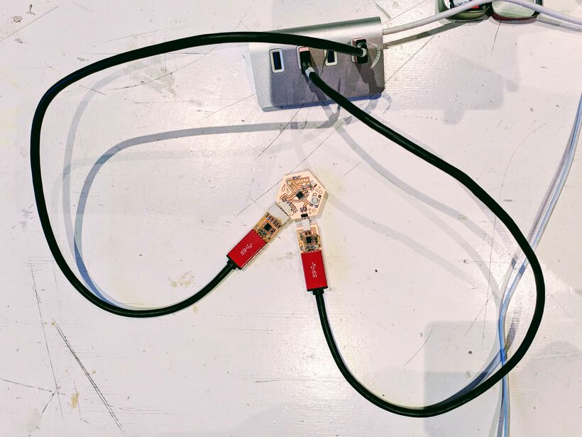
On my Mac, both of these show up as a FT230X Basic UART, so I had to first connect only the FTDI and afterwards only the UPDI and use the system_profiler SPUSBDataType (or ls /dev/tty.*) command to see more information, such as the Serial Number to know which one to use later on.
I then downloaded the Arduino IDE that opens up with a little window in which you can write and compile your script.

Looking at the video from Neil on how to create simple echo test program for the ATtiny412, I saw that we should use his echo.ino code, which I copied and pasted into the Arduino IDE window.
However, when I pressed the Verify button (the check mark top-left), it returned an error about 'class HardwareSerial' has no member named 'swap' not being a recognized function. However, looking closer at the video from Neil, I saw that he was missing the Serial.swap(1); line entirely, so I simply removed/commented it (this came back to haunt me a little later though). This time the compilation was successful.
Getting pyupdi to Work
Continuing to follow the video from Neil, I saw that he ran a line in his terminal with pyupdi. I had already installed the dependencies for this in week 4, but hadn’t actually done anything with it. I did remember that there was something about it on the Fab Academy documentation under UPDI, which was:
# Install dependencies (which I'd already done)
pip3 install intelhex pylint pyserial
# Run pyupdi
python3 pyupdi.py -d your_processor -c your_port -b your_baud_rate -f your_hex_file -v
I downloaded the pyupdi files from GitHub, unzipped them and placed them in my Documents folder.
In case you’re trying to follow along, don’t do what I’m doing below to get pyupdi to work. If only I had scrolled down a little on the GitHub page and had seen the one-line command to install pyupdi with pip3 install https://github.com/mraardvark/pyupdi/archive/master.zip. The next part of this section explains my silly wanderings to get pyupdi to work in a really cumbersome way.
At the start I wanted to test running pyupdi.py. Within the pyupdi folder I ran ./pyupdi.py only to realize that there was no pyupdi.py file in that top folder. The scarce few “tutorials” that I found on using pyupdi all seemed to assume that this file should be in the main folder. I digged into the GitHub commits and saw that they made some changes to the file structure last August. The pyupdi.py file had been moved into the updi folder.
No problem, I tried to run updi/pyupdi.py. This time I got the error Permission denied. At least this error I knew about. I’d come across it a few times during my “life before Fab Academy”. I checked the permissions of the files in the updi folder and saw that they had to execute permission. To quickly fix this for the entire folder, I ran chmod -R 777 updi/ to make all the files within the updi folder get executing permissions (I could’ve used 755 also I think).
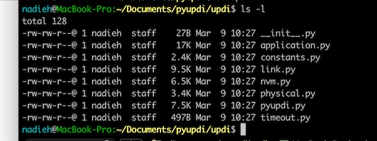
I ran updi/pyupdi.py yet again, and got an error about No module named 'device'
Looking into the actual pyupdi.py file, I saw that it tries to load Device from device.device.
Perhaps it was an issue that the device folder was outside the updi folder? I tried moving the device folder into the updi folder, but that only changed the error to No module named 'updi.pyupdi'. I tried moving the pyupdi.py file one level up, but then got the error ImportError: attempted relative import with no known parent package. I tried copying the pyupdi.py file to the main pyupdi folder instead of moving it, and then it finally seemed to work!
But that just seemed weird, I’m sure the creators of pyupdi would not need me to copy a file to a different folder to get it to work. I don’t know python well enough, so I did the following step on a whim after figuring “Well, maybe there’s something about the setup.py file in the pyupdi folder?”
I googled a bit and saw that I could run python3 setup.py install while in the pyupdi folder. This did a bunch of things and made a bunch of new files in that folder, all of which didn’t seem that useful to me. I therefore threw away the new files. But, afterwards I could run pyupdi -h from anywhere, not just the pyupdi folder. I looked closer at the many lines of output resulting from running the setup command, and saw that those “useless” new files had also been copied over to my local python build (e.g. Copying pyupdi-0.0.0-py3.8.egg to /Library/Frameworks/Python.framework/Versions/3.8/lib/python3.8/site-packages). I guess those files weren’t that “useless” after all (*≧▽≦)
Creating My Own FTDI Board
While all this was happening, I also quickly milled and soldered my own FTDI board. The hello.USB-serial.FT230X to be precise, which is the FTDI counterpart of the UPDI. You can find the schematic, traces and interior on the Fab Academy site.
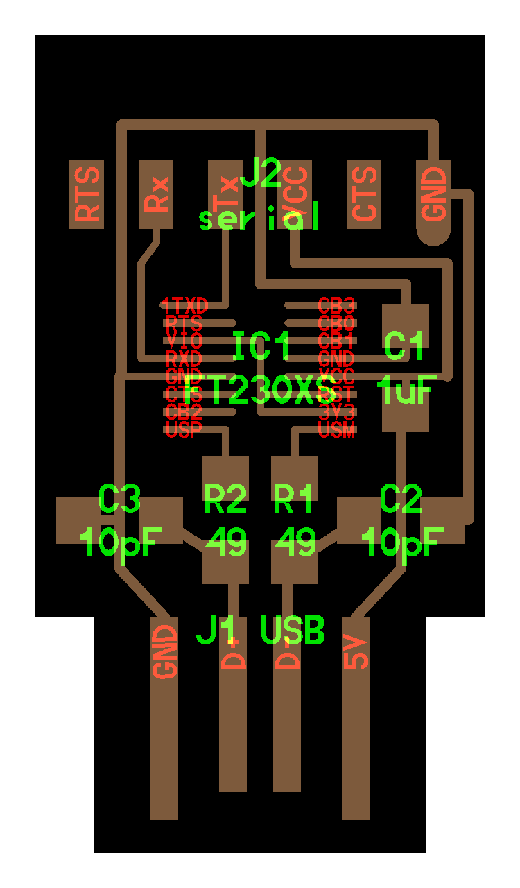
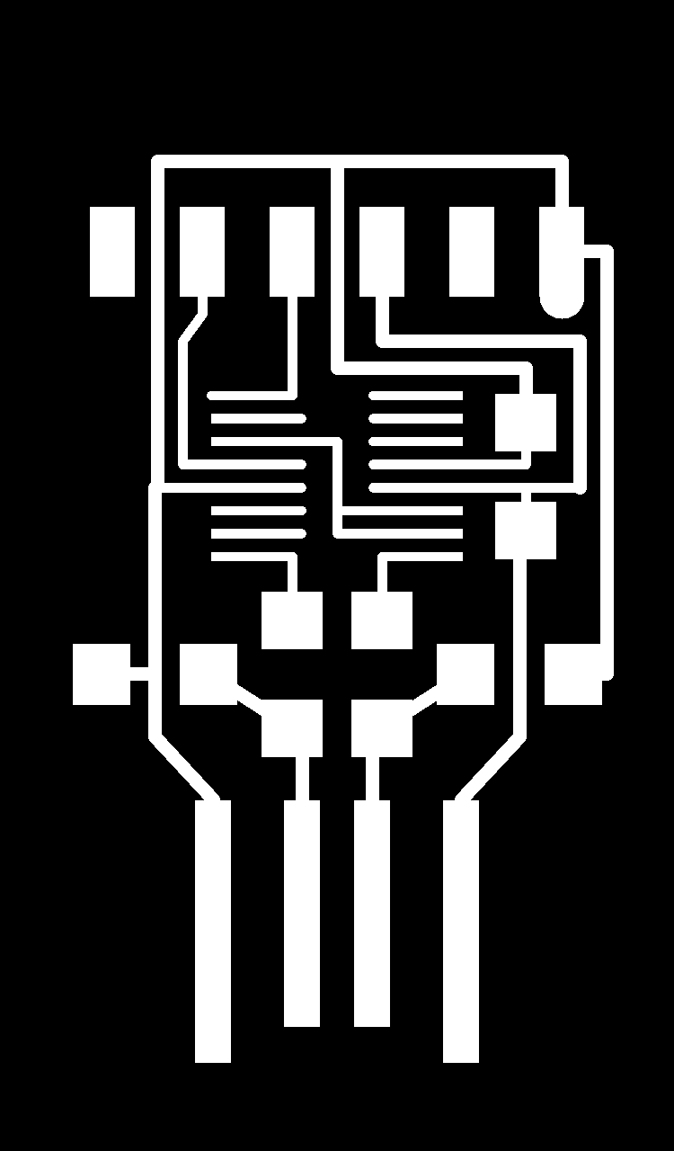
The first milling went wrong, because the milling bit was too blunt, and it had milled off some of the central tiny traces. Thankfully, after replacing the 0.4mm bit I got a nicely milled board.
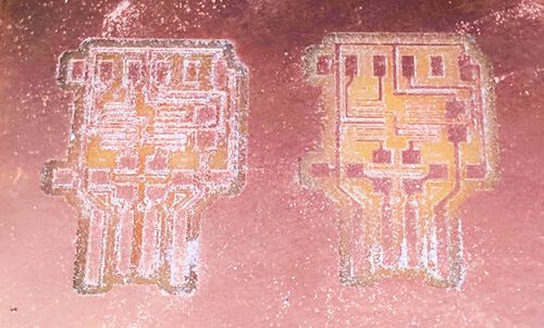
I wasn’t looking forward to soldering that central microcontroller because the pins are so tiny that you can’t solder them separately, but have to solder them all and then remove the excess solder. For my UPDI this had gone pretty painless, but I felt that was mostly luck, especially as I saw how much trouble some of the other students were having with it during that week.
I started out using a heated vacuum pump for the first side. It went well for the bottom half, but it just wasn’t working for the top half. And I almost destroyed a trace along the edge (see the middle-right side in the image below) when I touched the hot side to the edge of my board. I then tried using a cutter to cut in between the excess solder of the top 3 legs, but then the outer two legs moved sideways! (⑉⊙ȏ⊙) I felt like I had messed up my board right then and there… I could bend them back, but I was afraid that I’d destroyed the trace underneath.
However, I checked the schematic and saw that the top three legs are not connected to anything, so it seemed I was in luck!
For the other side (the left side in the image below), I didn’t want to use the vacuum pump anymore, and went for the solder wick. It felt like I had to place the copper wick very specifically to make it suck up the copper? It just seemed to sometimes work and sometimes nothing was happening. But in the end, it was quite effective at removing the excess solder (I did solder my wick to the pins on a few occasions, hehe).
The rest of the soldering went smoothly, and when I plugged the FTDI board into my Mac it was thankfully recognized, so it seemed to have all worked out.

Trying to Program the Board
Getting back to actually using pyupdi to program my board, I looked at that string if info I needed from Neil’s echo video: python3 pyupdi.py -d your_processor -c your_port -b your_baud_rate -f your_hex_file -v.
From Neil’s video I could see that your_processor = attiny412, that your_baud_rate = 57600, that your_hex_file was the file that I got from compiling it with the Arduino IDE. Only your_port I had nu clue about. I tried googling to find out what this was, and how to find it on a Mac. Eventually Henk came to my rescue and said to look at the Arduino IDE under Tools -> Port. Here I saw an entry that had the Serial Number of my UPDI board! I see, so the full port name was /dev/cu.usbserial-D308HTPQ
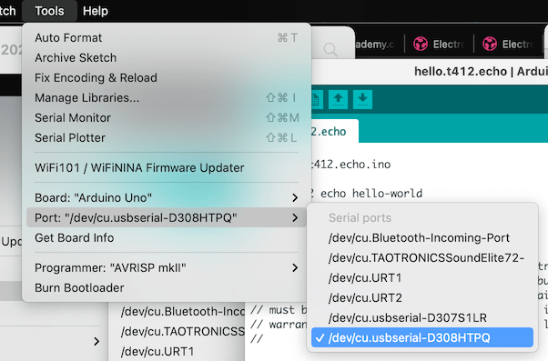
I later learned that I could’ve also used ls /dev/tty.* to get a slightly different version of that port:

With that I figured I’d gathered all the pieces to run Neil’s command in my own terminal (I didn’t have to use python3 pyupdi.py, which only works if you’re in the pyupdi folder, but could just use pyupdi while in any folder):
pyupdi -d tiny412 -b 57600 -c /dev/cu.usbserial-D308HTPQ -f ~/location-of-hex-file/t412echo.ino.hex -v
Running this seemed to start out well, but after a few seconds it would result in an error about how the UPDI initialisation failed (╥﹏╥)
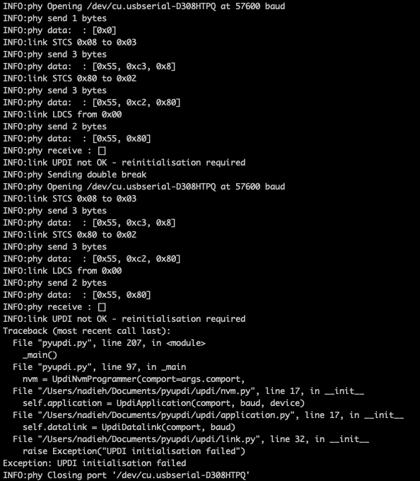
I searched the web for link UPDI not OK, but the results were few and seemed rather varied. I found the documentation from a previous student who had the same error. For him it had been a cold soldering joint. So I visually checked my boards again, but didn’t see anything that looked to be off. However, I did get the idea that perhaps what had connected the few pages I’d found, was something being wrong on a hardware level with the boards. Perhaps some of the traces on my hexagonal or UPDI board weren’t truly connecting to the microcontrollers or missing somewhere? Perhaps I’d swapped connections for the pins?
I double checked the schematics again, and everything seemed to be ok on that front; I had connected the right pin of the UPDI to right pin of the microcontroller following Henk’s schema.
And then I found yet another tutorial from Aalto Fablab from March 2020 (seriously, thank you ♥ ) about “Setting up UPDI Programming Toolkit with Arduino, megaTinyCore and pyupdi”. I started following the steps that were explained that I hadn’t done yet:
-
I installed the megaTinyCore add-on, so I would have access to the ATtiny412 from within the Arduino IDE.
- Go to Preferences and enter
http://drazzy.com/package_drazzy.com_index.jsonin the field Additional Boards Manager URLs. - Go to Tools -> Boards -> Board Manager… and in the window that pops up search for megaTinyCore and install it.
- Go to Preferences and enter
-
Go to Tools -> Board and select megaTinyCore and then ATtiny412/402/212/202 (not sure what the Optiboot option means).
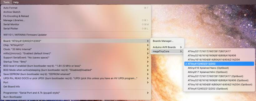
- This will update a bunch of things underneath Tools that you can already see in the image above. But be sure that Chip is set to ATtiny412 and the Clock to
20Mhz. - Within the Arduino Preferences click on the lowest link that goes to a
preferences.txtfile. This will open the folder containing that file.- Close Arduino app first and afterwards open the file (this is important, otherwise the
preferences.txtchanges will be overwritten). - Add a line to create a variable for the
build.path, which will contain all the build files that you’ll create through the Arduino IDE. For me, I addedbuild.path=/Users/nadieh/Documents/Arduino/build(TheArduinofolder was automatically created, but I created thebuildfolder within). - Open up the Arduino app again.
- Close Arduino app first and afterwards open the file (this is important, otherwise the
- I already had python3 and pyupdi so I could skip the middle section of the video and picked up again around 23 minutes.
I then saw Kris build up a similar pyupdi string to run. The first time it showed the exact same error when he ran the code. “YES!” I thought, “it wasn’t just me!” (^ᗨ^)
. Until he shows at 26m22s that he purposely hadn’t connecting his UPDI board to his LED board (the equivalent of my hexagonal board). After he connects the UPDI to the LED board and runs the command again, it all goes smoothly.
Henk also advised me to contact Quentin Bolsee to ask for help with the error. From him I learned that with the megaTinyCore add-on I could basically run all the steps within the Arduino IDE, not having to go back to the terminal and run the pyupdi command. He said: “try programming from Arduino IDE. There we use a better tool than pyupdi, and I patched it a few times to add the reset feature”.
There isn’t much in terms of “steps” to be found on the megaTinyCore website, except an almost hidden sentence that says “Choose Serial Port and 4.7k from the Tools -> Programmer menu, and select the Serial Port from the Tools -> Port menu”. Through my previous wanderings I had already set the port to my UPDI, and had selected that ATtiny412 as my board, so I only had to set the Serial Port and 4.7k. Within the Arduino IDE, I could then press the Upload button (the arrow to the right icon).
The process was working, and I could see information coming by in the terminal at the bottom of the screen. The results were sadly the same: UPDI initialisation failed
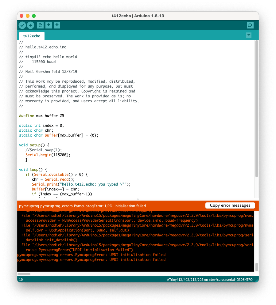
Ok, that convinced me that there just had to be something wrong with my board itself. I pulled out the multimeter at home and started checking the traces of my UPDI and hexagonal board, paying close attention to the UPDI lines. Although I had fully checked my hexagonal board already, I realized that I’d never truly checked my UPDI board, because I’d made it two weeks ago, when I didn’t yet fully understand continuity tests.
This time I discovered on my UPDI board that the continuity test from the UPDI connector made a loud beep still 2mm before it reaches the pin on the microcontroller, but stays silent when I touch the actual pin. Looking closer under a magnifying lamp and I thought I could see just the tiniest missing trace right before the pin indeed. Darn it! ヾ(*`⌒´*)ノ I guess I had taken away part of a trace with the hot vacuum pump two weeks ago. I hadn’t realized it yet because it was the UPDI pin, which I was only now testing for the first time.
Creating a New UPDI Board
The next time I was back in the lab, I pulled out the USB microscope and took a closer look at the traces of my microcontroller. And yes, now it was as clear as day that the traces were missing.
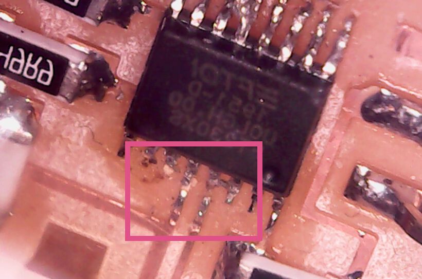
Henk helped me out and tried to create an “air bridge” from the traces to the microcontroller pins, but it sadly didn’t work out, and my UPDI was declared beyond repair. And thus I milled a new UPDI board.
I wasn’t looking forward to soldering yet another tiny FT230XS microcontroller though, but with enough soldering wick and patience I got it to work, without any problems along the way.
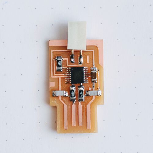
I was actually kind of happy to have a new UPDI board that didn’t have that ugly by-pass on it anymore (*≧▽≦)
Running the Echo Program
I connected my hexagonal board with the new UPDI and FTDI to try and get the echo program working on my board (I don’t actually remember at what point my blue LED started glowing, but I was super happy to see it!).
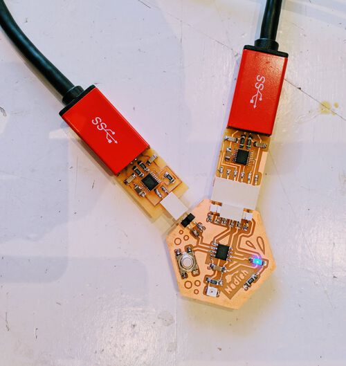
I set up the pyupdi command again, using the id of my new UPDI, and the new build folder where my .hex files were stored:
pyupdi -d tiny412 -b 57600 -c /dev/cu.usbserial-D30A3T7I -f ~/Documents/Arduino/build/t412echo.ino.hex -v
And it WORKED!! (ノ◕ヮ◕)ノ*:・゚✧
No UPDI Initialisation error statements, but a whole array of bytes being send, and at the end closing the UPDI port.

I could finally move on to the next step in Neil’s video, and that was to activate the echo program and start talking to my board, using the following command, which is using the FTDI serial number because the information is being transmitted through the FTDI:
# python3 -m serial.tools.miniterm /dev/your_device_port your_baud_rate
python3 -m serial.tools.miniterm /dev/cu.usbserial-D30A3T7C 115200
But of course this step didn’t go smoothly either, and I could type as much as I wanted, but I’d never get back the echo (╥_╥)

Debugging With the Logic Analyzer
At this point Henk pulled out his logic analyzer to see if the bits were being passed at all. He hooked up the GND and two more channels to the TX and the RX of my FTDI pins (I had to look up which pin was which from the KiCad schematic).
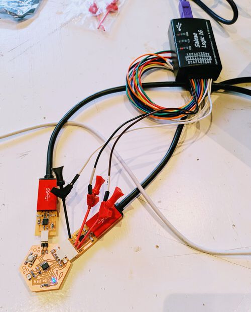
With the Logic Analyzer plugged into my Mac I opened up the Saleae Logic 2 app, which (after a little waiting) recognized the logic analyzer and that it had channel 0 and channel 1 connected, really handy! I didn’t have to do any other kind of set-up in there.
I would then run the miniterm statement from above. Within Saleae Logic 2 I would press the big green “play” button in the top right, quickly went back to my terminal, started typing some things, quickly go back to the Saleae Logic 2 app and pressed the giant “stop” button (if you don’t do this fast, the logic analyzer will have moved too far beyond the last time you typed, and it’s no longer saved).
I then scrolled along the history within the Saleae Logic 2 app, and saw a few “blips” in the channel 0! I zoomed in to one of the blips and could see a few up/down movements.
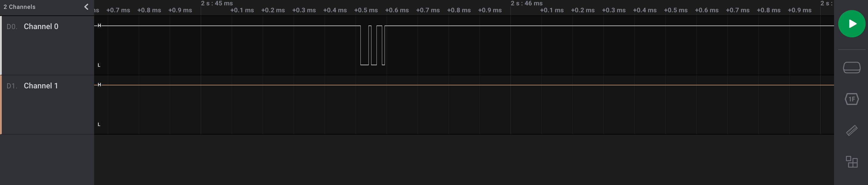
Checking the wires on my FTDI, I saw that channel 0 was connected to the TX pin. Ok, so the FTDI was sending along the data, but wasn’t receiving anything back.
I then hooked up the logic analyzer pins to my ATtiny412 to see if the data actually arrived at the pin of the ATtiny.
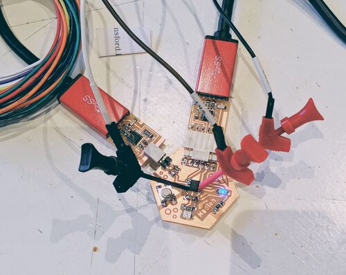
I redid the exact same process with running the miniterm command, typing while the logic analyzer was recording. The results were exactly the same, the channel 0 shows blips of bits coming in, but nothing was coming out of my ATtiny along channel 1.
Inspecting the Datasheet
Seeing that the bits were arriving at the ATtiny just fine, I wanted to inspect the datasheet and what it said about the TX and RX pins.
On page 15, chapter 5, I found a handy table that referenced which ports could have which types of functions
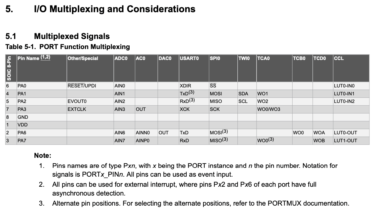
I compared this to the schematic we made with KiCad, and saw that we had hooked up TX and RX to pins PA2 and PA1, respectively. The table showed these two in reverse, but that has to do with the fact that the TX of the FTDI, the transmitter has to be connected to the receiver of the ATtiny. Vice versa, the transmitter of the ATtiny needs to be connected to the receiver of the FTDI, so that was all good.
However, PA1 and PA2 had a footnote next to them that read “Alternate pin positions. For selecting the alternate positions, refer to the PORTMUX documentation.". And when I looked closer, I saw that pin PA6 and PA7 are actually the default TX and RX pins!! We hadn’t connected our FTDI to the pins that the ATtiny expected to be the TX and RX!
I had NO idea what PORTMUX was. I went to that section in the datasheet, but it didn’t seem to give any information, just confusing tables…
Alternate Pins
I tried searching for answers online of course, about how to do PORTMUX in Arduino (I think it stands for port multiplexing?), and wasn’t able to find anything that was easy enough for me to understand, just a few answers that were beyond my knowledge.
Henk advised me to try and brute-force setting the RX and TX pins at the top of my echo script with
#define rxPin 1
#define txPin 2
but it didn’t make a difference. I tried swapping the 1 and 2, trying different kinds of numbers, but I would never get an echo back.
Eventually I asked Quentin for help again, and he replied to use Serial.swap(1); as referred to in this section of the megaTinyCore docs. I should really browse through that giant page of documentation when I run into issues the next time, haha.
Interestingly, that one line that is present in the echo example script online, but not in the video from Neil, which gave me compilation errors at the start (before I had installed megaTinyCore), was in fact the exact thing I needed to swap to the alternate TX and RX pins!
I put the Serial.swap(1); back into the void setup() function.
#define max_buffer 25

static int index = 0;
static char chr;
static char buffer[max_buffer] = {0};

void setup() {
   Serial.swap(1); //Swap pins, using the alternate TX and RX positions
   Serial.begin(115200);
}

void loop() {
   if (Serial.available() > 0) {
      chr = Serial.read();
      Serial.print("hello.t412.echo: you typed \"");
      buffer[index++] = chr;
      if (index == (max_buffer-1))
         index = 0;
      Serial.print(buffer);
      Serial.println("\"");
  }
}
I re-compiled and uploaded to my board via the UPDI, started the miniterm command again, and typed away:
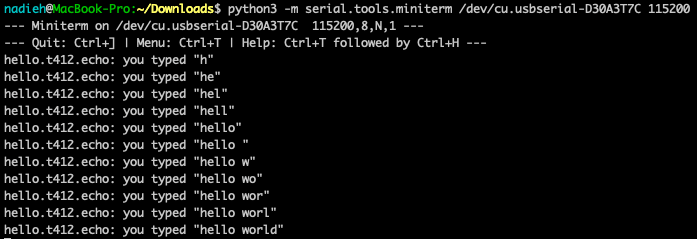
AND IT FINALLY RESPONDED!! (ノ◕ヮ◕)ノ*:・゚✧
Pfew! I finally managed to actually test my board and see that my UPDI, FTDI and hexagonal board were functioning and ready for week 8 in which I’d be programming the board to work with the button, LED and phototransistor.
Note | If the echo that you get back seems a not quite right (something is coming back but it looks odd), it can help to unplug the FTDI and UPDI from the USB cables and plug them in again for a reset; the PCB version of “have you tried turning it off and on again”. It can also be that you’ve used the wrong baud rate (I did some experiments to see what would happen, and with a different baud rate the echos back are some nonsensical marks).
Final Board
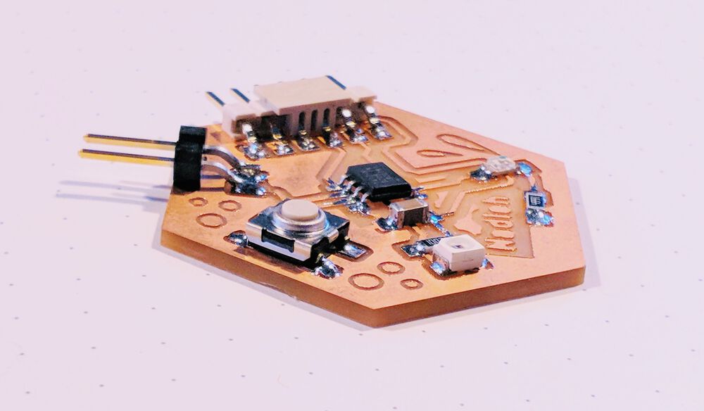
Reflections
The second part of the dive into electronics, lifting the curtain of how to create your own PCBs one more step.
What went wrong
I had to google a bunch of things about KiCad and I had to adjust my SVG files in Illustrator to make it work with mods, but those types of steps are so natural and expected that I don’t see it as something going wrong.
Part of me is still wondering if the footprints of the 1206 parts within the Fab Academy KiCad library are too far apart? When I checked the board of previous students, such as Tessel, the small resistors and capacitors seem to fit across their pads much better.
The main thing that went wrong was testing my board. Realizing that my UPDI board had a missing trace and had to be redone. And later realizing that we’d all created boards with the TX and RX pin connected to the alternate positions. Thankfully the fix turned out to be easy, although figuring this all out took quite some hours across several days.
What went well
I’m happy with the design of my board and what I learned from KiCad. I like how the result is not too standard, is clearly unique though, and I could apply some of the just-beyond-beginner aspects of PCB layout in KiCad, and that I haven’t made something overly complicated things just to be complicated (at least, that’s how I see it (•ω•) )
In general, the soldering went a lot better than the previous time, although I still cursed my shaky hands. I made sure to check if the first side I connected was truly fixed before trying to solder the other side. Quite a number of the FTDI and ATtiny pins had some nice flow action going on (but yes, the UPDI and button didn’t go quite as smooth, but should now be connected nevertheless). I don’t think this will ever be something I would ook forward too, but at least I wasn’t nervous anymore before starting as I had been two weeks ago.
And I’m really happy to have been able to test my board and see that it’s functioning, along with my new UPDI and FTDI boards.
What I would do differently
I’m not sure I really could’ve done this differently time-wise, but I would’ve liked to have had the time to design my PCB with one or two other tools as well. LibrePCB and EasyEDA seem like good alternate options (or even Tinkercad). But also the pcb.py package (with the updated frep_gpu.py file) to create a board with scripting seemed interesting. Although, having now experienced how much fiddling and moving things around while in KiCad’s PCB layout editor, I think that doing it via a GUI is much easier in this case.
Nevertheless, I’m glad I took the time to dive a little deeper into KiCad instead and learned about copper pouring, non-standard angles, cleaning up labels, adding text and graphics, the margin and drawings layers, power flags and so on.
I didn’t get around to try and simulate the design either. I looked at a short video about doing a simulation within KiCad, but when I checked the Spice model of the components while in the Schematic Editor Layout (hover over a component, press E and click Edit Spice Model…) I saw that most were not set-up for it, apart from the resistors and capacitor (the ATtiny and button were somehow set-up as a resistor?). And figuring out how to make spice models for all these components, when I didn’t even fully understand them seemed like a giant bridge too far for this week.
I did eventually see that you could do simulations with Tinkercad much more easily than the gist I got from KiCad, see this video for example. But by that time the week was over and I had to focus on designing something big instead. If I have to simulate anything in the future I would want to take a closer look at Tinkercad’s options I think.
Wrapping up
I quite enjoyed taking one plunge deeper into the realm of electronic design and learning how to create a schematic and layout a PCB. I learned more about the general components that go onto a board, but I would definitely not feel confident enough in my knowledge to figure out how to create a PCB from scratch and know what components are needed in what kind of connection to, for example, make a LED light up on a button press. So I’m looking forward to learning that (and programming the board in general) in upcoming electronics weeks!