We’re learning how to fabricate our own PCBs (printed circuit board) this week. Creating the board with a very precise milling machine and learning how to solder teeny-tiny components on top of it. I’ve never soldered anything in my life before, and I have shaky hands, so this should be… interesting (ʘ‿ʘ)
Assignments
Our tasks for this week are:
- Group assignment: characterize the design rules for your PCB production process
- Individual assignment: make an in-circuit programmer by milling and stuffing the PCB, test it, then optionally try other PCB processes
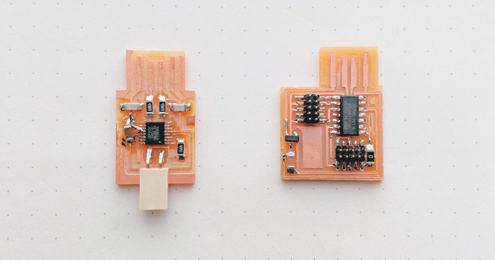
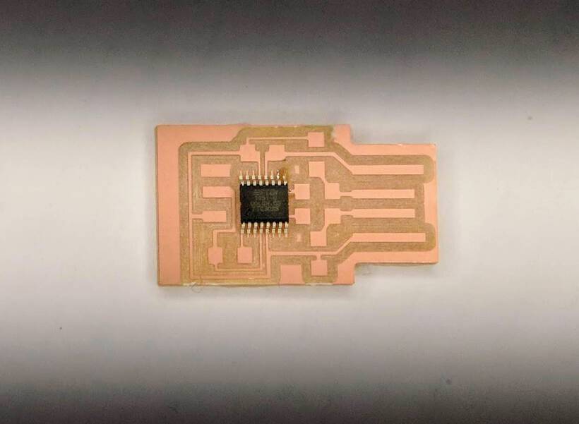
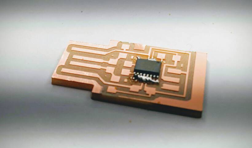
Hero Shots
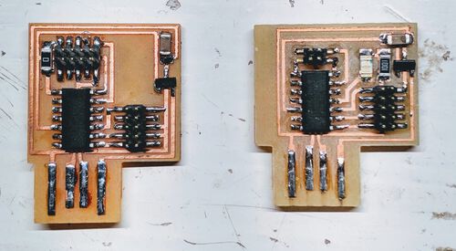
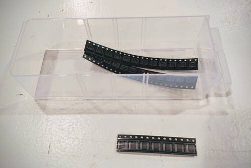
Although they won’t win any beauty prices, here are the final results of the two boards I created for the tl;dr to hopefully show you why the rest of this very long blog could be interesting to read (⌐■_■)

A Little Info on Boards
This week is so utterly knew to me, please forgive me if I explain some electronics part wrong in the section below.
We’re going to be fabrication our own PCB. However, we’re not really getting an explanation about what a PCB does, nor why you should use one model/type versus the other. I’ll try and describe what I wrote down during a quick intro into at the lab about the different boards.
- ISP | In System Programmer | There was a “Fab ISP” board whose heart is the ATtiny45. We’re not going to be making or using this, I believe because it works with older ATtiny models.
- UPDI | Unified Program and Debug Interface | You can recognize it by having two lines (in the white rectangle). This is used to communicate with the microcontroller on the board (to input/output the results of the calculations done by the microcontroller), talking to it in serial. It combines the TX (transmit) and RX (receive) info into one of its two legs/lines, while the other is the ground.
- FTDI | Future Technology Devices International Limited (I think…) | You can recognize it by having six pins. An FTDI does serial communication through a USB port, and has a separate port for the TX and for the RX. You can’t program a new board with an FTDI, you only use it for communicating from USB to serial.

- JTAG | Joint (European) Test Access Group | These are used to program SAMD microcontroller chips I think.
The black rectangular boxes with many legs in the heart of each board are the microcontrollers, which are integrated circuits, meaning that all the components are hidden inside. They are designed to perform a predefined task (you give input, the controller gives an output) that you program it to do. It has no working memory so you can’t store anything on it, and there’s no operating system on it. During the Fab Academy I believe we can have access to two different brands of microcontrollers:
- ATtiny | Created by Atmel (part of Microchip since 2016?) | It has an 8-bit processor.
- SAMD | Created by Microchip | It has an 32-bit processor and is bit newer than the ATtiny. You program these with a JTAG.
UPDI, ISP, and JTAG are different protocols to program your microcontroller with. They are not interchangeable.
The PCB Milling Machine
Our Fab Lab has a Roland Modela MDX-20 for milling PCBs. It has a precision of 0.006mm!
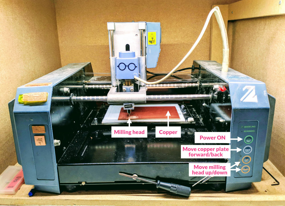
Press the top green button to turn the machine on. This will make the head of machine go to its origin, the top-right corner. The grey VIEW button will put the plate into (or out of) “view” mode. In case the plate is already in the front, pressing this will make the plate move towards the back, ready for alignment and eventual milling. If the plate is in the back, pressing VIEW will move the plage forward, so you can get to the plates.
The Plates
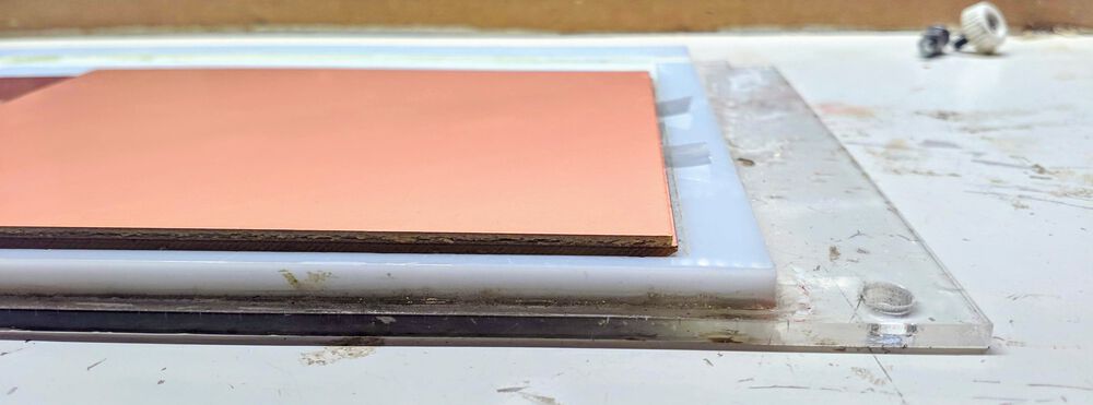
On the bed of the machine lies a plate with several layers. From bottom to top:
- At the bottom there is the the default glass plate that comes with the machine. You don’t want to mill into this plate.
- On top of that, our instructor Henk has glued a white acrylic plate. Into this plate he milled out a depression. This makes the floor of the white depression perfectly level with the machine. You also don’t want to mill into this plate.
- Next there is a sacrificial (copper) plate. This serves as a protection between the copper plate out of which the PCBs are milled and the acrylic white plate. When milling out the outline of a PCB, the milling machine can/might mill a little bit of this sacrificial plate as well, and that’s fine. However, after this plate has had too many scratches, it needs to be replaced.
- On top is the final copper plate out of which the PCBs are milled.

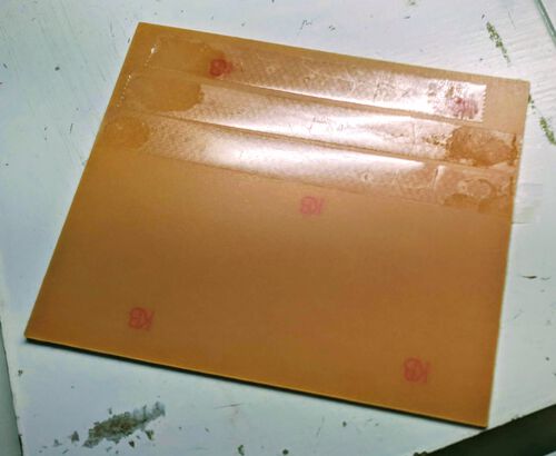
The copper plates used are FR-1 boards that consists of a thin layer of copper over a non-conductive phenolic resin. The copper is milled away which leaves traces to which electronic components can be soldered. There are also FR-4 boards, however these are not used for milling, because the lower part is made of glass epoxy. The glass dust that comes from this is really bad for your health when it comes into your eyes, mouth or lungs (and I would expect that it’s not good for the longevity of the tiny milling bits either).
All four layers are stuck together with double sided tape. When applying a new upper (or sacrificial) copper plate on top, it’s important to remove any remaining residue of the double sided tape still there. Clean the sides with some tape removal liquid. Next, apply a new layer of double sided tape to the full underside of the plate. The reason to put tape on the whole underside is to make sure that your small PCB will remain in place when the interior is milled out, no matter where on the board this happens. Make sure not to overlap the tape. Otherwise, you will create a bump there.
With the new copper plate in place, put the whole base back into the machine, using two screws at the front to fix it. Tighten the screws, but only just (the next person should be able to unscrew them again).
The Milling Bits
The lab uses the following sizes (in diameter):
- The 0.4mm bit is used to mill the traces of the board. It’s really tiny and very breakable.
- The 0.8mm bit is used to mill the outline out of the board. Because it’s bigger it can go a lot faster than the 0.4mm bit. It’s still easily breakable.
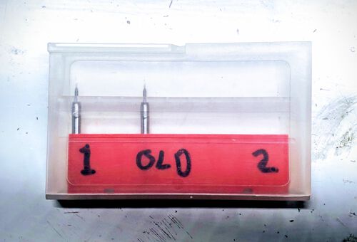
The 0.4mm bits come in both a single and double flute, this refers to the number of blades on the milling bit. You can see the difference in the image below right, the double flute is the left bit.

Note the length of the tiny top part of the milling bit. These are not meant to grind down with extended use. If you do see that your bit’s top is shorter than normal, that means that it has broken and you need to replace it.
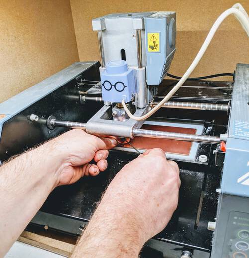
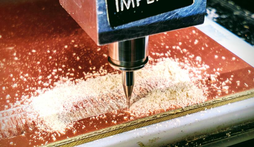
Operating the Milling Machine
Milling a PCB happens in two milling steps. First you mill the fine traces from the top and next the interior is milled out of the copper plate.
Put the machine in the non-view mode, where the plate is moved to the back.
Changing Milling Bits
The milling bit is held in place by two grub screws. Slowly unscrew the grub screw that is marked in green (to make sure only one side is ever used to (un)screw) to release the milling bit. Use the small Allen key that is generally held to a magnet at the front of the machine. Be sure to hold your finger against the milling bit while you unscrew! You don’t want the bit to to fall and break.

Now gently move the milling bit out of the head and place it back where it belongs (the 0.8mm bit is generally placed against one of the magnets at the front of the machine and the 0.4mm bit goes back into a box). Grab the milling bit you need and place it into the head, again holding your finger against the bit for some pressure so it won’t suddenly fall. Move the milling bit a little up (but not too far, the image below shows a good position as to how far up it should be). Tighten the screw a little. You’ll need to do the fine-tuning of the z-axis later.
Mods PCB Program
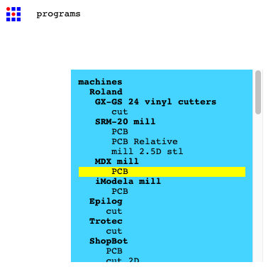
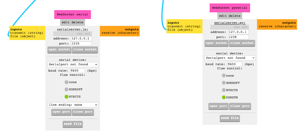
If the computer attached to the machine has just turned on, you need to start mods first. Open a terminal and type mods. Next open the web interface of mods (at 127.0.0.1:8080). Right-click anywhere and choose programs from the window that appears. Next, choose open program and then choose MDX mill -> PCB
A web of connected modules opens on the screen. Along the far left side you can load either an svg or png for the traces or interior structure to mill. Because of the precision required you can’t use jpg as an image format.
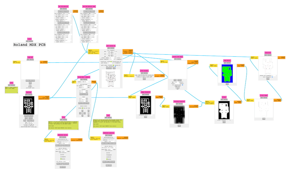
The way the computer is connected to the machine means that we need to use the serialserver.js as a connection. Therefore, first make sure to press close socket and then close port on the WebSocket pyserial module, and open socket and then open port on the WebSocket serial module, which are located in the middle bottom of the module web.
Load the svg or png of the traces of the PCB. It’s the black area of the image that the mods program will use to create its paths to mill away. In the set PCB defaults (mm) module, click on the mill traces (1/64") button.
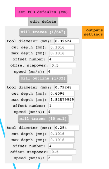
This will copy over the default settings of a 1/64" milling bit to the mill raster 2D module, located to the lower-right. However, Henk told us that these 1/64" default settings aren’t quite correct for our machine, some need to be adjusted. To explain what they mean:
- Tool diameter: 0.3962mm is close enough to the 0.4mm so leave be
- Cut depth: Change from 0.004" to 0.003"
- Max depth: Change from 0.004" to 0.003"
- Offset number: The number of times the drill bit will go around and carve away the copper. The default of 4 is good (usually)

- Offset stepover: What fraction of the previous path shall the bit overlap in tracing out the next path. The default of 0.5 is good
- Direction: Keep to climb
- Path merge: We couldn’t figure out what this does
- Path order: In which direction will the calculated path be cut out. Basically always forward

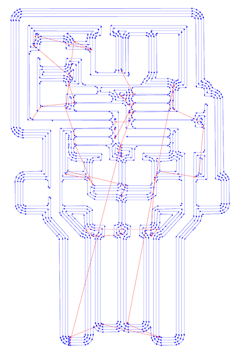
When you’ve updated these settings, press calculate and mods will calculate the path to trace. When it’s done calculating, a new window opens in which the calculated path is shown (blue will be milled away, red are the path-up movements).
Next, in the Roland MDX module (to the lower-left of the mill raster 2D module) set the model to MDX-20 and for the 0.4mm bit, set the cut speed to 1mm/s.
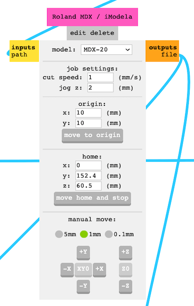
Setting the Origin
Next we need to set the correct origin of the drilling bit with(in) the Roland MDX module. You want to position the head at a place above the copper plate. The origin represents the bottom left corner of your PCB board’s loaded image. Change the numbers in the origin section and press move to origin to make the milling head move there.
When you feel that the head is almost right, move the drilling head down somewhat to better assess it’s position above the copper plate. Move the head down with the UP/DOWN buttons on the machine itself, not the +Z/-Z buttons in mods! Just leave the whole manual move section alone. Just to note, it will take a little while before the head actually moves after pressing the UP/DOWN buttons.
Adjust the origin further if you need to. Write down the final origin x and y coordinates you’ve set.
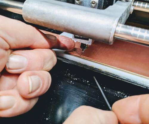
Z-aligning the Milling Bit
With the origin fixed we need to properly z-align the milling bit. With the DOWN button, move the milling head all the way down. Then, move it just a pinch upward, about 2-3mm, but make sure that it’s moved upward higher than the thickness of the plate you’re milling (the copper plate we’re using is about 1.5mm). This will make sure that the milling bit can move low enough to mill out the PCB from the plate.
Hold your finger against the milling bit again, so it won’t drop down, and slightly unscrew the (green) grub screw until you can move the bit.
Now gently move the bit down so it’s pressed against the copper plate. Keep a little pressure downward on the finger with which you’ve been “holding” the bit, so it’s kept snug with the copper plate during the next steps: Lightly move the round cylinder that holds the grub screws back and forth to make sure that no dust or particles are stuck within it and then tighten the grub screw again. The milling bit is now z-aligned.
Milling the Traces
Back in mods, press calculate again, just to be sure. Go to the WebSocket serial module and press send file to start the milling process of the traces.
If you want to pause the process to check for example if the traces are being cut out deep enough, you can press VIEW at any point during the milling. This will pause the process and make the copper plate move forward. If all looks good you can resume the process by pressing the VIEW button again.
If something goes wrong, you can cancel the milling job: Press cancel in the WebSocket serial in mods, then press the VIEW button and then gently press the UP and DOWN button at the same time for 10 seconds. After 10 seconds the green light (top-left of the 4 buttons on the machine) will blink. This will flush the memory of the machine so you can reset your job with mods.
When the machine finishes it will automatically move the plate forward. Grab the handheld vacuum cleaner (hangs to the left of the machine) and clean the dust away from the PCB to check your traces.

If it all looks good it’s time to mill the interior out of the copper plate.
Milling the Interior
Switch the milling bit from the 0.4mm to the 0.8mm, see the instructions for changing bits in the “Changing Milling Bits” section.
Press VIEW again to move the plate back into the machine (I think I need to press VIEW twice actually. The first time the milling head moves to the origin, the second time the plate moves back and the milling head moves to the last-set origin).
Within mods load the interior png (or svg) file. This time select the mill outline (1/32") default from the set PCB defaults (mm) module. The tool diameter of 0.7924mm is good, the default cut depth of 0.6096mm as well, however change the max depth from 1.8287 mm to 1.55mm (this number is something Henk learned through experience). Press calculate to see the resulting path.
This time, the calculated path will not lie in a flat plane, but go into the z-direction as well. You can see this by pressing view in the view toolpath module (towards the right of the mill raster 2D module) and rotating the path (right-click and drag).

Within the Roland MDX module, change the speed to 4 and make sure that your origin is still correct. Press move to origin in case the drilling head isn’t there already.
Now z-align the milling bit again, see the instructions in the see the “Z-aligning the Milling Bit” section.
With everything prepared, press calculate again, just to be sure, and when it’s done, go to the WebSocket serial module and press send file to start the milling.
This time the milling will go quite fast, only taking two or three minutes.
Removing the PCB
When the machine is done, has moved the plate forward, and you’ve vacuumed the dust away again you need to check if the PCB is been completely milled out of the copper plate. Take the screwdriver that’s generally attached to one of the magnets on the front of the machine and gently wiggle it along a side and try to flip it upward to see if it comes loose. Due to the double sided tape on the back of the copper plate / PCB it can seem as if it’s still stuck to the copper plate. Be gentle and assess which situation you’re in.
After taking the PCB from the plate remove the double sided tape from the back. In case you have burrs on your PCB you can sand the PCB with paper.

You can clean the PCB with some soap and water and now you have a milled PCB!
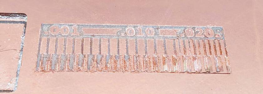
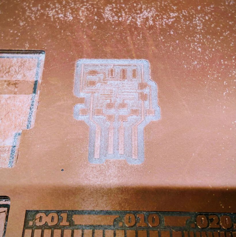
Milling Precision Test
For our group assignment we had to mill a test that would show the precision of our milling machine. Both in terms of how thin of a line it can mill (with ample space along the sides to mill away), before it becomes so thin that it gets lifted off the yellow epoxy backing. And what the thinnest line is that it can mill between two close traces, giving you basically the diameter of the milling bit.
From the Fab Academy page for this week you can download the test traces and interior png files (the last entry in the CAM section).


We loaded the traces png into mods and changed the settings for the 0.4mm milling bit. And that’s about all we did right at the start..
Here is a long list of the many things we did wrong, written in how you should be doing things (I’ve also mentioned many of these in the instructions section above):
- Align the z-axis on the top copper plate, not the sacrificial plate (i.e. the “bottom” of the top copper plate)
- Perform the z-axis aligning after fixing the origin. You can’t assume the z-axis is exactly the same if you move the origin after having done a z-alignment.
- Don’t use the manual move buttons within mods to move the milling head, especially the +Z/-Z buttons. This will move the milling head, however, it will have no effect on the z-alignment of the milling head. We hadn’t realized how long it takes before the milling head will actually move up or down when pressing the UP/DOWN buttons on the machine. We thought something wasn’t going right there and therefore used the +Z/-Z buttons within mods, since the previous week we’d seen that we can also move the laser cutter with software. We were quite surprised to see the milling head move upward when we pressed send file and it starting milling the air!
- Extra lesson learned: Don’t assume that the way things work on one machine translate to how they work on another machine.
- Don’t push the milling bit too far up into the milling head when you first put it in (before the z-aligning), otherwise you have almost nothing to grab onto when you want to move it down again.
- Be sure to only (un)screw the green-marked grub screw when releasing and tightening the milling bit in place. We got ourselves in a weird situation with the grub screws. Somehow, after many mistakes already made, the screw had been (un)screwed often, and suddenly it seemed as if a screw was missing on one side. Henk therefore placed another one in there. However, the milling bit was also completely stuck in the milling head. Henk too out the entire milling head and inspected it, eventually realizing that we hadn’t lost the grub screw, but had screwed it in so far that it seemed lost. Furthermore, this grub screw was completely blocking the milling bit from being able to move down.
- Have just a little downward pressure on the milling bit as you wiggle the grub screw part and tightening the grub screw again. Otherwise chances are that the milling bit has moved upward just a little, which is enough to not fully cut out the traces, ruining your milling run. Due to the dust produced, you’ll really only see this after the milling process is finished and you’ve vacuumed the dust away ಥ﹏ಥ
Due to all these mistakes, all four people in our group were working with mods or with the machine at different stages, and everybody basically had a hand in making a different mistake. Mine was to not push the milling bit a little down when z-aligning it ruining our first milling run ( ╥﹏╥) ノシ
We’d had a particularly difficult time with everything relating the the z-axis of our machine in essence.

Thankfully, after z-aligning the milling bit again (with a little downward pressure) our next run was finally a success!
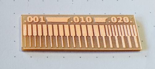
The bottom row shows how thin a line can get, and even the thinnest line of 0.001" looks perfect. In millimeters this is 0.025mm, and since Henk told us that our machine has a precision of 0.006mm that was to be expected. The top strip shows that mods didn’t add any path traces into any strip smaller than 0.016", which is 0.41mm, thus having proven the diameter of our 0.4mm milling bit.
Milling My Own PCB
Having finished the test it was time for each of us to mill a board. Henk wanted us to make a UPDI, the hello.USB-UPDI.FT230X specifically. I downloaded the traces and interior png files from the Fab Academy’s long list of programmers.

I set-up the milling machine and mods (following the steps I wrote in the “Operating the Milling Machine” section). However, I made one small change. Fellow student Erwin had gone before me and he noted that there was just a little too much copper left along the bottom side (where the PCB is less wide). It wasn’t really an actual issue, because he could scrape that excess copper off (with a screwdriver?). I wanted to see if I could fix that with the machine itself and therefore set the offset number from the default 4 to 5, meaning the machine would do one more pass along the outside (and inside wherever there was enough room). Hopefully that would have fully milled out the copper along the edge of the bottom side.
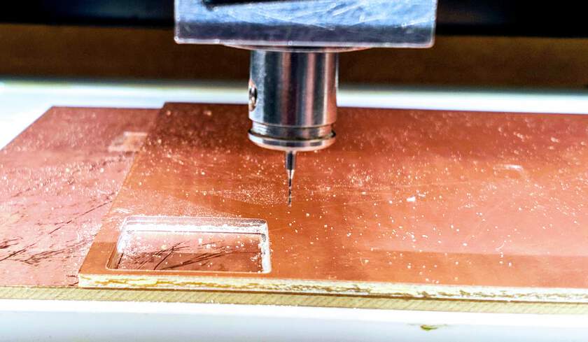
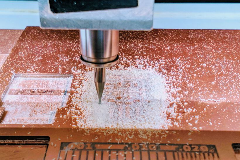
Below are some “action shots” of the milling process:
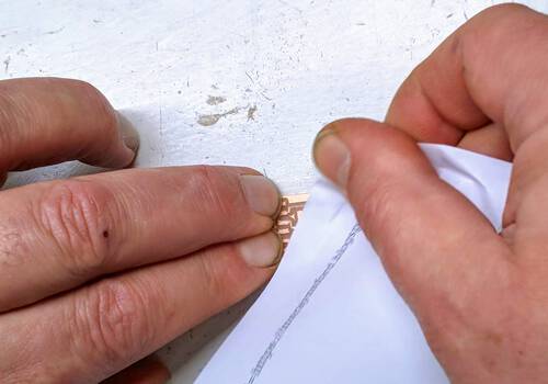
After the interior trace was done as well, I vacuumed the dust away, and carefully peeled it out of the copper plate with the screwdriver. I then removed the double sided tape from the back and used some soap and water for cleaning.
There was just the tiniest but if copper left along the bottom edge, however I could peel it off with my nail.
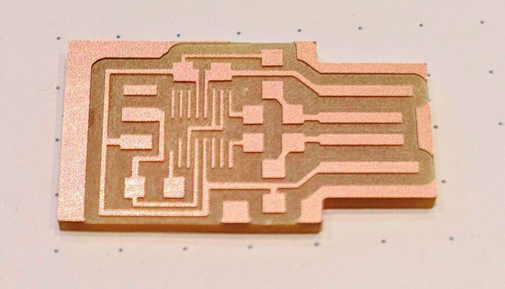
The milling of my UPDI looked like it had succeeded.
Soldering
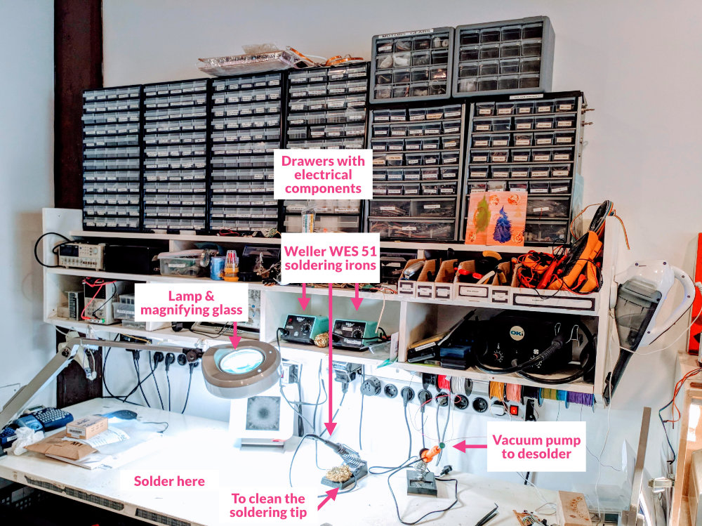
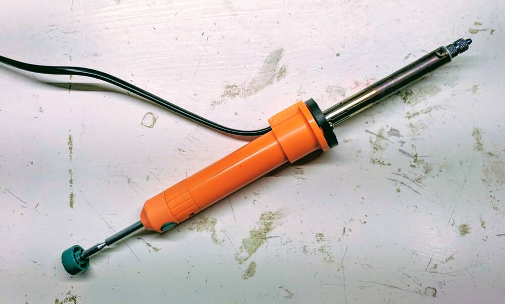
With the board milled out, you have to solder the components onto it. At the Waag lab there are several different types of soldering irons:
- Two Weller WES51 | American brand, quite expensive.
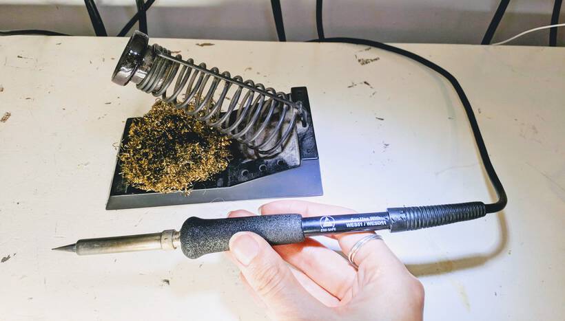
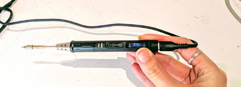
- A TS100 and a TS80 | Chinese brand and very affordable. The TS80 can be charged with USB-C and heats up to 300 C° in a matter of seconds. You can set the temperature with the little buttons and screen on the iron itself.
Preparing for Soldering
- Start by degreasing your board with plain soap. Rub it well, wash it all off and make sure to dry it really well (electronics don’t go well with being wet).
- It’s much easier to solder if the board isn’t moving as you’re working with it. An easy way to fix the board in place is by applying some double sided tape on the paper and sticking the board to it (you can of course still rotate the paper to work on different parts of the board).
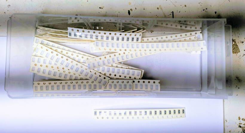
- When gathering the components that need to be soldered onto the board, take one component at a time from the little drawers and place it back before taking another tiny drawer with the next components. Otherwise you’re bound to mix components up. And furthermore, you’ll forget exactly where to place the little drawers back.
- Get a good tweezers where the tips come together.

- Get the solder (fyi: the one in the lab still has lead).
- Get your soldering iron ready in the soldering station and heat it up.
- Grab some soldering wick to remove excess solder.
- Also heat up the vacuum pump that is used to desolder. It’s handy to use a vacuum where the tip also gets hot. This way you only need one tool to both heat up the solder and then suck it away.
- It would be good to know where the hot air gun is located, in case you need it to desolder a component from your board (when a mistake is made). This gun will blow hot air that makes the solder melt so you can pluck out the wrong component.
- A general technique is to hold up the board by the component that you want to remove, blow the hot air gun at the places where the component is connected to the board, and let gravity do its work, letting the board fall when the solder has heated up enough to melt.
- A hot air gun can also be used for soldering itself when using soldering paste. In this case the hot air gun will make the paste melt and fixes the components to the board. However, we’ve not used this technique.

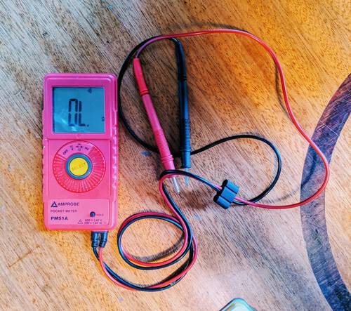
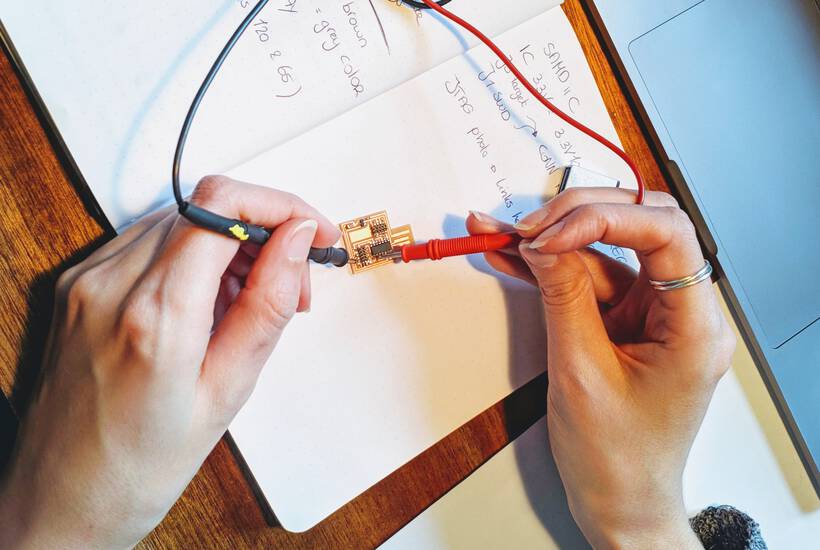
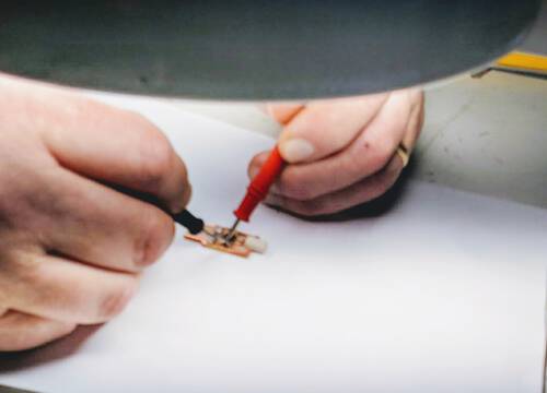
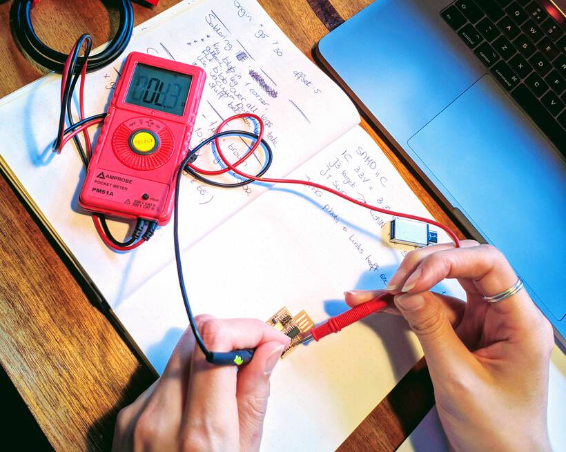
- It’s also handy to have a multimeter with which you can check if lines/traces still exists, that the correct parts of the board are in contact, and that parts that shouldn’t be in contact aren’t.
- You touch one of the two tiny tips of the multimeter to one trace/pin/leg and the other one to some other trace/pin/leg and depending on what you’re testing, you hope to hear or not hear a beep. A beep occurs when the two things that you’re touching are connected (you’re creating a short-circuit in that case), and it will stay silent if the two points that you’re touching are not connected.
- Bonus tips: No coffee at all (no problem for me, I’ve never had a cup of coffee in my life), and a good night sleep beforehand.
Soldering Tips
When you’re ready to solder, keep in mind to go from small to big components, work from the center outward, work from the low to the high components. I know these rules can contradict each other so you’ll have to figure out the most optimal order.
First, clean the tip into a wet sponge or with a good rub against the brass. The tip needs to look shiny. Next, add a tiny bit of solder to smoothen out the soldering tip.
Although many components can be soldered in both ways, there are components that need to be placed in a certain direction. Microcontrollers for example have a certain polarity. Look at a close-up photo of the board you’re copying to see in what direction the components should be fixed. And if that is of no help, you can (apparently) find the info in the data sheet of the component. For some microcontrollers you can recognize the direction by a tiny indented (or white) dot in one corner.
The steps for soldering components that are connected with two pads:
- Touch the soldering iron tip to one pad and heat it up.
- Add just a bit of solder and let it flow to create a small bump of solder on the pad.
- Using the tweezers (in your non-dominant hand) place the component where you want it, with one side on the pad you just added some solder to, and keep it in place.
- Move the soldering tip back to that pad and heat both the component and pad to make the solder connect the two. Don’t add more solder at this point.
- Afterwards test if the component if actually fixed well enough in place by gently touching it with your tweezers to see if it moves. If yes, put it back in place and add a bit more solder.
This has fixed one side, and you can properly solder the other side.
- Heat the other side, both the pad and the component.
- Touch a little solder on it (don’t shove it in), and let it flow.
- Remove the solder.
- Then remove the soldering tip.
- Go back to the other side and this time solder it properly: heat both the pad and component, add a bit of solder and let it flow, remove the solder, and finally remove the soldering tip.
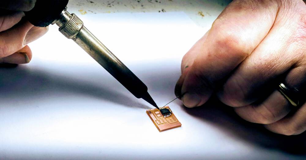
When you solder a component that has many legs that are too tiny to solder separately, such as (some) microcontrollers, there are several differences in the steps:
- Touch the soldering iron tip to one of the four outer tiny traces and heat it up.
- Add just a touch of solder and let it flow.
- Use the tweezers place the component and hold it in place.
- Move the soldering tip back to the trace with the solder and heat both the leg of the component that lies on that trace and the trace itself to make the solder connect the two. Don’t add more solder at this point.
- Now we’ll fix the cross side as well (e.g. if you did the top-right leg first, now do the bottom-left leg). Heat the trace and leg of the component, add a bit of solder and let if flow. Remove the solder, and remove the tip.
This has fixed the component, and you can properly solder along all legs.
- Heat up all the legs along one side.
- Add a big blob of solder across all the legs of the heated side.
- Using the vacuum pump, slowly start sucking away the excess solder:
- Push the pin on the back into the pump.
- While keeping your hand along the back of the pump, so you can have a finger on the pump’s release button, touch the (hot) tip of the vacuum pump to the blob.
- When the solder melts, press the button on the vacuum pump to make it release and suck away the solder.
- The solder only wants to stick to the copper, not the yellow epoxy layer, so it’s the solder that’s on top of the yellow layer that gets sucked away.
- Repeat the vacuum pump steps until you’ve sucked away all the excess solder and all the legs are clearly separated, from the top till the traces.
- However, you can also use a soldering wick to remove the excess solder. Place thee wick on top of the solder and then the soldering iron tip on top of that. It then takes some practice and feeling, but if done right, the excess solder will flow into the wick.
For components with more than 2 legs, but still big enough or far enough apart to solder each separately, follow the first steps from the multi-leg explanation above. Where you first solder one corner, and then the opposite corner to fix the component in place. Next, follow the steps from the two-pad steps to properly solder each leg, finishing off with properly soldering the two legs you did first (which were mostly keeping the component in place till then).
Checking the Soldering
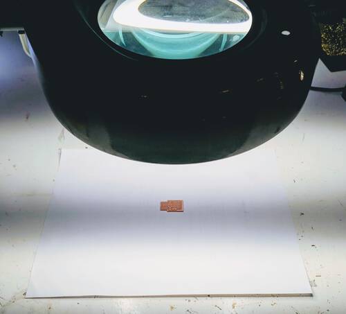
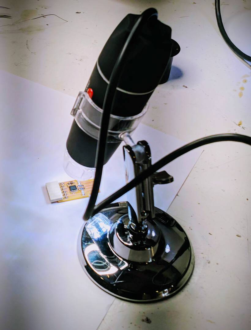
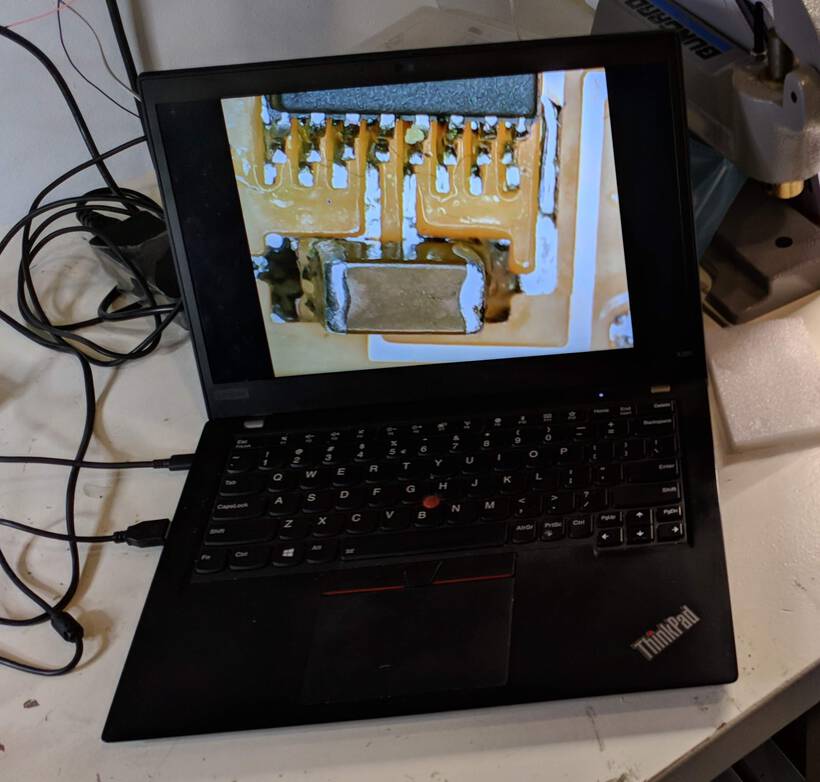
You can use a magnifying glass to check how well the soldering went, and if no two traces have unintentionally been connected. If you can’t see it well enough with a magnifying glass, use a USB microscope.
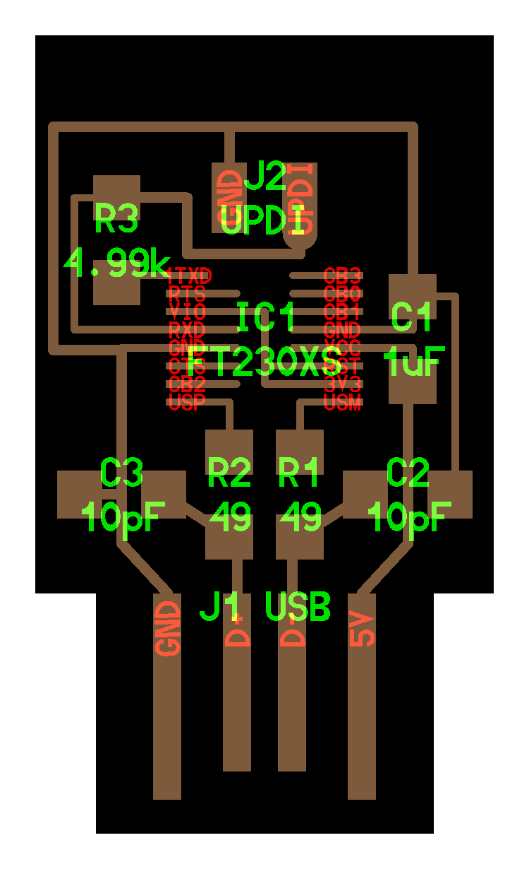
Soldering My UPDI
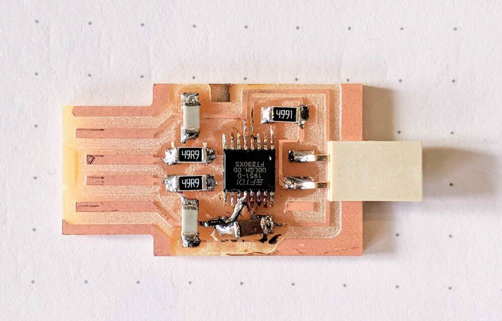
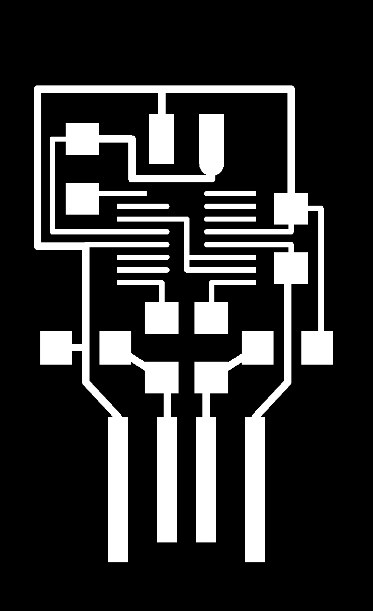
With my hello.USB-UPDI.FT230X milled out, I could solder the components onto it. From the Fab Academy site with all the info about the possible programmers, you can find a schematic overview of the components, plus a photo of the final result to help you in the process.
Some of the photos in this section are not sharp, which I only realized later when I was processing them. The items and work that we’re doing with the soldering is just so tiny that my phone camera just can’t focus well enough sadly.
Gathering the Components
Using the schematic, I gathered the following components:
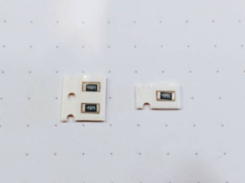
- Resistors: These thankfully have their Ω printed on the front, so you know later on which resistor it is
- R1 & R2: Two resistors of 49 Ω
- R3: One resistor of 4.99k Ω
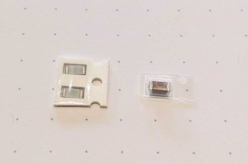
- Capacitors: These sadly have no text, but seem to be color coded instead
- C1: One capacitor of 1μF (micro Farad), which has a brown color
- C2 & C3: Two capacitors of 10 pF, which have grey colors
- IC1: One FT230XS microcontroller (Integrated Circuit), which apparently is an FTDI chip. This now makes me confused, because I thought the UPDI and FTDI were different… ⊙︿⊙
- J2 UPDI: The white box with two pins from the photo above. I was unable to find this in the component wall, until Henk pointed it out: it’s called Conn SMT 2WAY. From what I understand there’s sadly no universal way to name each type of component (I guess there are just too many). Henk explained that it’s called 2W, 2.54MM PTH SOCKET, SIL, SMT in the Fab Lab Inventory, and it’s Digi-Key component name is BG300-02-A-L-A, both of which are not very descriptive names. Henk therefore chose to name it Conn SMT 2WAY, as it’s part of the Connectors, SMT (or SMD, for surface mount) and 2way (2W-2legs/female).
Soldering the Components
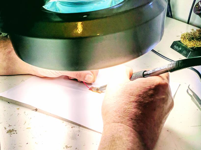
I had looked at a few “soldering intro” youtube videos as preparation during the previous evening and the morning commute and was truly a little nervous when sitting down and starting.
With the “small to big, the center outward, low to the high” rule in mind, plus this being the very first time I would ever solder anything, I decided to start with the central R1 and R2 resistors. They have big pads that would make it easier to heat up both the pad and component, while having space to add in the solder.

That thankfully went easy and smooth, although I wasn’t sure if I’d added too little solder. While holding the component in place with the tweezers and then adding the soldering iron to heat up the pad with solder to fix the component in place I realized: You really want to hold both the iron and tweezers in your good hand since it’s such precision work (*^▽^*)ゞ Not possible of course. I experimented a little and found that holding the iron in your good hand is the better choice.
Next up was (theoretically) the most difficult component to add, the microcontroller chip in the center. With the legs and traces much to thin to solder each separately, I followed the steps I outlined in the Soldering Tips section above. I addded just a little solder to the left-top trace to slightly fix the chip in place, after which I added a royal blob of solder to the other side.
I believe that using quite a lit of solder in this case is a good thing, because it makes it easier to melt it again with the vacuum pump and suck it away. Although I was thankfully successful in sucking away the excess solder from all the legs of my chip, it really wasn’t an easy process. The nozzle of the vacuum pump, although small, just felt huge in comparison with the tiny legs of the cip, and it was very hard to place the nozzle in a way that it makes contact with the solder enough to heat it up.
I also tried getting rid of some solder by using solder wick (a little braided wire of solder that you place onto the solder and heat up, when the solder melts, it should be wicked into the wire), but I wasn’t having any success with that. Perhaps I was just using the wrong technique, because it did seem promising, since you can place it onto the legs of the hip mich easier and use the fine tip of the iron for precision heating.
Nevertheless, I eventually had my chip soldered onto the board with seemingly all legs disconnected.
And Then It Went Wrong
I thought the worst was behind me and started soldering the bigger 1μF capacitor. However, while soldering the 2nd side I had apparently not fixed it well enough on the 1st side, because my hand suddenly made a little more violent shake than normal and I just shoved the whole capacitor across the board, dragging solder along. It was of course fixed to the board utterly wrong within a second.
That’s a mistake that can happen. However, I then made the big mistake. I tried to remove the capacitor with my soldering iron. By heating up the solder with the iron and then pulling it upward. The downside is that you an only heat one tiny section at a time, so it was quite hard to slowly get it away from the board. And when I finally pulled it loose, I also pulled away a tiny trace running from the chip (⑉⊙ȏ⊙) (and also almost one of the pads).
In retrospect, I should’ve/could’ve used the hot air gun to desolder my capacitor from the board. Although not without its faults and ways in which it can go wrong (you can possibly also heat up other components that get scattered when the plate falls away with gravity from the one component you’re trying to desolder), I think it would’ve been the better tactic here.
I wasn’t 100% sure that the trace was gone at this point, it was a little hard to see. Henk was busy, so I just decided to hope for the best and soldered the remaining components onto the board, which thankfully went smooth (I also made sure to check if each side was actually fixed, before soldering the 2nd side).

PCBs Can Also Get a Bypass
With all the components on my board, but with the fear that one trace was gone, I asked Henk to check my result. He used a multi-meter to check the connections, and indeed, that one trace was completely gone sadly.
However, it seemed I was partially in luck, because Henk said that we could add a “bypass” from the chip’s 4th leg (counted from the bottom, the one that says VCC), to the line behind the 1μF capacitor.
This involved cutting a piece of (quite thick!) wire into a tiny, tiny section, bended very specifically, and trying to solder it exactly at the right place: touching only the 4th leg of the cip, and then against the bottom side of the capacitor. I tried doing this for a bit, but I really didn’t have the skill/experience, plus quite shaky hands. Thankfully, Henk came to the rescue and made the bypass after some fiddling around ʕっ•ᴥ•ʔっ
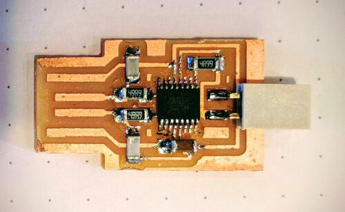
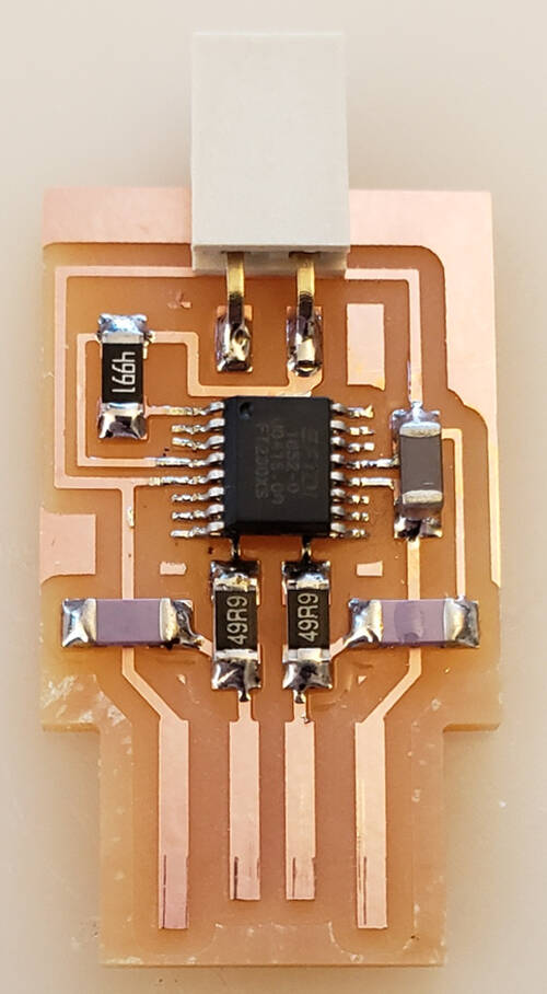
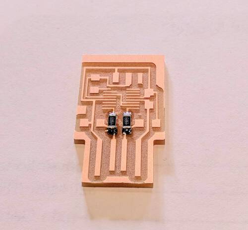
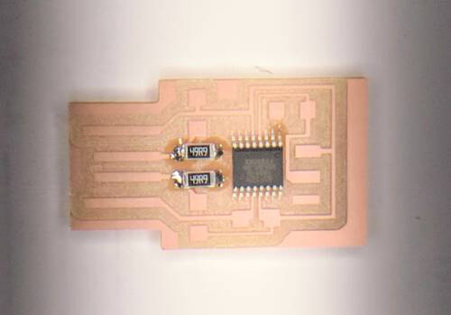
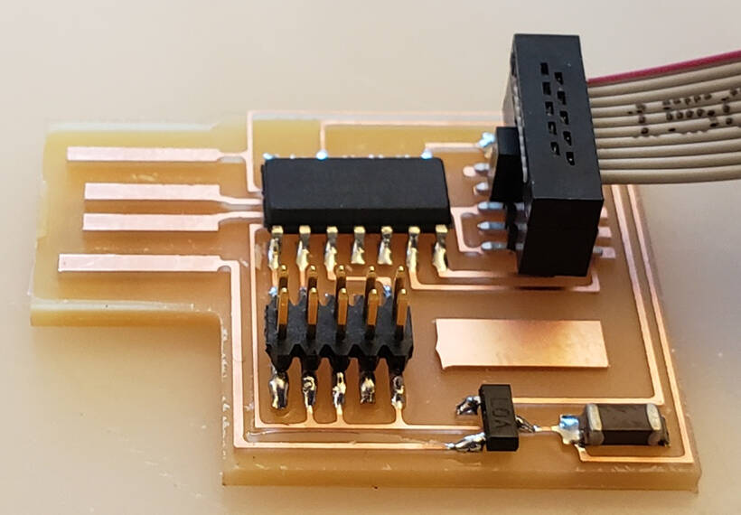
I scraped off some copper along the outer side of the USB to prevent it possible short-circuiting and below is how my UPDI board looked in the end:
I have to admit, my perfectionist self reeeeally wanted to make this board again. To try and do it all correctly this time, just so that ugly bypass wasn’t there anymore (*^▽^*)ゞ . However, I was actually one of the lucky ones that day, because many of the other students had a lot more issues with their soldering, lost traces, and connected legs (resulting in short-circuits). So, I should just be happy that it works, and hope that the bypass won’t fall off in the future.
Checking the Results
My board should now be ready for use, and so Henk plugged it into his laptop. The bypass and my other soldering work had apparently been successful, because the board was being picked up!
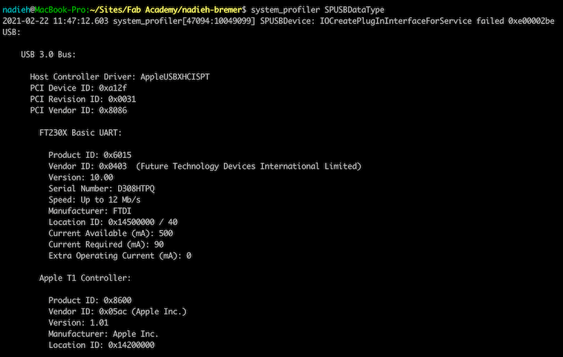
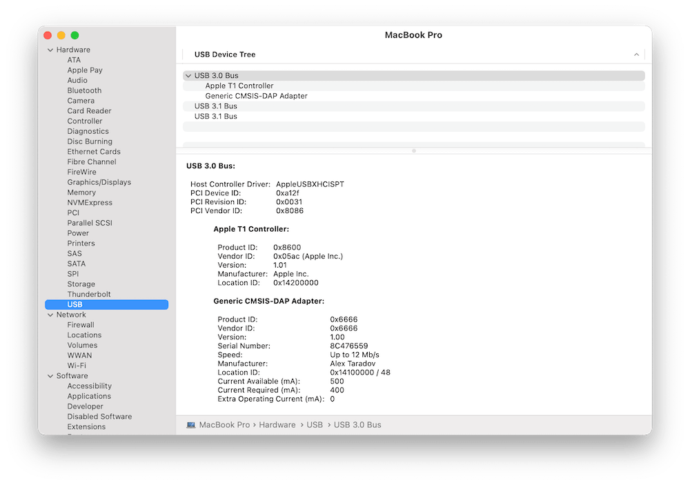
I plugged it into my own Mac. It wasn’t automatically registering as a USB that would appear in my Finder. However, when I went to the USB tab of the System Report (click on the top-left Apple icon, then on About this Mac and next on the System Report button in the window that appears) and it was registering there (ノ◕ヮ◕)ノ*:・゚✧

You can also get a list of everything connected to a USB from the terminal by running system_profiler SPUSBDataType
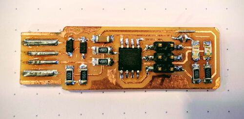
Bonus: Creating a JTAG Board
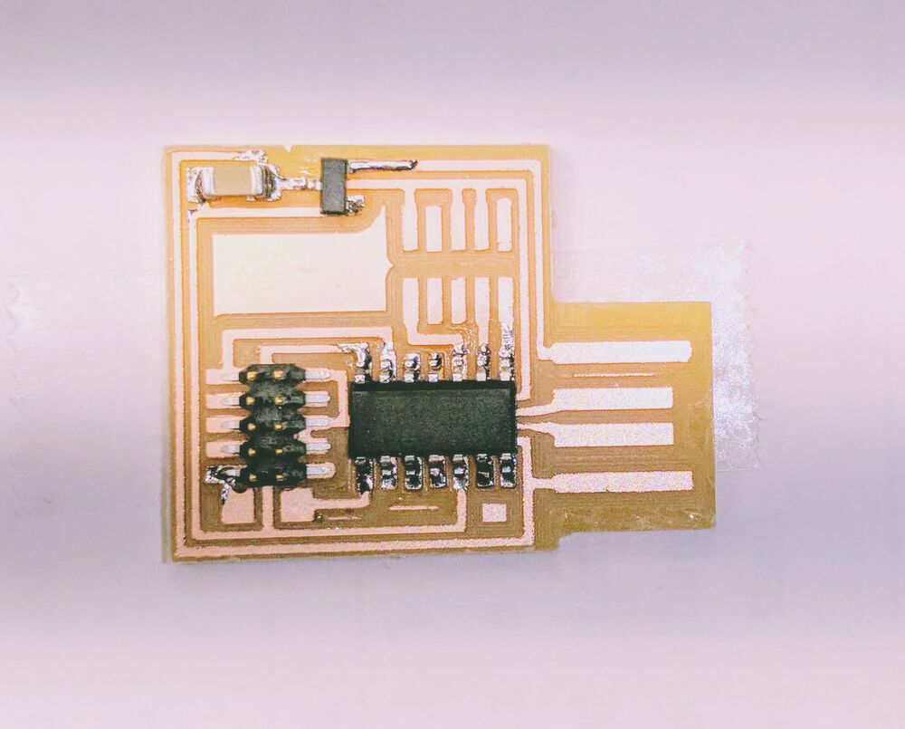
At this time it was a little before noon, and I had some time left. I really wanted to get more practice with the soldering, and therefore set-up to redo my UPDI board. However, Henk wanted me to make a JTAG board instead. The hello.CMSIS-DAP.10.D11C to be precise.
As I mentioned at the beginning, JTAG is a different protocol than UPDI, and thus making this board would make it possible for me to debug more types of boards(if I’ve understood things correctly).
Milling the JTAG PCB
I downloaded the traces and interior png files from the Fab Academy site.


I set-up the milling machine to first mill out the traces (with the 0.4mm single flute bit). After that was finished, I milled it out of the copper plate with the 0.8mm flute.


The traces of this board were definitely not as smooth as my first UPDI board. There were many burrs and the edges of the traces remained rather frayed even after sanding it with paper. I didn’t sand with a lot of force though, because I was afraid I might pull off a trace. The 0.4mm bit was definitely getting dull (it milled out one more board after mine, but that one was barely usable, before being replaced).
In retrospect it would’ve been better if I had set an offset of 5 in mods so the tiny copper strip that remained between the USB connector legs had been milled away.
Gathering the JTAG Components
I got the schematic and the example photo from the website as well. However, the photo was from the side and of low quality, so it was much less useful than the UPDI photo I had before.
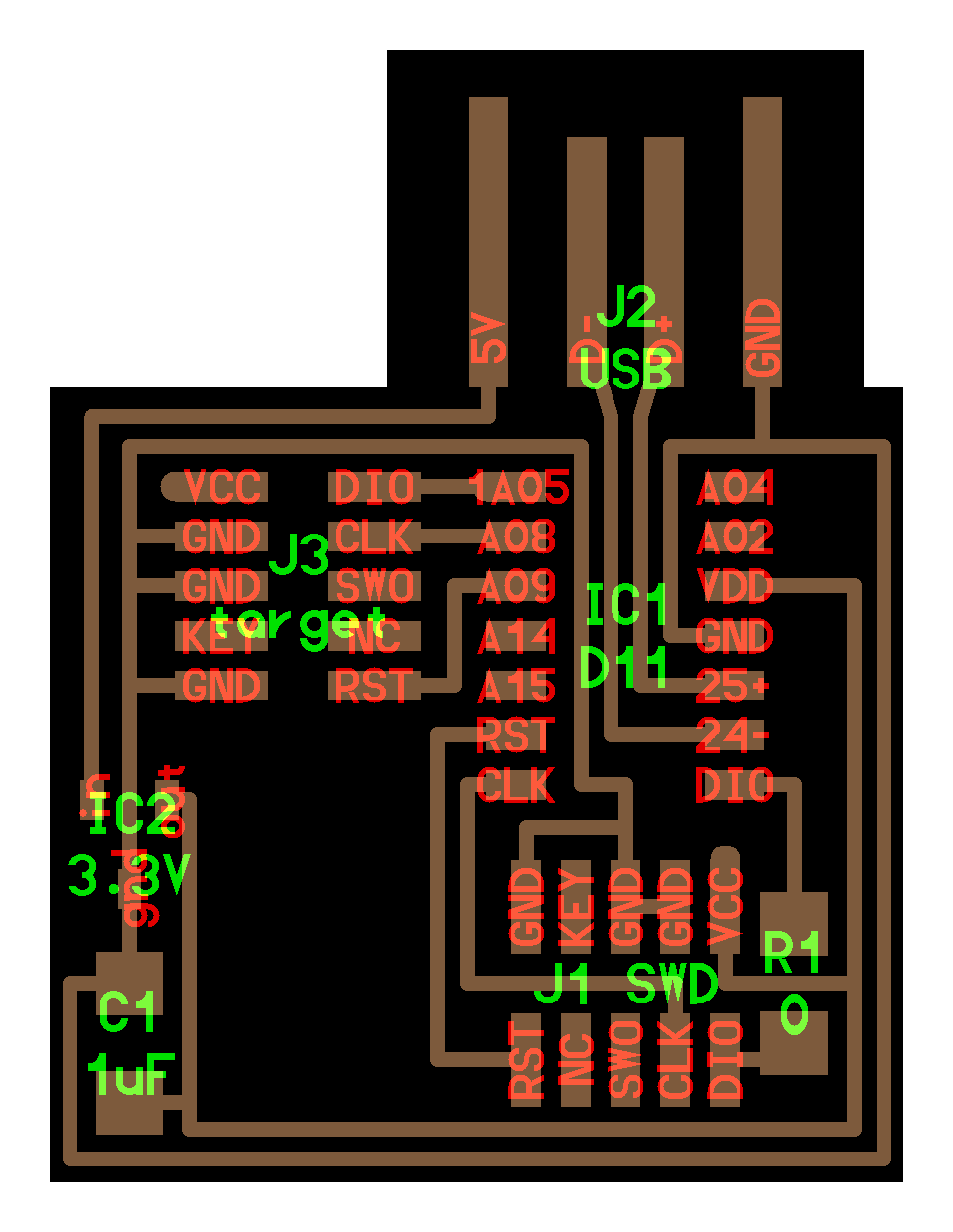
What turned out to be much trickier was the fact that many of the components mentioned in the schematic were totally unclear to me: J1 SWD? J2 target? Luckily, fellow student Loes was had gone through this a few hours before, and had found the right component names by checking the documentation of a previous Fab Academy student, and shared her result with me.
- R1: One resistor of 0 Ω
- C1: One capacitor of 1μF
- IC1: One integrated circuit, the D11, marked as a SAMD11C on the box
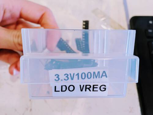
- IC2: One voltage regulator 3.3V, marked as 3.3V100MA LDO VREG. I don’t understand yet why a voltage regulator would be marked as IC, the same as the microcontroller. I guess a voltage regulator is also an integrated circuit? But gosh, this was tiny!

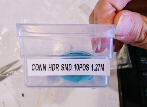
- J1 SWD & J3 target: Although they are both named differently on the schematic, they are both the same 10 pin component, marked as CONN HDR SMD 10POS 1.27M
The SAMD11C Microcontroller
To be honest, I did not do perform the steps to figure out what the correct orientation was for the SAMD11C chip. Instead I ended up being lucky that I had soldered on my SAMD11C microcontroller in the correct orientation.
Some Frustrations About This Week
The root of making this mistake is the fact that the students new to electronics (I for sure) don’t understand the what of what we’re doing this week. I now know how to mill a predefined PCB, and I learned how to solder. But what we’re making? Why it needs to be connected this way? What each component’s function is? I couldn’t really tell you.
And thus when we couldn’t find a clear white or indented dot on the SAMD11C, when the example photo doesn’t show a clear mark to signify that there’s a specific orientation for it, that the documentation from the previous student that was being used as reference made no mention of it, the fact that we were not taught in general how to know when a component can only be soldered on in one orientation, it was kind of assumed by all students in our lab making the JTAG that this chip could go on in both ways.
I know we can’t learn it all in just one week, so I guess we’re bound to make mistakes from basically “not knowing what we don’t know” every now and then.
Finding the Correct Orientation
Let me explain how I should’ve gone about this. While writing this documentation I found the write-up of yet another student who had created this JTAG board. Thankfully, his write-up is more complete, and taught me how to assess orientation.
First of all, there is a white dot on the chip. However, it’s easy to mistake as part of the text, it’s also more grey than white. I managed to make one (crappy) photo where you can kind of see it.
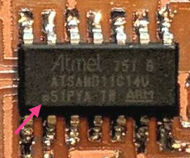
You download the datasheet of the SAMD11C from the manufacturer’s website (Microchip in this case). On page 8 of that document there’s a schematic of the chip (showing the white dot) and what each of the chip’s legs should be attached to. You can compare this to the schematic of the board to assess what direction of the chip should be.
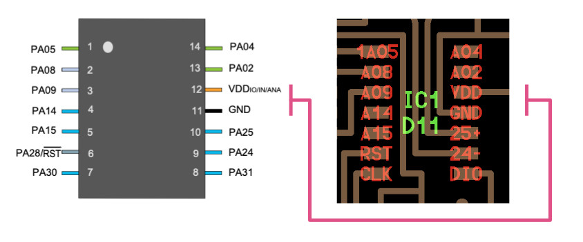
I don’t yet know what all the abbreviations mean, but I can at least see that some numbers are the same, and I figured that it would be very important to get the GND (ground) and I believe the VDD is quite important too, having something to do with the power supply(?), in the correct place.
Thus compared to the schematic of the full board that I was following, the white dot needed to be in the top-left position.
Soldering the JTAG Board
The legs of the components for this board were (just) far enough separated that each leg could be soldered separately, not having to use the “blob and suck away excess” method thankfully. I started with the central (and low) SAMD11C chip.
Especially at the start I was finding it difficult to put both my soldering iron onto the trace and leg plus add the solder to it. I kept on putting the solder onto the iron and not the trace. After a while I did find a method that was often successful: placing the tip of the iron on top of the leg, waiting a little, and then moving the solder towards it along the bottom, touching the trace right where the trace and leg met. It then naturally flowed underneath the leg and trace, fixing them together.

I continued with the tiny resistor and then the capacitor, which thankfully went well. I almost had the same issue with the resistor as I had with my UPDI; I thought I fixed it on one side, but hadn’t. Thankfully I remembered to check how firm the connection was, and noticed that I needed to solder that one side more before doing the 2nd side.
The lower-right 10-pin connector came next, then the resistor right next it, and finally the second 10-pin connector in the top-left of the board.
It wasn’t easy, but it was doable. I did seem to notice that my shaky hands had gotten worse since soldering the UPDI in the morning ಥ_ಥ (it was about 5 hours late at that point).
Checking the JTAG Soldering
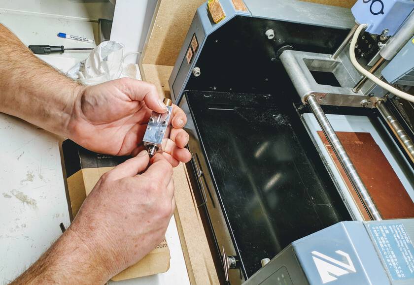
Next, stuff happened that I don’t understand. Apparently, the chip on the JTAG needed to be programmed before it would even show up when plugged into a computer, unlike my UPDI which (I guess) was already preprogrammed. Two of my fellow students were already done before me with their JTAG board and Henk was trying to program them.
He had created a set-up with a bunch of cables, and was using another JTAG board to test and program my board with I believe. I don’t know what he did, but at some point my board was showing up as having been programmed successfully in his terminal. Very happy to know that I had soldered this board correctly! (๑•̀ㅂ•́)ง✧
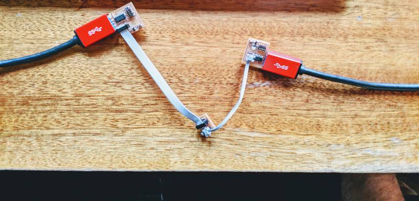
When I plugged the JTAG board into my own Mac it was thankfully now also showing up! (as CMSIS-DAP)

Reflections
Starting from a smooth copper plate, to a working printed circuit board, this was a very hands on week.
What went wrong
During the milling a lot went wrong during our group assignment, which I’ve already outlined in the “Milling Precision Test section. Thankfully, after all those mistakes with z-aligning, it went well for the two boards that I milled.
Another big mistake happened when I tried to remove the shoved capacitor from my UPDI board and in doing so also pulled up a tiny trace. I should’ve instead either known what to do in such a case, or asked Henk for advice. Although it’s always hard to tell when you should experiment on your own to fix it, and when you’re in a situation where it’s better to ask someone who knows what to do. But I guess that’s just part of making mistakes.
I’m not sure this last one belongs here, but I wish I understood what Henk did to program my JTAG board in a way that I could repeat the process. I know that he used one board to program another, but I wish I knew why the two boards were connected with a tiny board in between them, and what that Atmel-ICE (I think, after seeing it appear in the write-up of one of the previous students) was doing there. (The “programming” section of this write-up of yet another previous student might come in handy at some point?)
What went well
Apart from one mistake that almost cost me the entire UPDI board, I’m quite happy with how well the soldering went, especially seeing as how I’d never done it before. No issues with legs that I couldn’t separate, or short circuits, or the board not working without a clear reason as to why. I’m also pleased that I had the time to create a second board, the JTAG next to my UPDI.
What I would do differently
Some of the main lessons I learned this week:
- I need to be even more vigilant in the exact steps that our instructor follows when operating the machine. Even the seemingly insignificant steps can be of vital importance. If you don’t understand why something is done the way it is, first ask why before assuming “to do it a different way, because it seems to extrapolate that way”.
- Check each soldered component after having fixed it in place with one side to see if it’s placed firmly enough.
- Perhaps check some tutorials about how to use soldering wick since I felt that the vacuum pump might/could be too big to get rid of all the excess solder when soldering tiny tiny legs. This Ultimate Guide to Desoldering seems like a good place to start.
- Or perhaps I should use a soldering iron and non-heatable vacuum pump, instead of the vacuum pump that gets hot, when dealing with issues where the vacuum pump’s nozzle is too large to really be pushed against the solder to heat it up? With the soldering iron and its tiny tip I could heat up the solder, which can then be sucked away with the pump.
Wrapping up
This was the first week of the Fab Academy where I felt totally lost in terms of the material we needed to learn. The other weeks had at least had something that seemed somewhat familiar. But basically every term and process of this week was new to me. And that also made it a bit of a frustrating week. Because I really wanted to understand what we were making and what it would do. It felt wrong to just make something where you don’t understand its reason for existence, or what the separate parts even do. I googled the words UPDI, JTAG, ISP and whatnot, to find introductions and try and learn it on my own, but the only results I got were how to make them, not the basic reason for them (maybe I was just searching for the wrong words). To conclude, I’m looking forward to the week in which I’ll learn what the heck I made ✖‿✖