This week we learned how to communicate between two devices/microcontrollers and I took the opportunity to use this week to design a board that I can use for my final project, eventually turning into three separate boards, all hexagonal shaped of course.
Assignments
Our tasks for this week are:
- Group assignment: Send a message between two projects
- Individual assignment: Design, build, and connect wired or wireless node(s) with network or bus addresses
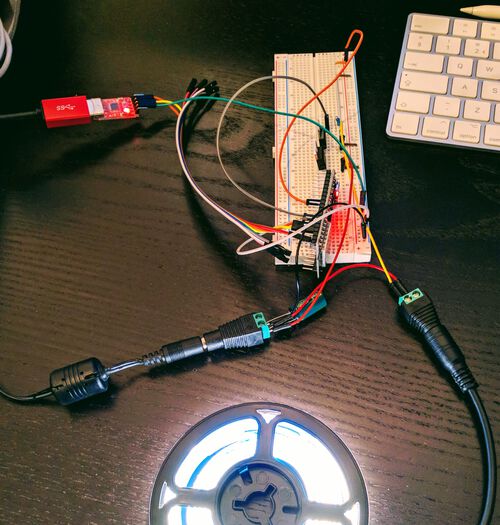
Hero Shots
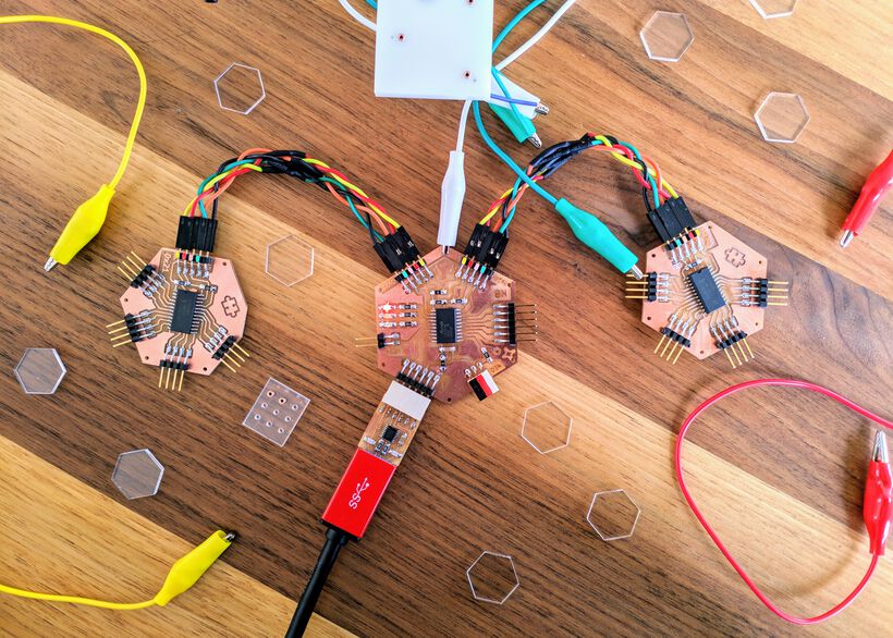
Showing some final results of my hexagonal boards & the ESP32 + LED strip for the tl;dr and hopefully showing you why the rest of this very long blog could be interesting to read (⌐■_■)
Ways of Communicating
At the start of the instruction day at the lab, Henk explained three (often-used) protocols with which devices can communicate with each other; asynchronous serial, SPI, and I2C.
Because I think it’s useful to keep the acronyms MISO and MOSI, I’ll be using Manager/Staff instead of Master/Slave in this documentation.
Asynchronous Serial
Serial communication is what we’ve been using already using the TX and RX connections between our boards and the FTDI, and the Serial Monitor in our laptop where we could see the Serial.print() statements (e.g. to print the value from a sensor).
The asynchronous part means that data is transferred without the support from an external clock. This means that some base rules are needed for the two devices to be able to communicate:
- Baud rate | This specifies how fast data is being sent over the serial line, usually expressed as bits-per-second (bps). Inverting the bps tells you how long it takes to transmit a single bit. I’ve generally been using a baud rate of
9600, because speed wasn’t critical. The highest speed generally is115200, however the chance for errors gets greater the faster you’re sending. - Synchronization bits | These are the start and stop bits, which mark the beginning and end of a packet, which is (usually) a byte of data. A serial line idles in HIGH, meaning when nothing is being sent it is held at the value
1. The start bit will transform the line from1to0, while a stop bit will move it back by holding the line at1again. - Data bits | This is the real information that the processor wants to send. It’s generally called a data chunk because the exact size (in bits) isn’t fixed, it can be anything from 5 to 9 bits, but the standard is 8 bits.
- Often, the order in which the bits is send is LBS or least-significant bit first (e.g. the character a has a binary value of
01100001, and is being send as10000110)
- Often, the order in which the bits is send is LBS or least-significant bit first (e.g. the character a has a binary value of
- Parity bits | This comes down to a very simple error-check done for each frame being send. First, all the data bits are added up. Next, check if this sum is even or not. If the parity mode is set to even, and the sum of the data bits has an odd number of
1s, then the parity is set to1to make the total even again. While if the parity mode was set to odd, then the parity bit would be set to0in this case. The error-check then comes down to the receiver checking that the parity bit has been set correctly, based on the data it received before. If it’s wrong, then some error has occurred in the transmission and the whole frame (or whole message even?) is ignored.- Parity bits are optional. They slow down the data transfer and often isn’t used except for noisy mediums.

It’s important to remember to connect the TX of the Manager to the RX of the Staff, since what is a transmission of one device is received by another (think of it like a phone).
To be able to do serial communication a Universal Asynchronous Receiver & Transmitter or UART is required. A computer can talk to a UART in parallel, which is then transformed into serial. Generally the datasheet will tell you if a UART is part of the hardware.
You can also use software to turn any GPIO port into a TX or RX port, such as the SoftwareSerial library in the Arduino IDE. However, this takes up both memory and computing time, so should only be done if the processor doesn’t have a UART already (or you need more TX and RX ports).
The downside of using serial communication is that there’s extra overhead in the extra start and stop bits (and possible parity bit), and it apparently requires complex hardware. Furthermore, it’s really only designed to communicate between two devices. If more than two devices are connected, you could get issues where two of them are trying to transmit at the exact same time, resulting in a conflict on the line.
One configuration that can work is that the Manager is only transmitting (along its TX line), and that any Staff are thus only receiving (along their RX lines). You give each Staff member its own ID or address and make the first bit this ID. All Staff members will then compare that first bit against their own ID and for the one Staff member where it’s correct, you continue to do things with the rest of the incoming data, while all the other Staff members will ignore the rest of the incoming data.

See this page on Sparkfun for more information about serial communication.
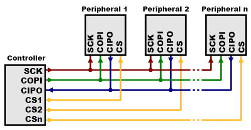
SPI
Serial Peripheral Interface is a synchronous way of communicating; there is a line to send data and one for a clock, the SCK line, that keeps both sides in sync. This clock oscillates and tells the receiver exactly when to sample the bits on the data line.
The start of a frame comes from a change in the line, from 0 to 1 or vice versa. It depends on the exact device what it sees as idle. The receiver will merely listen for an edge, a change from the idle state.
With SPI only one processor will generate the clock signal, this is the Manager, while all devices/peripherals at the other side are the Staff. Data that is being send from the Manager to a Staff member is send along the MOSI line, Manager Out / Staff in. When the Staff wants to send something back, it comes along the MISO line, Manager In / Staff Out.
For sending back a large amount of data from the Staff to the Manager, you might need to use the first frame to tell the Manager how many clock cycles it should generate to get it all, but this is a more advanced thing I believe.
The last of the lines with SPI is the SS or Staff Select. This is the Manager’s way of saying which Staff member should start listening when it sends data across the MOSI line. Generally the SS line is idle as HIGH. Just before data is sent to the Staff member, the line is brought low, which activates it. When the Manager is done, the SS line is made high again.
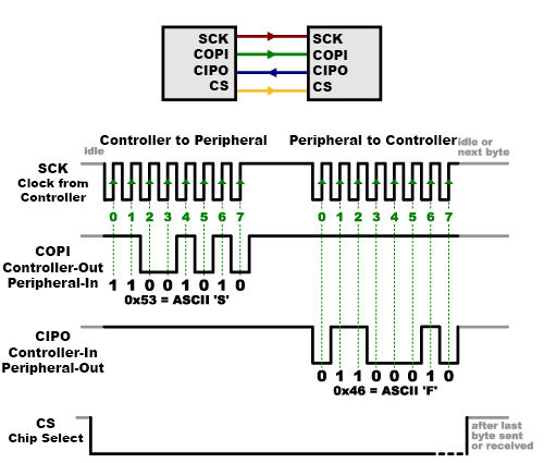
To add multiple Staff members, each will generally get its own SS line. To talk to a particular Staff member, you’ll make their SS line low and keep the other SS lines high.
In terms of programming you use the shiftIn() and shiftOut() commands. There is also an SPI library for the Arduino IDE that takes advantage of the SPI hardware built into a microcontroller.
See this page on Sparkfun for more information about SPI.
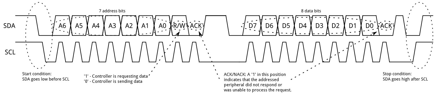
I2C
Although SPI is popular, the Inter-Integrated Circuit (I2C) protocol is taking over because you need fewer pins; only two, no matter how many Staff you’re connecting (up to 1008). I2C also allows for more than one Manager, which SPI can’t do.
The two lines of I2C are SDA, the data signal, and SCL, the clock signal. As with SPI, the clock signal is generated by the Manager. Generally, both the SDA and SCL line are connected to VCC with ±5kΩ resistors to restore the lines to HIGH when no device is actively trying to pull it LOW.
Within the I2C protocol messages are split into two types of frames:
- Address frame | In this frame the Manager will indicate which Staff member it wants to send data to. It is always the first frame in any new communication sequence.
- For a 7-bit address, the address is send out most significant bit (MSB) first, followed by a R/W bit indicating whether this is a read (
1) or write (0) operation. - The 9th bit of the frame is the NACK/ACK bit ((not)-acknowledge). This is the case for all frames (data or address). Once the first 8 bits of the frame are sent, the receiving device is given control over SDA. If the receiving device does not pull the SDA line LOW before the 9th clock pulse, it’s assumed that the receiving device either didn’t receive the data or didn’t know how to parse the message. In that case, the exchange halts, and it’s up to the Manager of the system to decide how to proceed.
- For a 7-bit address, the address is send out most significant bit (MSB) first, followed by a R/W bit indicating whether this is a read (
- Data frame(s) | These 8-bit frames contain the data being send. This is send along the SDA line by either the Manager or the Staff, depending on whether the R/W bit in the address frame said it should be read or write.
There is a start condition; To initiate the address frame, the Manager device leaves SCL HIGH and pulls SDA LOW. This puts all the Staff members on notice that a transmission is about to start.
Once all the data frames have been send, the Manager will generate a stop condition. These are defined by a LOW to HIGH transition on the SDA line after a HIGH to LOW transition on the SCL line, with the SCL remaining at HIGH (thus during any data transmission, the SDA line should not change when SCL is HIGH).
To program with I2C you can use the Wire library in the Arduino IDE.
See this page on Sparkfun for more information about I2C and the more complex ways of communicating, such as 10-bit addresses, repeating start conditions and clock stretching.
Experimenting With Protocols
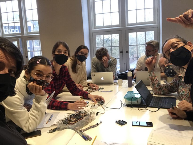
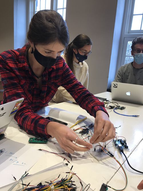
For the first time this Fab Academy, all eight of us sat together around two large tables to do a group assignment together (it’s always been split into at least two groups before). We wanted to get a first try at doing communication between three devices using I2C and Serial.
An I2C Network
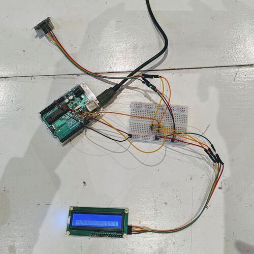
We started with I2C because Erwin, the electro-engineer of our group, said it would be the easier of the two. Using an Arduino Uno as the Manager, we also had a SDD1306 OLED screen and a HD44780 LCD display that would become the Staff.


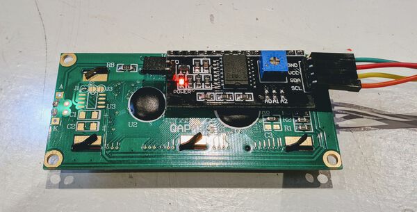
Both peripherals thankfully had clearly labelled pins with VCC, GND, SDA, and SCL, which we hooked up to a breadboard (each pin type got its own color), while the breadboard also had wires coming from the Arduino Uno.

Erwin was in charge of programming the Arduino / Manager. He started out by writing a script that would try and find the addresses of the LCD and OLED screens. The script basically calls for each possible address and sees if any device responds:
#include <Adafruit_I2CDevice.h>
Adafruit_I2CDevice i2c_dev = Adafruit_I2CDevice(0x10);

void setup() {
  Serial.begin(115200);
}//void setup

void loop() {
  Serial.println("I2C address detection test");

  // Loop through all possible i2c addresses
  for (char i = 0; i < 127; i++) {
    // Send address
    Adafruit_I2CDevice i2c_dev = Adafruit_I2CDevice(i);

    // If response on address, print address
    if (i2c_dev.begin()) {
      Serial.print("Device found at 0x");
      Serial.println(i2c_dev.address(), HEX);
    }//if
  }//for i
  // Wait 5 seconds, then rescan
  delay(5000);
}//void loop
At first the script ran to 255 instead of 127 and returned 4 possible devices: 0x27, 0x3C, 0xA7, and 0xBC. Thankfully it was quickly figured out that 0xA7 is 128 steps beyond 0x27 and 0xBC is 128 steps beyond 0x3C. We’d therefore cycled through the same addresses again.
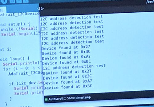
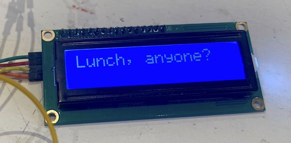
Unplugging one device, seeing which address remained showed us that the LCD display had 0x27 as its address and the OLED screen was 0x3C.
We started with the LCD display. Using the hd44780 library for the Arduino IDE, Erwin loaded the Hello World example

The bare bones code, with almost all comments removed came down to this:
#include <Wire.h>
#include <hd44780.h>                       // main hd44780 header
#include <hd44780ioClass/hd44780_I2Cexp.h> // i2c expander i/o class header

//Create LCD object at i2c address
hd44780_I2Cexp lcd(0x27);
//LCDs geometry
const int LCD_COLS = 16;
const int LCD_ROWS = 2;

void setup() {
  int status;

  status = lcd.begin(LCD_COLS, LCD_ROWS);
  if(status) {
    hd44780::fatalError(status); // does not return
  }//if

  // Print a message to the LCD
  lcd.print("Hello World");
}//void setup

void loop() {}
Which wrote Hello, World! in the LCD display:

For the OLED screen, Erwin used the demo example from the Adafruit SSD1306 library, the ssd1306_128_32_i2c. I won’t share the code of this example here, because it’s quite long, but you can find it in the library. However, the only change required was setting the screen’s address with #define SCREEN_ADDRESS 0x3C

Having defined both an LCD and OLED screen through their address with a variable lcd and display, respectively, it was quite straightforward to send commands to both. Erwin simply copied the libraries and setup code of the LCD into the OLED example. He then placed lcd.clear() and lcd.print() statements before each of the changes in the OLED demo, making it show in words what the OLED was showing on the screen. A snippet of the code:
  //Tell the LCD to show the word "Rectangles"
  lcd.clear();
  lcd.print("Rectangles");
  //Two functions from the OLED demo that draw rectangles
  testdrawrect();      // Draw rectangles (outlines)
  testfillrect();      // Draw rectangles (filled)

  //Tell the LCD to show the word "Circles"
  lcd.clear();
  lcd.print("Circles");
  //Two functions from the OLED demo that draw circles
  testdrawcircle();    // Draw circles (outlines)
  testfillcircle();    // Draw circles (filled)
Which looked like this:
A Serial Network
For the asynchronous serial network, I plugged the LED board that I’d made last week, and Nicole’s board into the breadboard, using the VCC, GND, TX and RX connections on the FTDI pins, and switched the Arduino Uno from using its SDA and SCL pins to the TX and RX pins.
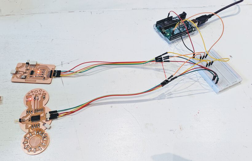
Erwin wrote the following code for the Manager/Arduino to continuously switch between sending something to Nicole’s board (which we defined to be 1) and my board (defined to be 2):
// Define client addresses
#define CLIENT1 1
#define CLIENT2 2

// Define client commands
#define STOP  0x04
#define START 0x08

void setup() {
  Serial.begin(9600);
  pinMode(LED_BUILTIN, OUTPUT);
}//void setup

void loop() {
  // Turn LED off (to indicate client1)
  digitalWrite(LED_BUILTIN, HIGH);

  // Send command START to CLIENT1
  // Note: this code is somewhat wrong, it should all be Serial.write()
  Serial.print(CLIENT1, BIN); // Send address for client 1
  Serial.print(START, BIN);   // Send the command

  // Wait 5 seconds
  delay(5000);

  // Turn LED on (to indicate client2)
  digitalWrite(LED_BUILTIN, LOW);

  // Send command START to CLIENT2
  Serial.print(CLIENT2, BIN); // Send address for client 2
  Serial.print(START, BIN);   // Send the command

  // Wait 5 seconds
  delay(5000);
}//void loop
Note | As I discovered during the “Mechanical & Machine Design” week, we again were stumped for a bit that we couldn’t upload to the Arduino. This was because we’d connected the TX and RX to the two other boards. To upload to the Arduino, these two wires had to be disconnected.
I grabbed my laptop to be able to program both boards using the UPDI connection. Erwin gave me some code that would read any incoming serial data, check if the first bit was the same as the address of the board, if yes, “do something, if not, “do nothing”. I adjusted that to turn on the green LED om my board if the incoming data had my board’s address, turn on the red LED of there was something coming in, but wasn’t for my board, and turn on the blue LED if no serial message was being received.
At first however, my board kept showing a blue LED; indicating that it wasn’t receiving any serial. We therefore grabbed a logic analyzer, plugged a channel into the breadboard (along the TX line) and another into GND, connected the analyzer to Nicole’s laptop and started following where the bits were lost.
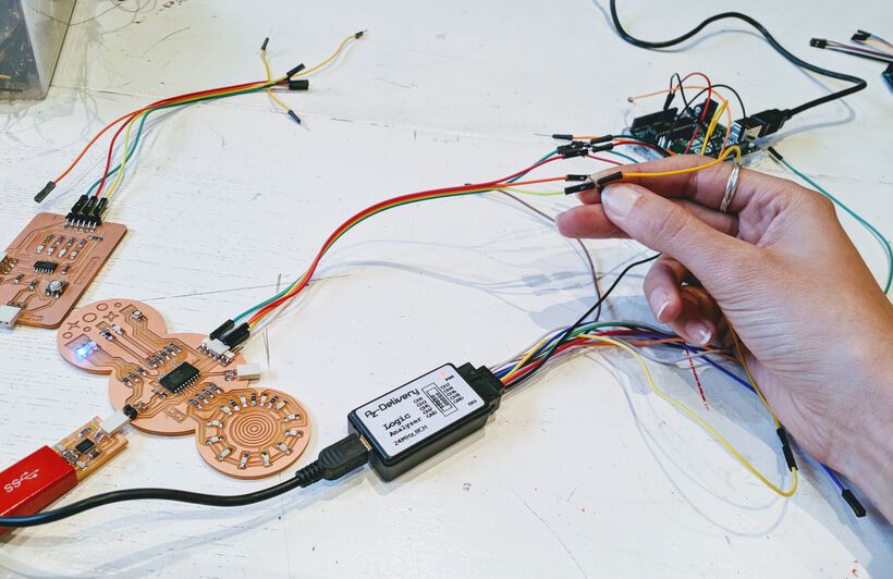
The first thing we learned was that I’d mixed up the TX and RX wires on the two boards, oops, classic mistake!
After that the LED on my board turned to red, indicating that it was receiving serial, but it was never meant for my board. I had to use a delay in the loop function though, otherwise you couldn’t see the red LED blinking because it was over so fast.
Using the logic analyzer we set the Async serial over the channel to decode the bytes, which showed us that strangely the incoming bytes that defined the addresses were 0x31 and 0x32, not a back-translation to 1 and 2 as Erwin’s code had send.
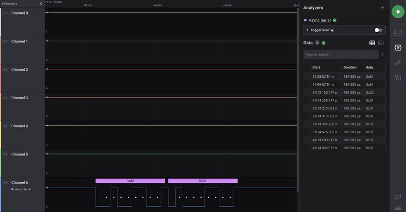
It appears that 1 is 0x31 and 2 is 0x32 in hexadecimal, but for my board to think that the incoming address was correct, I truly had to set #define myAddress 0x32. However, after that my board started to respond to the messages with a green LED turning on every few seconds as well.
I uploaded the same code to Nicole’s board as well, only changing the address to 0x31 and updating the pin numbers for the red, green, and blue LEDs.
Strangely, the boards started blinking out of sync several seconds after having (re)started both of them. We weren’t able to figure out why though.
Erwin tried several things to see if the bytes being received by our boards would change to 1 and 2, such as sending the address as a byte, #define CLIENT2 0b00000010, but nothing made a difference. I have to admit that I didn’t follow everything that Erwin was trying, but in the end he had to give up and we just stuck with 0x31 and 0x32 as addresses on the two boards ┐( ̄ヮ ̄)┌
Note | Days later Erwin managed to solve what was the issue; he’d been using Serial.print() to send messages, and should’ve been using Serial.write().
Below is the generic code that was uploaded to my and Nicole’s board (Nicole’s board having a 0x31 address and different pin numbers for het red, green and blue LEDs):
#define myAddress 0x32 //Hardcoded this to be "my" address

#define PIN_LED_R 16
#define PIN_LED_G 0
#define PIN_LED_B 1

void setup() {
  Serial.begin(9600);
  //R, G & B LEDs
  pinMode(PIN_LED_R, OUTPUT);
  pinMode(PIN_LED_G, OUTPUT);
  pinMode(PIN_LED_B, OUTPUT);
}//void setup

void loop() {
  //Reset the pins
  digitalWrite(PIN_LED_R, LOW);
  digitalWrite(PIN_LED_G, LOW);
  digitalWrite(PIN_LED_B, LOW);
  byte incomingByte;

  if (Serial.available() > 0) {
    //Read the incoming byte:
    while (Serial.available()) { incomingByte = Serial.read(); }

    if (incomingByte == myAddress) {
      if (Serial.available() > 0) {
        //Read the incoming byte:
        while (Serial.available()) { incomingByte = Serial.read(); }
        //This is me! Do something
        digitalWrite(PIN_LED_G, HIGH);
      }//if
    } else {
      if (Serial.available() > 0) {
        //Read the incoming byte:
        while (Serial.available()) { incomingByte = Serial.read(); }
        //This isn't me... Do nothing
        digitalWrite(PIN_LED_R, HIGH);
      }//if
    }//else
  }//if
  else {
    //I'm not receiving any serial data
    digitalWrite(PIN_LED_B, HIGH);
  }//else

  delay(1000);
}//void loop
Designing My Board
My goal for this week was to create the board(s) that I’d need for my final project. In the “Input Devices” week I’d decided that each of the puzzle pieces would act as a simple switch so I’d know which places on the board were already filled. This meant that each puzzle piece would have to be connected to its own pin on the microcontroller. However, since I wanted to create between 16 - 50 puzzle pieces, I would need a way to expand the number of GPIO pins on a microcontroller.
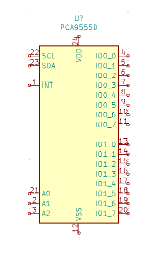
PCA9555D
Henk told me that this can be done with multiplexing, and that a previous student, Harm, had required the same GPIO pin expansion. From Harm’s documentation I saw that he’d used a PCA9555D, which is labelled as a 16-bit I2C-bus and SMBus I/O port (I’d call that an “IO port expander” in easier-to-understand words).
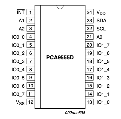
The PCA9555D uses I2C to give you access to 16 more GPIO pins, which can be set as both input and output.
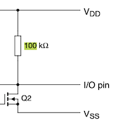
Since I wanted to use these pins basically as switches I had to check if there were internal pullup resistors inside the PCA9555D, or if I’d had to add these externally. Without such resistors there would be too much noise on the line.
A quick online search led me to a forum that mentioned that each GPIO pin is connected to an internal 100kΩ resistor. Looking in the datasheet I was indeed able to find an image that showed this resistor, although I got the sense that it’s not quite explicitly mentioned in the text itself.
I did a general online search for the PCA9555D to find examples of how its used in schematics, and I could start to understand how to connect the non GPIO pins. From Harm’s documentation I also saw that the datasheet itself shows an example:
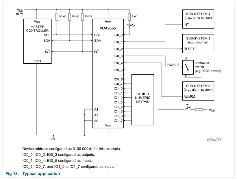
From that I wasn’t totally sure what the INT pin was, except that it also went back to the main microcontroller, and had an external pullup resistor. Thankfully, Harm had already figured it out and explained in his documentation: “The open-drain interrupt output (INT) is activated when one of the port pins changes state and the pin is configured as an input. The interrupt is de-activated when the input returns to its previous state or the Input Port register is read”
Which I understood to be a pin that I could “listen” to to check if any of the GPIO pins had seen a change in state (HIGH to LOW or vice versa).
From the example schematic I also saw three A pins, which all went to GND. This I thought was a bit odd, why have three pins to only have them connect to GND? Many other schematics that I found online also had all three A pins connected to GND.
From the datasheet those A pins were called address input. That seemed important, but I didn’t understand it yet. In my online search to figure out what it meant, I found a second datasheet from Texas Instruments, which held some valuable information about the address part in particular that wasn’t as well explained as in the NXP datasheet I linked to before.
For example, its definition for the A pins was “Address input. Connect directly to VCC or ground”. Ah, it was starting to dawn on me.
Searching the datasheet further I found the explanation, the A pins were the way you gave the PCA9555D its address through the combination of which was connected to GND and 5V. Smart, that way you could combine up to 8 (3-bit) different ones.

I’d already been wondering how I would be able to combine multiple PCA9555D devices without an overlap in address.
I felt like I understood the PCA9555D enough now to start incorporating it in my KiCad schematic.
All Required Components
Before I could work on my KiCad schematic though I had to first know how many puzzle pieces my puzzle would truly have, since this would tell me if I’d need two or three PCA9555Ds.
I therefore first drew my final puzzle pieces, which you can read about on my “Final Project page”, and came to a total of 38 pieces.
I’d prefer to have two PCA9555Ds instead of three to lower the complexity of wiring them. With two I’d have 32 GPIO pins, so I’d need 6 more pins. I figured I could go with the ATtiny3216 for my main microcontroller, to have the biggest Flash and SRAM memory of the ATtiny’s available in the lab (I think?), plus use 6 of its GPIO pins for the puzzle pieces.
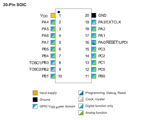
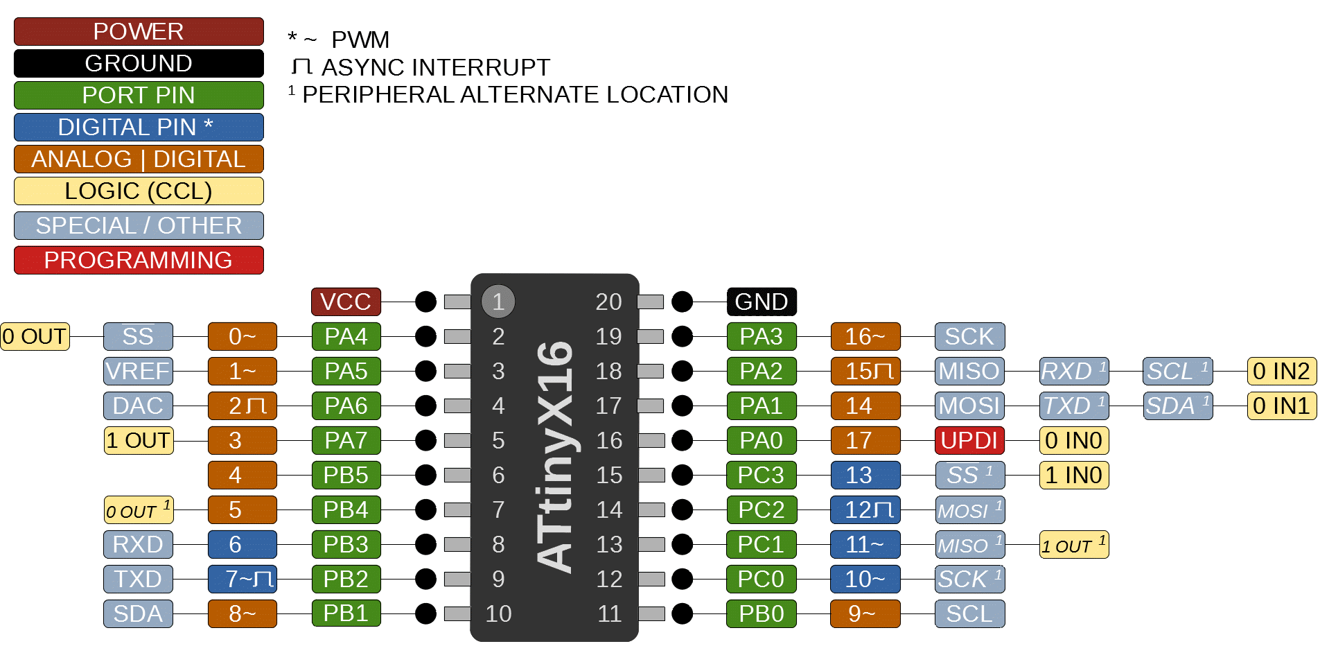
This was the same microcontroller as I’d used last week, and thus I already had the pinout from the ATtiny3216’s datasheet and the Arduino version of the pinout from the megaTinyCore website available:
For the connection with the PCA9555D I’d need the SDA and SCL pins of the ATtiny3216, but I also wanted to still use the TX and RX, the UPDI for programming, and one pin for the NeoPixels.
In the end I saw that I needed 16 out of the 20 available pins, and threw in three LEDs for good measure (and very useful indicators to check your programming without the need of looking at the Serial Monitor (e.g. make an LED blink if X occurs)):
| Component | ATtiny3216 Pin Number | Arduino Pin Number | Note |
|---|---|---|---|
| LEFT SIDE | |||
| VCC | 1 / VCC | ||
| NeoPixels | 2 / PA4 | 0 | PWM |
| Puzzle Pin | 3 / PA5 | 1 | PWM |
| Puzzle Pin | 4 / PA6 | 2 | |
| Puzzle Pin | 5 / PA7 | 3 | |
| Puzzle Pin | 6 / PB5 | 4 | |
| Puzzle Pin | 7 / PB4 | 5 | |
| Puzzle Pin | 8 / PB3 | 6 | Digital only |
| INT (0x20) | 9 / PB2 | 7 | PWM / Digital only |
| SDA | 10 / PB1 | 8 | PWM |
| RIGHT SIDE | |||
| GND | 20 / GND | ||
| - | 19 / PA3 | 16 | PWM |
| TX | 18 / PA2 | 15 | Alternate TX position |
| RX | 17 / PA1 | 14 | Alternate RX position |
| UPDI | 16 / PA0 | 17 | |
| LED | 15 / PC3 | 13 | Digital Only |
| LED | 14 / PC2 | 12 | Digital Only |
| LED | 13 / PC1 | 11 | PWM / Digital Only |
| INT (0x21) | 12 / PC0 | 10 | PWM / Digital Only |
| SCL | 11 / PB0 | 9 | PWM |
The table above already takes into account the exact pin numbers that I used for my final schematic (Apart from 5V, GND, SDA and SCL I moved literally everything else around while trying to lay out the boards in KiCad).
Schematic in KiCad
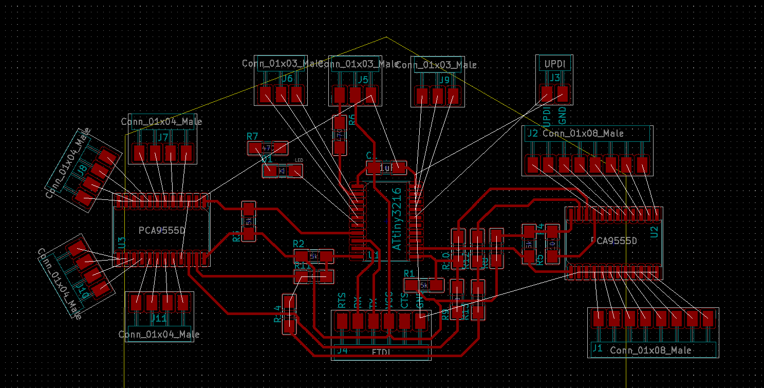
I opened KiCad and started designing my board with the Schematic Layout Editor while following the steps from my “Electronics Design” documentation.
Thankfully, the PCA9555D is available in the default KiCad library that I’d installed during the “Electronics Design” week, so that was no hassle to add (I’ve actually never really had to look online for a missing symbol/footprint).
At first I connected the two sets of GPIO pins (on the right of the symbol above) to Conn_01x08_Male connectors, however, during the PCB layout of the board I realized that I couldn’t make it work with 8 pins all side by side, traces would have to run too close together, and therefore split them up into Conn_01x04_Male connectors instead.
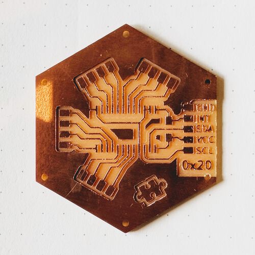
Below you can see the final schematic from KiCad, reflecting my actual board. I’ve highlighted some of the major areas (outside of the ATtiny3216 in the upper-left). Having come from requiring eight 0Ω bridges at some point (⊙0⊙) to only needing two, I’m proud of myself (•ω•)
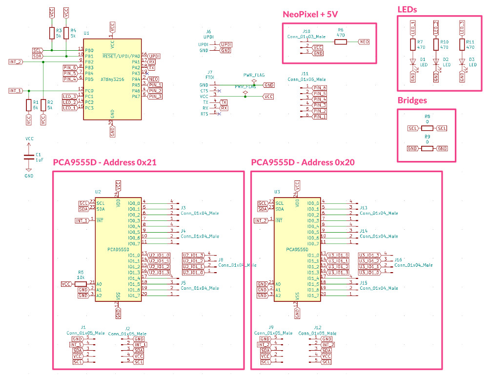
Below is a table with the components used:
| Component | Full Label in KiCad | Reference | Specific Orientation |
|---|---|---|---|
| ATtiny3216 | Microcontroller_ATtiny3216-SFR | U1 | Yes - Dot in one corner |
| 2x PCAA9555D I2C GPIO expander | PCAA9555D | U2 & U3 | Yes - Dot in one corner |
| 1x 01x03 Female connector | Conn_01x03_Male (I couldn’t find a female symbol in the fab library) | J10 | Yes |
| 8x 01x04 Male connector | Conn_01x04_Male | J3, J4, J5, J8, J13, J14, J15, J16 | Yes |
| 4x 01x05 Male connector | Conn_01x05_Male | J1, J2, J9, J12 | Yes |
| 1x 01x06 Male connector | Conn_01x06_Male | J11 | Yes |
| UPDI | Conn_UPDI_01x02_Male | J6 | Yes |
| FTDI | Conn_FTDI_01x06_Male | J7 | Yes |
| Capacitor 1μF | C_1206 | C1 | No |
| 3x LED - various colors | LED_1206 | D1 - D3 | Yes - Green marking on top pointing to cathode |
| 11x Resistors - various values | R_1206 | R1 - R11 | No |
PCB Layout in KiCad
I felt that the schematic looked quite straightforward. However trying to make this layout work in the PCB Layout Editor took FOREVER! It was my whole Sunday basically, from 10 in the morning to 10 in the evening before I had something functional [¬º-°]¬
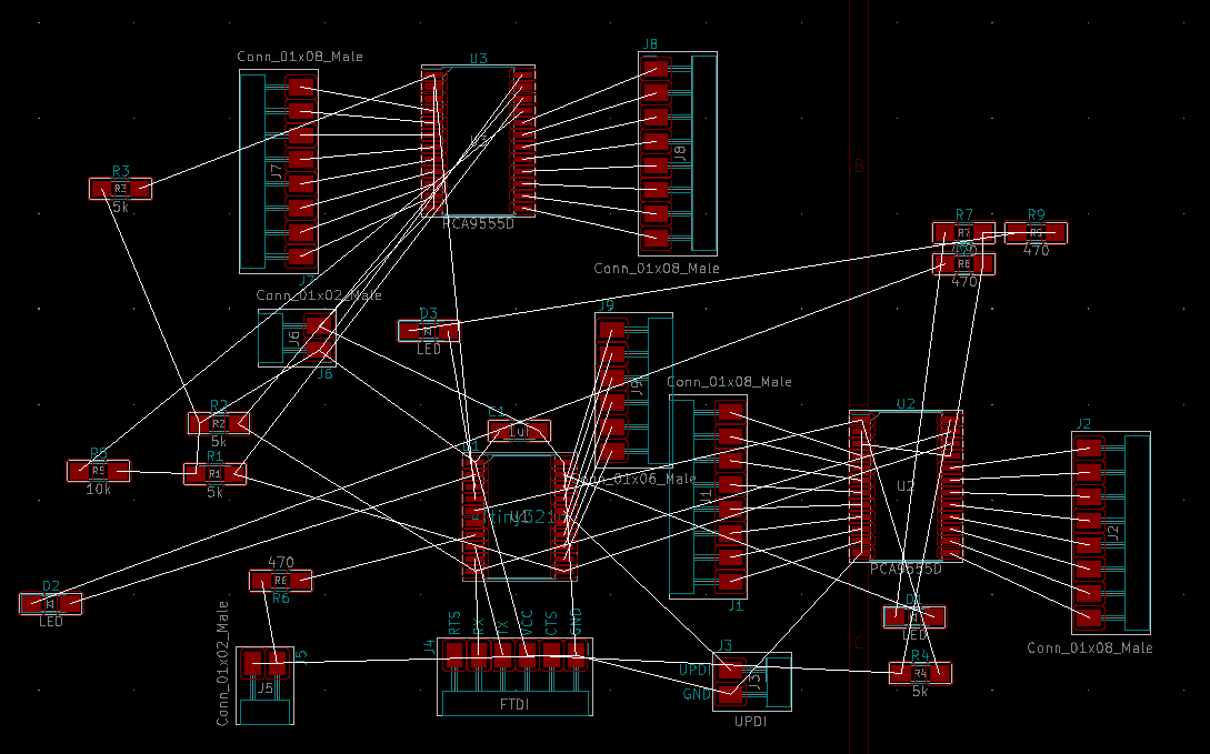
One part of that problem was space. Besides the 38 male connectors that should go to the puzzle pieces, I also required 5 for the FTDI, 2 for the UPDI and 3 for the NeoPixels and 5V and GND for the eventual 5V adapter that would power my board. In short, I needed the perimeter of my board big enough to fit 48 connector pins.
I naturally first aimed to fit it all into one big hexagon. In my head this idea worked quite well, because I’d use four of the six sides for the 8-pin connectors of each side of the PCA9555Ds, and use the remaining two sides for the 6-pin connector (for 6 last puzzle pieces) + 2-pin UPDI, plus the 5-pin FTDI + 3-pin NeoPixel & power connectors. It was perfectly in balance then.
Sadly though, I realized early on that this layout wouldn’t be able to fit on the copper plates available in the lab (which are 127x102mm), I’d need closer to 140x140mm ( ̄ー ̄)
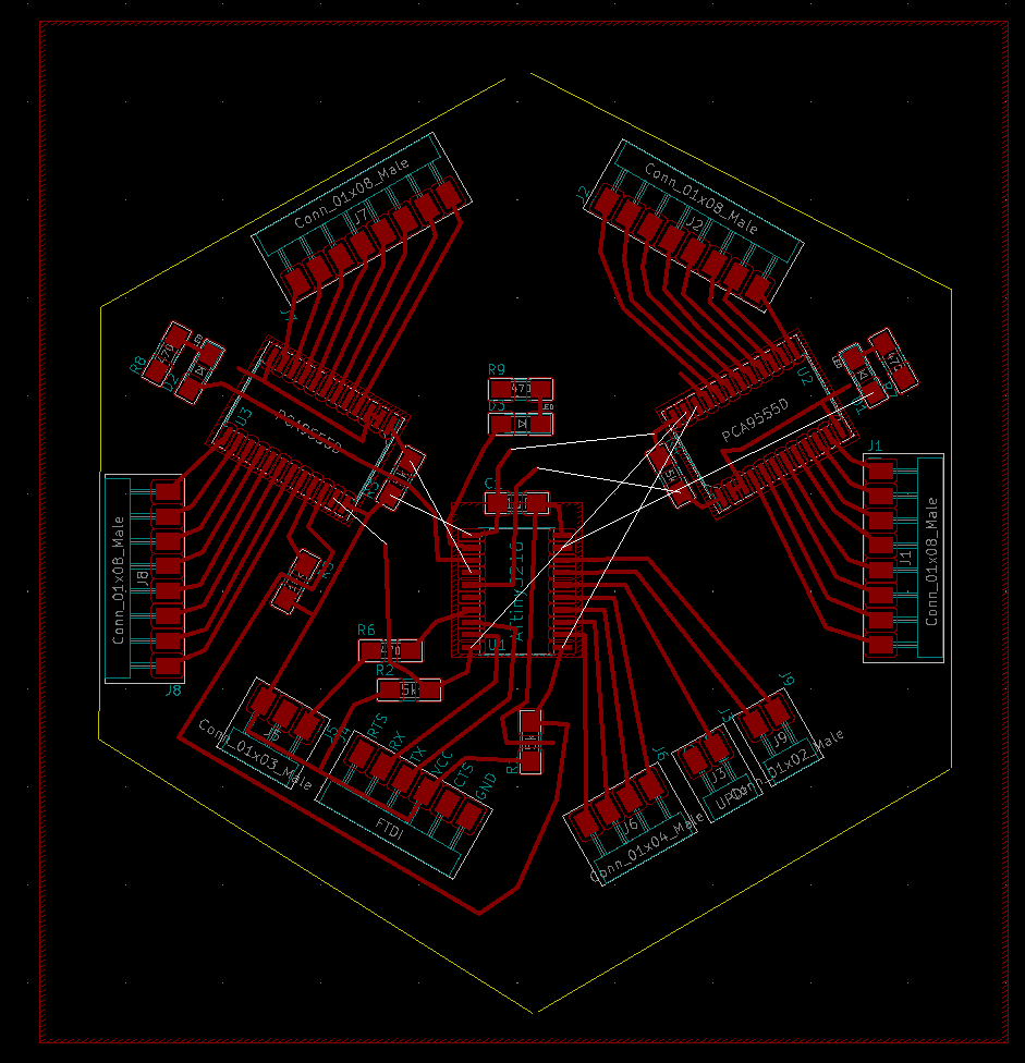

If one hexagon really wasn’t an option, I figured I might go for a more rectangular layout. Perhaps three smaller hexagons that were partly joined together; two for each of the PCA9555Ds and their components and one for the central ATtiny3216 and the remaining components.
That almost solved the size issue. However the second biggest issue that became a big hurdle; traces having to cross over each other. Each PCA9555D was basically connected to the ATtiny with 5 pins; 5V, GND, INT, SDA and SCL. However, the SDA and SCL pins on the ATtiny3216 are on opposite sides of the microcontroller, with the FTDI generally having to run its TX and RX line in between.
For the PCA9555D on the left, I saw that I could make the order of the traces running towards it in about the same order as the PCA9555D required it. However, for the one on the right, it therefore had to all be mirrored (since it was rotated 180°).
At one point I finally had a board that was functionally all connected, but it needed a whopping eight 0Ω bridges! (and it looked ridiculous).
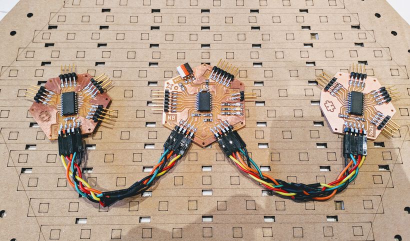
Taking a short break, I reassessed the board and decided on two big changes; I’d move my TX and RX pins to their alternate positions, so I didn’t have the TX and RX lines crossing in between the SDA and SLC lines anymore. Plus, I would separate into three boards, instead of trying to fit it all into one. There would be one bigger main board with the ATtiny3216, while each PCA9555D and their connector pins would get their own board.
Splitting the boards basically gave me access to more unofficial “bridges” because I could place wires behind the pin connectors of both boards. It still took me a long time to draw all the traces correctly and make it look nice. But finally around 10 in the evening I had the boards where I wanted them:
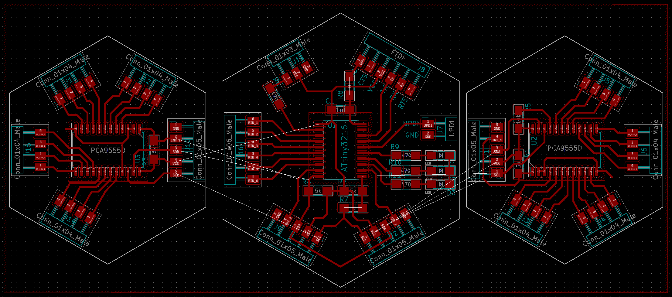
Because I essentially made three separate boards with one schematic, there are still some white lines in the image above (indicating missing traces). However, I knew these would eventually be fixed by connectors running between the main board and the two PCA9555D boards (I checked at least ten times if all was correct).
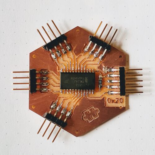
I added the (expected) I2C addresses of the two PCA9555D boards as text to the boards; 0x20 and 0x21, while also annotating many other connectors with labels so I would hopefully not mess up the connections.
I opened the traces PNG in Illustrator and made some final tweaks.
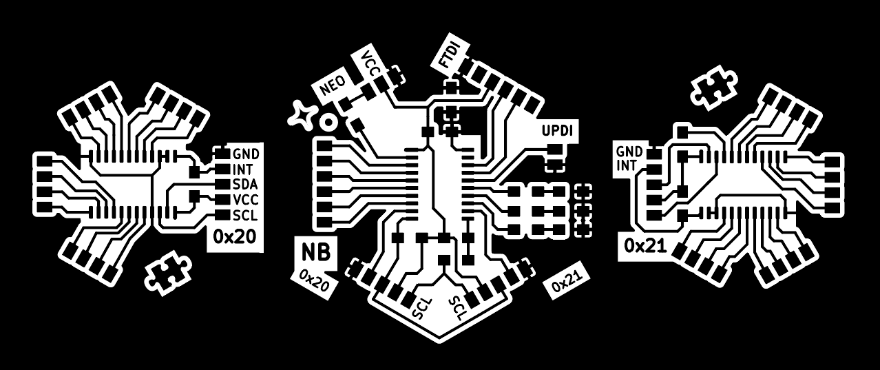
These three boards together were longer than the width of a copper plate. I therefore knew that I had to mill them separately. To make sure that I would keep the traces and interior aligned, I copied the interior SVG into the traces document. I then created three separate artboards (one for each PCB board), and using the File -> Export -> Export as option, I always check Use artboard, which saves all three artboards separately in one go.
The only thing I had to do is to make sure the correct layers were visible in Illustrator to first save the traces and next the interior.
I added some holes to the interiors of each board so I could use these to either fix the boards to the bottom of the NeoPixel plate, and to potentially solder some wires to for the GND connection of all the puzzle pieces.
Milling & Soldering the Board
I started to mill the main board first. All was going well with the traces, but while doing the interior the mill suddenly plunged into the copper (O_O) I stopped the process and Henk came to check. I looked at the outlines in mods, but it all looked good.
Then Henk moved the milling head up, but to my surprise the milling bit itself remained! The bit had apparently gotten loose! Ouch, bad mistake on my part. I guess I hadn’t screwed the grub screw in far enough (>_<) Thankfully, nothing bad had happened to the milling bit, the 8mm is quite sturdy, nor to my board. I reset the mill and made sure to tighten the milling bit really well.


Interestingly enough, the exact same happened to fellow student Loes who milled after me. During the milling of the trace of her board, the milling bit also came loose. That couldn’t be a coincidence. Loes investigated a little and noticed that the grub screw had a point where it seemed a little tight, but if you pushed on, you could actually tighten it even more. She “fixed” this by just screwing the grub screw in and out of the milling head a bunch of times until that “rough point” was eroded away.
Milling the second board went without any issues thankfully, except that the traces looked very thin. A quick check with the multimeter showed that they were still connected though.
On the third board I mixed up the size and used the width of the board to check if there still was enough height left on the copper plate to mill. I noticed my mistake while milling the outline and saw that the milling bit ran outside of the copper plate (°Д°) Sadly, my final board is thus missing the little tippy of of one corner (and missing one hole).

No traces were missing thankfully, but still, my perfectionist self is itching when I see it ✖_✖
The soldering of all three boards went well. No problems along the way. I used Phil’s tip with the Flux/Soldering Paste that I’d learned last week to solder on the central ATtiny3216 and PCA9555Ds; put some flux on each of the pads on the board and on the pins themselves, while holding the device in place on the board put some flux on the tip of the soldering iron and then touch it to a pin, and the solder is sucked from the tip and onto the trace + pin, flowing in place. Soldering those tiny pins has never been so easy, even if there’s no trace running outward (but moving under the device).


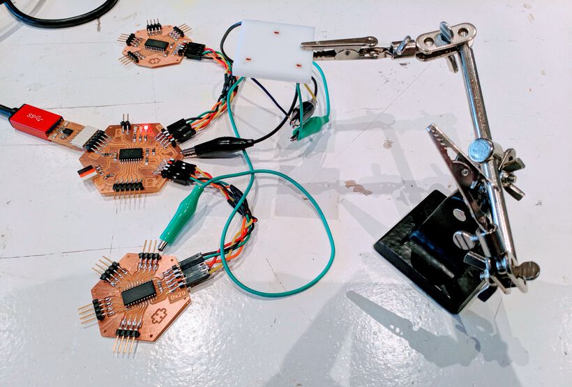
Programming My Boards
After checking that the three LEDs on my main board were working I grabbed five female-to-female jumper wires to connect the 0x20 PCA9555D board and see if I could make the connection to it.
Connecting to the PCA9555Ds
I found some example code to scan for I2C addresses on the Arduino website. I was wondering / hoping if I’d indeed get a result from the 0x20 address (otherwise I’d be a bummer since I’d had that address milled on onto the board itself (*^▽^*)ゞ
). Thankfully, after uploading the code to my main board the result was what I was hoping for:

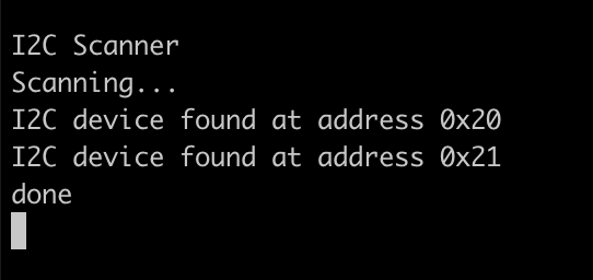
And the second PCA9555D board was thankfully also found at the expected address of 0x21 address after hooking it up to the main board as well.
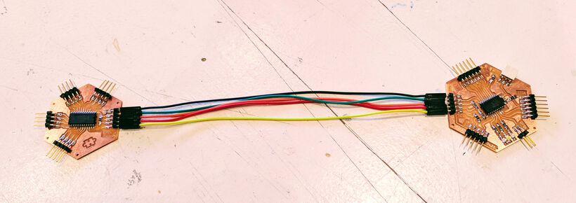
Those female-to-female wires were way too long though. I therefore tried to figure out how I would position the three boards on the cardboard NeoPixel prototype that I still had at the lab and thus how much I would need to shorten the wires.
Cutting, stripping, twisting, fluxing (the twisted tips), soldering, and adding a shrink tube on ten wires. For “cable management” I searched how to braid with 5 threads and breaded both sets of five wires from one end to the other (the shrink tubes were a bit to stiff for this though).
In my online search to understand the PCA9555D I had found an Arduino library specifically for the PCA9555D that made it possible to use function names that matched the typical Arduino language such as digitalRead.
I used a code example from Harm to get a feeling for working with the library, such as starting up the I2C connection and how to address the specific pins. Harm had been using all pins as output, while I only needed input pins. I therefore turned it into my own code that would switch from the red to the blue LED if the 0th pin of either PCA9555D board was “switched” (e.g. a connection to GND was made):
#include "clsPCA9555.h"
#include <Wire.h>

#define PIN_LED_RED 11
#define PIN_LED_BLUE 13

#define PIN_INT_0x20 7
#define PIN_INT_0x21 10

//Define the two boards and their addresses
PCA9555 board_0x20(0x20, PIN_INT_0x20); //16 GPIO pins
PCA9555 board_0x21(0x21, PIN_INT_0x21); //16 GPIO pins

void setup() {
  Serial.swap(1); //Use alternate TX/RX positions
  Serial.begin(9600);

  pinMode(PIN_LED_RED, OUTPUT);
  pinMode(PIN_LED_BLUE, OUTPUT);

  //Start I2C
  board_0x20.begin();
  board_0x21.begin();
  //Set the I2C clock to 400kHz (found in the datasheet)
  board_0x20.setClock(400000);
  board_0x21.setClock(400000);
  //Put all pins to input (pull-up)
  for (uint8_t i = 0; i <= 16; i++) {
    board_0x20.pinMode(i, INPUT);
    board_0x21.pinMode(i, INPUT);
  }//for i

}//void setup

void loop() {
  //Turn on the blue LED if a connection is found on pin 0
  if (board_0x20.digitalRead(0) == LOW or board_0x21.digitalRead(0) == LOW) {
    digitalWrite(PIN_LED_RED, LOW);
    digitalWrite(PIN_LED_BLUE, HIGH);
    Serial.println(0);
  } else {
    digitalWrite(PIN_LED_BLUE, LOW);
    digitalWrite(PIN_LED_RED, HIGH);
    Serial.println(1);
  }//else

}//void loop
Interestingly, while looking for more code examples of the PCA9555D I came across the forum post that led to the creation of the PCA9555D library (it’s in Dutch). Here is another example of code using that library.
I also found examples of being able to program the PCA9555D without the library, such as this one, this, and this one. However, the library just makes it so much easier. I did check the underlying code of the library to see what arguments each of the library’s function could take and what each function did.
I saw that there didn’t seem to be anything special to set an INPUT to an INPUT_PULLUP, but an online search told me that “The pull ups are always active if the pin is programmed as an input”, great!
I attached an alligator clip to the 0 pin of the 0x20 board and another to GND. I attached two stripped wires to the other side of the alligator clips and tested placing them against a copper piece, to mimic a puzzle piece landing on two small connection points:
I also checked the Serial monitor and didn’t see any debouncing of the “switch”, which showed me that the internal pullup resistor was indeed doing it’s job. But also, YAY, the PCA9555D board was working in general! (^ᗨ^)
Puzzle Contact Points
I wanted to create a “contact point” prototype that was more realistic to test. To better understand what I could truly use for the bottom plate of my puzzle.
My very first idea had been to mill out two circles from a piece of copper plate to function as the contact points inside the bottom plate of the puzzle and a small connection section that would go on the underside of each puzzle piece.
I made a quick mockup in Illustrator and had it milled:
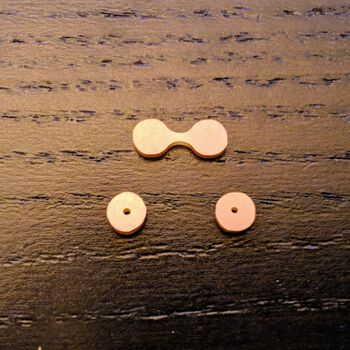
However, I started to realize that this had several downsides. For one, the milling machine was actually not that good at milling small circles. I’d noticed this already when I’d put circle marks on some of my previous boards, so the resulting pads were a bit crude. But that was a small issue though.
Another point was that these were about 5mm in diameter. I thought that was small at first, but seeing them I felt they looked huge, especially when considering that the bottom plate would get two for each puzzle piece, thus 56 in total. I could mill them smaller, but not super small, I needed that internal hole to solder a wire to that would carry the signal to the PCA9555D boards.
Finally, and this was the biggest issue, the copper plate had a thickness (obviously). That meant that I had to etch out a section from the acrylic bottom plate to the thickness of the copper plate exactly. Too deep and the copper circle would fall in too far and be unable to make contact. Too high and the puzzle piece on top would probably wobble. And I’d have to glue them into the puzzle board as well, could I control the extra thickness that the glue would introduce?
This all just felt like too many uncertainties and things having to go perfect to be a good solution.
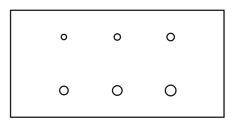
I therefore did a test using a much simpler idea; to create small holes in the acrylic and stick a partly stripped jumper wire through it, glueing it in place.
Using Cuttle I made a super simple and small rectangle of 10x20mm with holes of increasingly larger diameter; from 0.5 to 1mm:
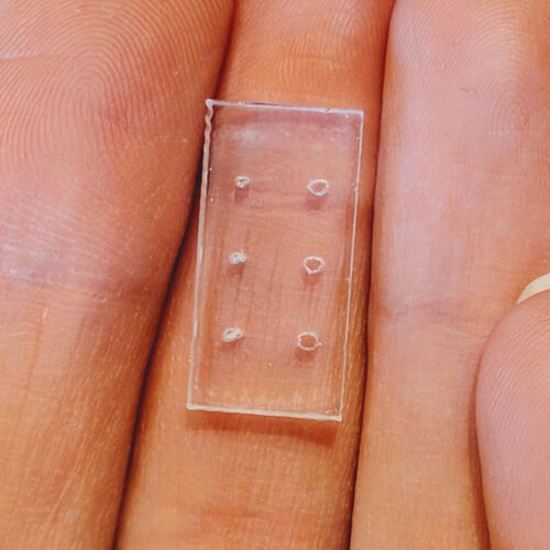
My first try in cutting it from acrylic failed though because I’d set the speed too high (40 speed & 80% max power), this resulted in circles that weren’t circular enough (see image above right).
Another test at speed 10 & max power 40% did result in good holes (I think the power can go down to 30% actually).
Some stripped wires of different sizes and materials and super glue later and I had a tiny, tiny prototype. I tried both sticking the wires out just enough, but it was generally easier to glue them in sticking far out and then cutting them short afterwards.

It was a little hard to cut them nicely though, and evenly, and the glue left some ugly marks on the acrylic. Nevertheless, when I placed a copper plate on top of the acrylic while two wires were connected to my boards, they did register.
Rivets as Contact Points
When Henk came to look at my clumsy progress he suggested to try and use copper rivets instead. These are generally used to connect the two sides of a double copper plate as a via. They are incredibly small!

The lab has three sizes, which give the internal diameter: 0.6, 0.8 and 1mm. Henk suggested to try and use the thinnest acrylic plate in the lab and see if I could set these rivets in them and then solder wires to the bottom of the rivet.
The thinnest plate that we could find was still ±1.8mm, which was about as thick as the rivets were long. Nevertheless, I made a quick update to the hole test, creating three rows with three sizes of holes, one row per rivet size, running from the outer diameter to 0.1mm and 0.2mm larger.
That showed that I’d need to go 0.1mm up from the outer diameter to make the rivets fit into the hole (I used a kerf of 0.1mm).
Henk then showed me how to use the rivet machine that would flatten the other side of the rivet. You place two heads inside a large “press”-like machine; you screw in the top being very careful not to let it drop, afterwards you can plug in the bottom side.


Next, you place the rivet into the tiny circle of the head, and starting pressing the large handle to move the rivet head down.
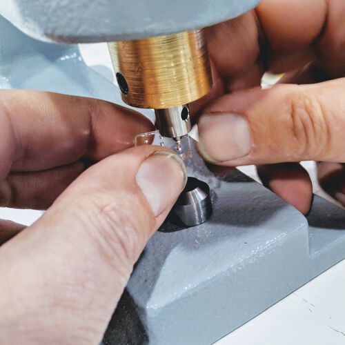
Once the two sides meet up you apply a little more pressure (don’t hit the handle, just push) and the rivet will be squished and flattened on the other side.
Or, well, that will happen with thinner materials. With this somewhat thicker acrylic plate nothing much happened except that the rivet seemed a little more stuck.
Stuck enough at least to try and solder some stripped wires to the underside. I put a glob of flux on the underside and wire, held both in place with a third hand and came in with a soldering iron and some solder. And it actually worked, I could solder the wires to the rivets. Except for the 0.6mm rivets, I couldn’t get the wires to enter those holes.

It also worked when I did the “connection test” with my boards.
This method had the bonus of always resulting in the same little height in “bump” sticking from the top of the acrylic layer. And although the diameter of the rivets were bigger than simply a wire, it didn’t look that bad because they were nice looking copper circles.
I was noticing that even though the rivets were barely sticking out from the top of the acrylic, the puzzle piece was wobbling on top of them. Back at home I talked it over with my partner and he said that you need three contact points to stop a wobble. He explained to me that, ideally, you want to create a triangle shape with those three points, as large as the puzzle shape can handle, where all the sides are equally long, and finally, the center of gravity should be lie somewhere within the triangle.
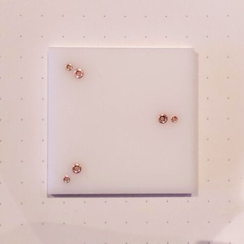
Back in the lab the next morning I therefore created yet another quick test in Cuttle; a square that was about the size of my “prototype” puzzle piece (that I’d cut out of acrylic a few weeks ago), and added three holes; three for the 1mm rivet and 3 for th 0.8mm rivet.
I took some (used) acrylic that still had space for a 35x35mm square and that was about the thickness that I wanted for my actual puzzle bottom. I made sure to set the speed to 10 (power to 40%).
It took quite some fiddling to get the ultra tiny rivets into the holes though (*≧▽≦)
I stripped some wires to solder to the rivets. However, I couldn’t get the solder deep enough into the hole to connect the wire to the rivet, with the acrylic sheet being about 3mm thick instead of the 1.8mm I tested with the day before.
That meant that I had to somehow prepare the rivets + soldered wires through some other means and then string them through the holes in the puzzle bottom plate. That meant that the 0.8mm rivets were out, the hole was too small for a jumper wire to pass through. Thankfully, it did just fit through the hole for the 1mm rivet!
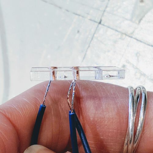
I made some updates to the “hole test” rectangle to make one with 9 holes all of 1.5mm in diameter. I cut this from the thin acrylic sheet. I then plugged some rivets in there and using flux, I soldered a wire to the end of it. I could then pull the rivet + wire out and loop it into the white thick acrylic sheet.

I took some copper tape and added it to one side of my “prototype” puzzle piece to act as the bridge between two contact points in the white acrylic sheet.

I then set the white square with three connection point into a third hand, connected two of wires to my boards, and watched what happened when I placed the puzzle piece onto the sheet:
There was some slight debouncing as I first placed the piece or took it away, so I’d probably have to work with some timing function in my code (i.e. only do X if the pin has been “activated” for at least X milliseconds), but that was a minor thing.
Helping Others With I2C
Because the PCA9555D library made working with I2C so easy I wanted to mention that I have come into contact to working with the standard I2C library, Wire, while I was helping fellow students Nicole, Phil, and Loes (on separate points in time).
All three had created separate boards, each with their own ATtiny on them, not a device like the PCA9555D that had the I2C address basically built into it.
Nicole was the first one I helped. She couldn’t seem to make contact between her boards. The Serial Monitor seemed to indicate that nothing was ever received by the “baby board”. In the end I think it was due to the address setting? Although I’m not 100% sure if that was all. Nevertheless, after we switched from using an address such as 9 to 0x09 the baby board was picking up messages. Almost all the online examples that I came across while trying to debug used things such as 9 though, but those were all Arduino’s. Perhaps the Attiny’s required an actual hexadecimal code?
Although I don’t have the code that finally worked for Nicole, I think it was the following:
//Manager code
#include <Wire.h>
int x = 0;

void setup() {
  //Start the I2C Bus as Manager
  Wire.begin();
}//void setup

void loop() {
  Wire.beginTransmission(0x08); // transmit to device 0x08
  Wire.write(x);                // sends x
  Wire.endTransmission();       // stop transmitting
  x = (x+1)%6;                  // cycle x through 0 - 5
  delay(500);
}//void loop
//Staff code
#include <Wire.h>
#define LED 13;
int x = 0;

void setup() {
  Serial.begin(9600);
  pinMode (LED, OUTPUT);

  //Start the I2C Bus as Slave on address 0x08
  Wire.begin(0x08);
  //Attach a function to trigger when something is received
  Wire.onReceive(receiveEvent);
}//void setup

void receiveEvent(int bytes) {
  while(Wire.available() > 0) {
    x = Wire.read();    // read one character from the I2C
    Serial.println(x);
  };
}//void receiveEvent

void loop() {
  //Turn on the LED
  digitalWrite(LED, HIGH);

  //If value received is 0, turn off LED
  if (x == 0) {
    digitalWrite(LED, LOW);
    delay(500);
  }//if
}//void loop
Which came from this tutorial mostly.
With Phil the code just completely froze after running Wire.endTransmission(). After some googling, and a close inspection of his board, I noticed that his SDA and SCL resistors said 4999, while I remembered that mine said 4991. He’s accidentally soldered on 49.9Ω resistors instead of 4.9kΩ. Apparently he’d used resistors that were lying loose in the 4.9k box, and someone had put in 49.9 in the 4.9k box 눈_눈
With the bigger resistors in place, the code functioned properly!
And finally, with Loes, she had the issue that the I2C scanner was returning no found addresses. I explained that she had to first give her baby boards an address before the I2C scanner would find anything, by including #include <Wire.h> at the top of her baby boards and then adding Wire.begin(0x08); to the setup function, where each baby board got a different address.
Sadly, while making these changes she experienced a short circuit on her mama board which was dead afterwards, and she could not check if my suggestion was the solution.
Bonus | A Table Light - Part 2
During the previous week I explained how I’d bought a 12V LED strip for the large ceiling light that I created during the “Computer-Controlled Machining” week, where I used an ESP32 Dev board to create (hardware) PWM to dim the light.
Since we’re now in the Networking week, I wanted to explain the next step; being able to control the brightness through a website, and eventually with the Google Home app and voice activation.
Setting Brightness Via A Website
I started with examples on how to create a web server. Although there were several examples to be found online, I was (and still am) confused by the different ways that people went about it. Some used WiFiServer server(80), others WebServer server(80), and yet others went with AsyncWebServer server(80), each with their own libraries.
I generally try and start with en example that seems the simplest, which in this case was this snippet that checks the current state of “something” and then prints it on the website that is created by the ESP32.
I didn’t copy everything, just the part that would start the server and print out the IP address:
I then copied the code from this page, which uses WebServer instead, primarily because it was short and used some simple HTML and styling within its code to style the website. Nothing mayor, but I just wanted to get a sense of how it could work.

Now that I had a webserver running and could change the text on the page, I wanted to know how I could change things using buttons, sliders, forms, etc. through the webpage and then see the ESP32 capture that change.
While searching for examples about being able to control a simple LED with the ESP32 web server I came across a tutorial from RandomNerdTutorials that used AsyncWebServer server to input a value into a form, and having the ESP tell you what value it was:
#include <WiFi.h>
#include <AsyncTCP.h>
#include <ESPAsyncWebServer.h>

AsyncWebServer server(80);

// REPLACE WITH YOUR NETWORK CREDENTIALS
const char* ssid = "REPLACE_WITH_YOUR_SSID";
const char* password = "REPLACE_WITH_YOUR_PASSWORD";

const char* PARAM_INPUT = "input1";

// HTML web page to handle an input field
const char index_html[] PROGMEM = R"rawliteral(
<!DOCTYPE HTML><html><head>
  <title>ESP Input Form</title>
  <meta name="viewport" content="width=device-width, initial-scale=1">
  </head><body>
  <form action="/get">
    input1: <input type="text" name="input1">
    <input type="submit" value="Submit">
  </form>
</body></html>)rawliteral";

void setup() {
  Serial.begin(115200);
  WiFi.mode(WIFI_STA);
  WiFi.begin(ssid, password);
  if (WiFi.waitForConnectResult() != WL_CONNECTED) {
    Serial.println("WiFi Failed!");
    return;
  }
  Serial.println();
  Serial.print("IP Address: ");
  Serial.println(WiFi.localIP());

  // Send web page with input fields to client
  server.on("/", HTTP_GET, [](AsyncWebServerRequest *request){
    request->send_P(200, "text/html", index_html);
  });//server on

  // Send a GET request to <ESP_IP>/get?input1=<inputMessage>
  server.on("/get", HTTP_GET, [] (AsyncWebServerRequest *request) {
    String inputMessage;
    String inputParam;
    // GET input1 value on <ESP_IP>/get?input1=<inputMessage>
    if (request->hasParam(PARAM_INPUT)) {
      inputMessage = request->getParam(PARAM_INPUT)->value();
      inputParam = PARAM_INPUT;
    } else {
      inputMessage = "No message sent";
      inputParam = "none";
    }
    Serial.println(inputMessage);
    request->send(200, "text/html",
        "HTTP GET request sent to your ESP on input field ("
        + inputParam + ") with value: " + inputMessage +
        "<br><a href=\"/\">Return to Home Page</a>");
  });//server on

  server.begin();
}//void setup

void loop() {
}
I was surprised that it was all handled within the setup function of the code, while the loop remains empty. I think what happens is that the ESP sets up the web server when it gets power. It then has two .on event handlers that are attached to the web server that will run, and only run, whenever there is a request on the main IP address (the first .on handler), or when you are routed to the /get subdomain after filling in the input field (the second .on handler) from which you can read the value that was input. That way it’s only really doing anything when the website is visited.
I also saw that the HTML of the ESP32’s site was contained as code within a const char index_html[] PROGMEM = R"rawliteral(<!DOCTYPE HTML><html>...</html>)rawliteral";. I don’t understand the PROGMEM or R"rawliteral, however I understood the code/HTML within it.
Having this piece of code working, and seeing the number returned I wove the ledcSetup/ledcAttach, and ledcWrite throughout the setup function to be able to attach the number that was returned from the website to the duty cycle of the PWM signal (what I worked on last week).
I adjusted the if statement of the server.on("/get",...) statement to:
if (request->hasParam(PARAM_INPUT)) {
  inputMessage = request->getParam(PARAM_INPUT)->value();
  //Turn the character value into a float
  value = inputMessage.toFloat();
  Serial.print("Value entered: ");
  Serial.println(value);

  if(brightness >= 0 && brightness <= 100) {
    // Map from 0%-100% value to 0-MAX_DUTY_CYCLE value
    brightness = map(brightness, 0, 100, 0, MAX_DUTY_CYCLE);
  } else if (brightness > 100) {
    brightness = MAX_DUTY_CYCLE;
  } else {
    brightness = 0;
  }//else

  //Set the PWM duty cycle
  ledcWrite(PWM_channel, brightness);

}//if
And it worked! I could input a value into the website, and the ESP32 would print it out on my Serial monitor ʕ•ᴥ•ʔ
What happens is that when you’ve entered something into the input field and pressed ENTER, the page directs you to a subdomain with a URL of <<IP Adress>>/get?input1=<<value input>>. The second server.on handler will be called when you go to the /get domain. It will get the full URL of that page, including everything after the ?. It then checks if a certain parameter is present in the full URL, which was called "input1" here with request->hasParam(PARAM_INPUT). If the parameter is present it will then request the value given to that parameter, the part after the = with request->getParam(PARAM_INPUT)->value(); Finally, I turn that string into a float variable with the .toFloat() function, which is used to set the brightness of the PWM signal.
However, instead of an input field I wanted to create a range slider, feeling more true to how you can change the brightness of lights in the Google home app. Thankfully, RandomNerdTutorials also had a tutorial showing exactly that. I really should’ve found this tutorial sooner, it was basically all I needed, even having incorporated the ledc functions as well (*^▽^*)ゞ
I copied the relevant parts over into my code. However I wasn’t keen on the yellow-black rectangular slider styling they’d created and therefore adjusted the HTML section within the rawliteral to:
// HTML web page to handle the range slider
<!DOCTYPE HTML><html>
  <head>
    <meta content="text/html;charset=utf-8" http-equiv="Content-Type">
    <meta content="utf-8" http-equiv="encoding">
    <meta name="viewport" content="width=device-width, initial-scale=1">
    <title>ESP32 LED Lamp - Adjust brightness</title>
    <style>
      html {font-family: monospace; text-align: center;}
      h2 {font-size: 2.3rem;}
      p {font-size: 1.9rem;}
      body {margin:0px auto;}
      .slider {width: 360px; height: 4px; background: #9ea1a1;}
      .slider::-webkit-slider-thumb, .slider::-moz-range-thumb {
        width: 22px;
        height: 22px;
        background: #27c9e3;
        border-radius: 14px;
        border: solid black 3px;
      }
    </style>
  </head>
  <body>
    <h2>ESP32 LED Lamp - Adjust brightness</h2>
    <p><span id="brightnessSlider">%SLIDERVALUE%</span></p>
    <p><input class="slider" type="range" onchange="updateSliderPWM(this)" id="pwmSlider" min="0" max="1" value="%SLIDERVALUE%" step="0.01"></p>
    <script>
    function updateSliderPWM(element) {
      var sliderValue = document.getElementById("pwmSlider").value;
      document.getElementById("brightnessSlider").innerHTML = sliderValue;
      console.log(sliderValue);
      var xhr = new XMLHttpRequest();
      xhr.open("GET", "/brightness?value="+sliderValue, true);
      xhr.send();
    }
    </script>
  </body>
</html>
To really test it, I added the ESP32 and a blue LED to a breadboard, connecting them to use PWM to set the LEDs brightness.
I was super excited when I saw that moving the slider on my screen would adjust the brightness of the LED (๑•̀ㅂ•́)ง✧
Setting Brightness Using Voice
Although handy for the website, this wouldn’t be handy for me to use for the ceiling light; first having to navigate to the page to set its brightness. Thankfully, you can bypass the whole website “experience” by going straight to the URL that calls the second server.on handler that gets the brightness value. I simply go straight to <<IP address>>/brightness?value=50 and the ESP32 will read the value 50 and use it for the brightness.
Using this I could start on my final step; hooking the light up to Google Home. Thankfully, my partner is very interested in domotica and automating our house. We therefore already have a few Google Home speakers. More importantly, we have a Homey, which acts as a hub for all our smart devices, such as many of our lights, our CO2 sensor, Roomba, ventilation, etc. They are all connected as devices within Homey, which then serves them to our Google Home for easy access.
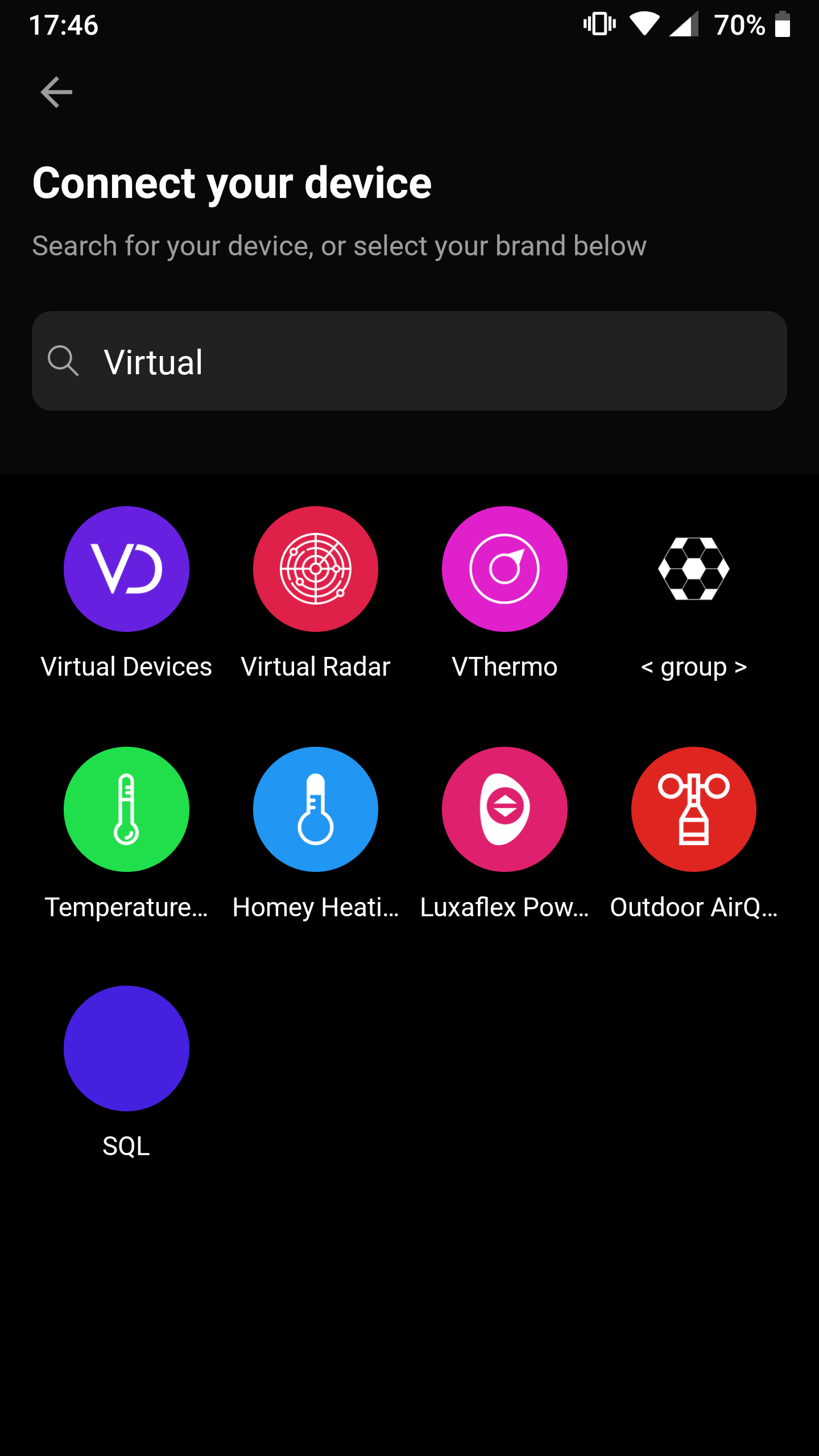
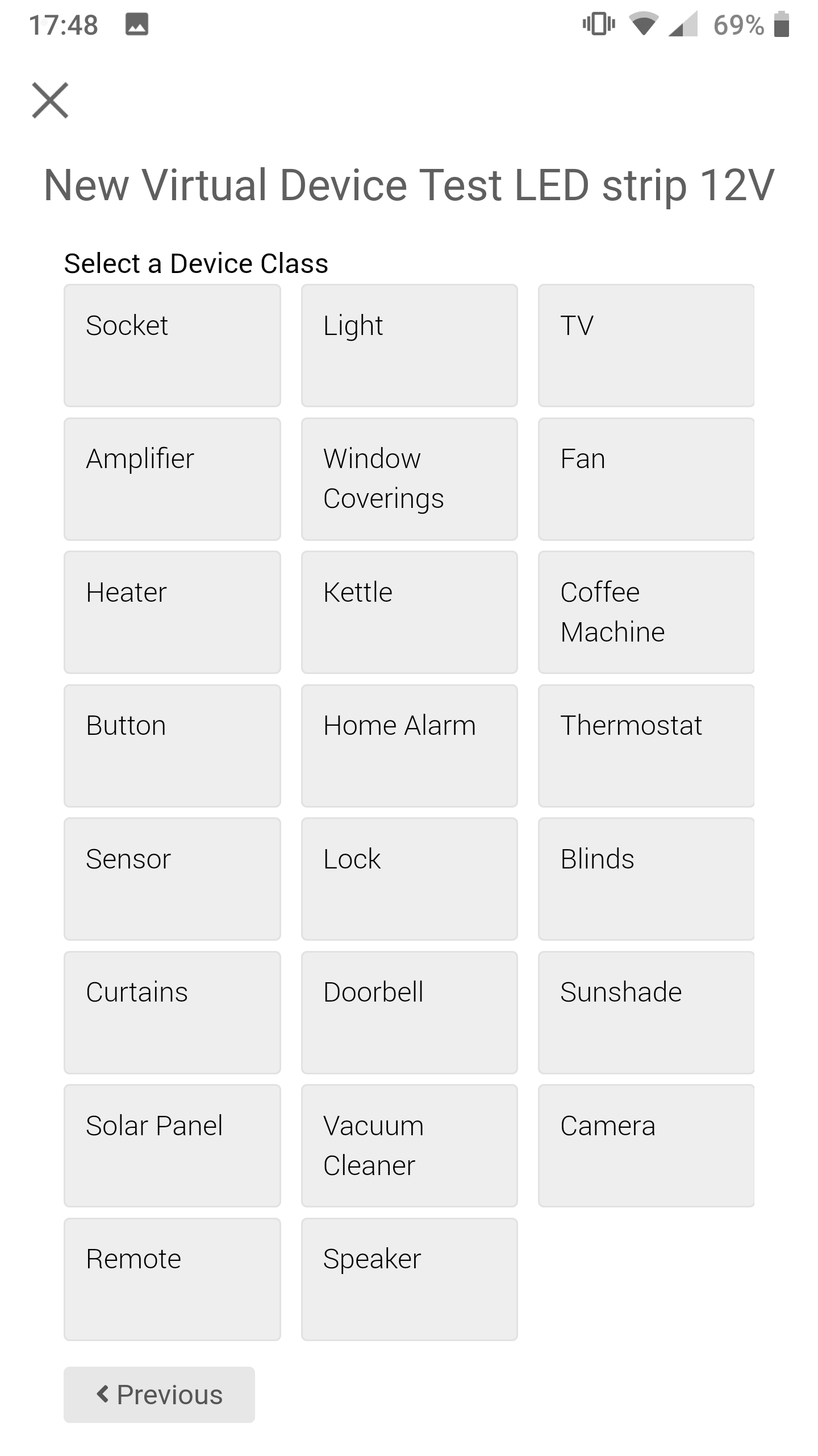
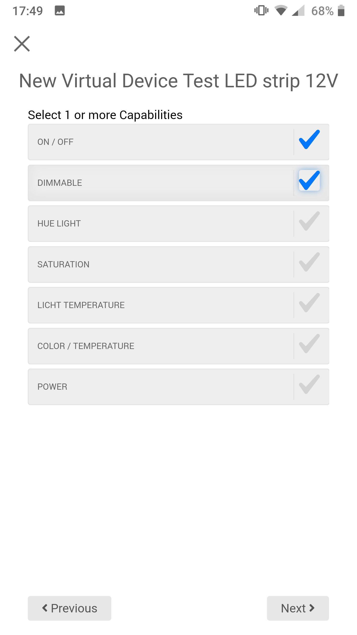
Within the Homey app I started to create a new device, a Virtual Device to be exact. In the next window, choose Device and follow the next steps to set its name, icon, and, very important, is the Device Class. This will determine what “functionality” Homey will give this virtual device. I choose Light, which will then ask you what options this virtual light should have, where I choose On/Off and Dimmable. Now that the virtual device is ready, the methods to turn it on and off and set its brightness in both the Homey and Google Home app will look like as if I’d added an actual smart light to our home.

For now I had a virtual light. However, it’s not connected to my ESP32. What I needed to happen was:
- If I turn the light on in either the Homey or Google Home app, it needs to go to
<<IP address>>/brightness?value=<<last brightness level>> - If I turn the light off in either the Homey or Google Home app, it needs to go to
<<IP address>>/brightness?value=0 - If I adjust the brightness slider in either the Homey or Google Home app, it needs to go to
<<IP address>>/brightness?value=<<brightness level>>
Thankfully, the virtual light in Homey has a variable called dim level associated with it. This automatically remembers the last brightness that was set using dimming (so not using an ON or OFF).
I won’t go deeply into this, but one of the fundamental aspects of Homey is to be able to set flows. This lets you truly automate devices, such as setting the warmth of all smart lights in your home based on if the Sun is up or not (and smoothly changing from warm white to cool white during sunset/sunrise).
Using flows was also the way for me to attach an action to when I would use the ON, OFF, or brightness slider in the Google Home app. For example, if the variable dim level from my virtual lamp is changed (either through the Google Home or Homey app itself), it will start a flow. There are many many things that can happen within a flow, and a HTTP GET request is one of them; it will “get” that URL supplied, being the ESP32s web server, supplying the new dim level:
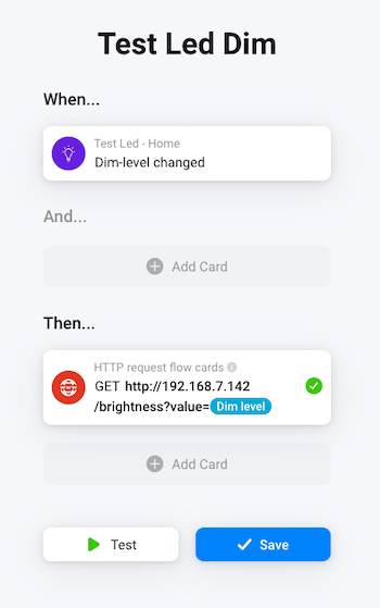
I created two more flows, one that should happen when the Test LED light is turned ON, making a GET request with exactly the same URL as the dimming (so it returns to the previous set dim level) and another one for turning the OFF, which has a GET request to.../brightness?value=0.
With it working in Google Home, it meant that voice control was an immediate bonus, as you can hear in the video below where I’m updating the brightness of the LED by talking to my Google Assistant:
Cool right!!! (ノ◕ヮ◕)ノ*:・゚✧ I actually hadn’t expected to be able to get here when I started playing with the LED strip. Admittingly, without the Homey going from the website to operating the lamp via an app would’ve probably been painful.
Cleaning Up Some Wires
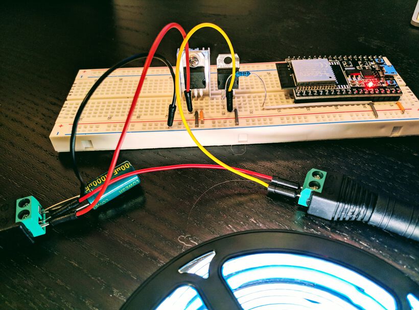
The above video is still using a simple LED. To bring this back to the actual 12V LED strip I had purchased a few electronic components after having figuring out the required circuit last week;
- A female and male 5.5mm jack plug to be able to add wires and the ESP32 in between the 12V power adapter and the LED strip.
- A 1000 μF capacitor to connect to the 12V power supply to protect the LED strip from the onrush of power.
- A L7805CV 5V voltage regulator and a heat sink to screw to its back. This can handle up to 35V as an INPUT voltage and outputs 5V on its OUTPUT pin, which I send into the ESP32 dev board.
I used my larger breadboard to place the ESP32, the transistor, and the voltage regulator side by side, using some small solderless breadboard wires on the board itself and a few jumper wires going to the power adapter and LED connection and voilà, both the LED strip and the ESP32 board were now powered through the 12V power adapter:
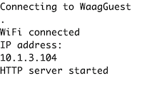
I then experienced some issues with the ESP32 seemingly not being able to create its web server. Strange, the red built-in LED on the board was on. Perhaps the IP address had changed? Although I’d asked my partner to fix the IP address of the ESP32.
I unplugged the ESP32 from the 12V power supply and connected it to my laptop via the USB connection. It worked then, and it was indeed still the same IP address as before.
I disconnected the USB cable again, however, this time I used jumper wires on the legs of the ESP32 dev board to power it from the 12V supply again. Simultaneously I also connected the TX connection of a USB-to-TTL to the TX of the ESP32 (and also the GND of both), so I could still see any messages coming in from the ESP32 while not supplying power at the same time. In this configuration the ESP32 was also setting up its web server without issues.
I disconnected all the jumper wires from the ESP32 again, not knowing what the issue could be. I pressed it back into the breadboard, and as I did, and unconsciously pressed a little harder I noticed that the onboard red LED shone brighter as I pressed down. Really? That was it? Gosh, my crappy longer breadboard was apparently not holding onto the ESP32 dev board well enough ✖‿✖ I pressed down the ESP32 into the breadboard with quite some force and finally it went and stayed in far enough, and sure enough, the web server was working.
Below you can see it working using the Google Home app (the brightness changes don’t seem that different, but that’s just my crappy camera):
Henk had advised me to create my own board using an ESP-01 (which has an ESP8266) for the WiFi connected to an ATtiny412 for the (hardware) PWM to have a smaller package. I spend an afternoon and evening trying to investigate how I could possibly go about this. However, just being able to program the ESP-01 itself was already quite a hurdle with having to connect some of its pins during programming, needing some reset button, disconnecting some wires again for normal usage. Furthermore, to connect it to the ATtiny412 you’d need to use the TX and RX lines, which if I’ve understood it correctly, also need switches if you want to reprogram the ESP-01 at a later stage.
All in all, after a few hours of research I was only full of frustration from not understanding well enough what should happen, how to bring it all together, and more. Continuing down this path would not be fun for me anymore, and I was too busy (and in all honesty, stressed) with the “normal” weekly tasks of Fab Academy to handle more frustration. I therefore decided to be ok with using a bigger pre-made dev board, even though it was overkill and I was only using 1 of its GPIO pins.
I did purchase a smaller ESP32 dev board, the D1 Mini that has the ESP32-WROOM-32, plus some prototyping PCBs onto which I’ll be soldering all the components. We purchased a small 12V/2A adapter, some nice looking power cables, and I designed and 3D printed a small “box” in which to place the adapter and the “soldered board”, which is attached to the ceiling right above the lamp. So, we’re actually getting close to having our light above the table! (well, I still need to paint all the wooden slices though (*^▽^*)ゞ ).
Reflections
Not a very of exciting result this week; an LED that lights up if a connection is made from a pin to GND (*^▽^*)ゞ , but this was all mostly in preparation for my final project, so I hope I’ll be able to create my actual puzzle bottom plate and solder all the wires to it and my boards pretty soon.
What went wrong
One milling bit came loose! I’d not tightened the 0.8mm milling bit well enough and it came loose and buries itself into the copper plate while milling the interior. Thankfully, nothing broke or was damaged, pfew!
I also have one board with a missing section because I’d used the width to see if there was just enough height left on the copper plate ( ̄ー ̄)
What went well
I think I figured out the PCA9555D well enough beforehand, so I could properly include it in my KiCad schematic (e.g. giving both a different address), so this time I actually didn’t have to make any changes to my board after the first soldering pass!
The programming also went without any issues. Partly thanks to the PCA9555D library that makes it very straightforward to work with, but also because I’ve not programmed anything difficult this week; that will come once I’ll be hooking up all the 38 puzzle piece connection points.
What I would do differently
I do wonder if using Male connectors for everything was the best option. There are no Female connectors in 01x04 or 01x05 sadly, otherwise I’d gone for those. And I only learned about those upright 02x04/02x06 options when I came to the lab on Monday, and I did not want to mess with my board design anymore, because I’d already taken way too long.
Wrapping up
At the start of this week I had a small hope that I could’ve created the full puzzle bottom plate this week, but it turned out to take more time to prototype the connection points and create the three boards. Soldering wires to all of the rivets will take a lot of time, but I’m happy that I now at least have a clear vision of how to continue with that bottom plate. Hopefully I’ll get to it next week!