6. Electronics design
Amsterdam, March 4, 2020
To do
| Description | status |
|---|---|
| Group assignment: use the test equipment in your lab to observe the operation of a microcontroller circuit board | done |
| Document my part of the group assignment | done |
| Redraw an echo-hello board. Add at least a button and a LED | done |
| Learn to use KiCad to design a PCB | done |
| Mill the PCB | done |
| Solder the PCB | done |
| Test the PCB | done |
| program the PCB | done |
| Document my individual assignment | ongoing… |
| Work on final assignment |
Source files
| Description | link |
|---|---|
| Echo board traces | Downloadable PNG |
| Echo board cuts | Downloadable PNG. |
| KiCad files (without the fp-info-cache file because too large) | Downloadable zip. |
| Freerouter files: .DSN file exported from Kicad .SES file exported from Freerouter | Downloadable zip. |
| Blink.ino file for programming the board with Arduino | Downloadable zip. |
urls
| Description | link |
|---|---|
| Index of this week’s topic | http://academy.cba.mit.edu/classes/electronics_design/index.html |
| Global lecture video | https://vimeo.com/395859588 |
| Global review video | https://vimeo.com/397463447 |
| Group assignment documentation | http://fabacademy.org/2020/labs/waag/groupAssignments/week6.html |
| Link to standard inventory FabLabs | https://docs.google.com/spreadsheets/d/1U-jcBWOJEjBT5A0N84IUubtcHKMEMtndQPLCkZCkVsU/edit#gid=0 |
This week’s outcome
Introduction to electronics
In the local lecture Henk gave us an introduction into electronics. He used a slide show that he shared with us over Slack. I will use this slide show to write down the take aways of his introduction to electronics.
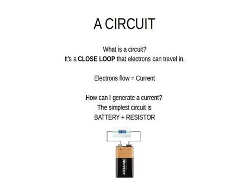
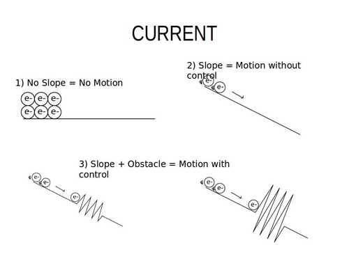
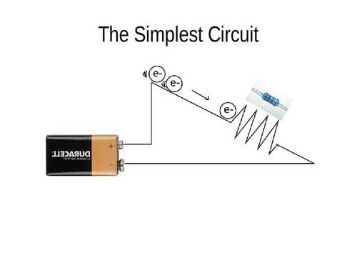
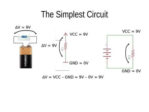
A circuit is a closed loop that electrons travel through. You need to put in a resistor to form an obstacle for the electrons. Otherwise they will run from VCC to GND and your battery will be empty in no time.
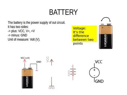
I looked up some extra information about voltage. Quoting from Fluke.com ‘Voltage provided by an energy source such as a battery is what causes current to flow. Voltage is the pressure from an electrical circuit’s power source that pushes charged electrons (current) through a conducting loop, enabling them to do work such as illuminating a light. In electricity’s early days, voltage was known as electromotive force (emf). This is why in equations such as Ohm’s Law, voltage is represented by the symbol E.
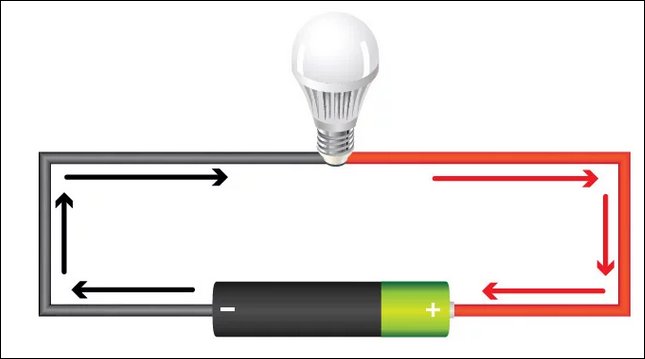 Image source: Fluke.com.
Continuing to quote from the Fluke.come source:
- In this dc circuit, the switch is closed (turned ON).
- Voltage in the power source —the “potential difference” between the battery’s two poles— is activated, creating pressure that forces electrons to flow as current out the battery’s negative terminal. (I would think it flows from the positive terminal. TR. The slide show also states that current flows from VCC to GND. I looked it up: appearantly there are two ways of looking at it: “That is actually a good question and discussed a lot. In the 1880’s especially. What is actually flowing is ELECTRONS, which are little negative charged particles. They are attracted by positive voltages. So ELECTRONS flow from “Ground” to “VCC” on an Arduino. This is “Electron Flow”. BUT the OldSkool “Conventional Current Flow” assumes current (whatever THAT is) flows from Plus to Minus. Source Arduino forum.
- Current reaches the lamp, causing it to glow.
- Current returns to the power source.
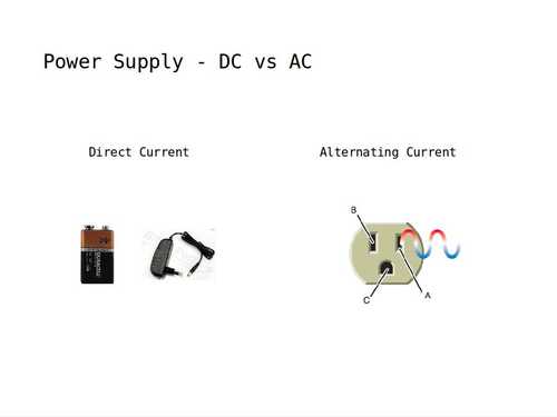
AC versus DC. Alternating current flows back and forth. DC goes one direction from VCC to GND. You house’s power outlet provides AC. Most electronic equipment works with DC. AC is converted to DC. The block on your laptop’s charger converts AC to DC.
AC symbol:  . DC symbol:
  .
.
You can measure voltage with a multimeter. Other things you can measure are: shorts, resistance, capicitance and temperature.
 .
.
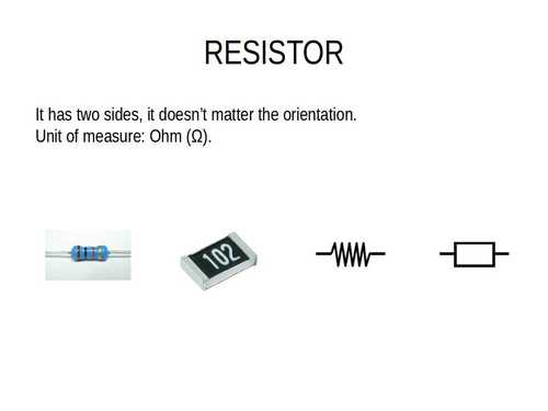
Resistors must be placed in any circuit to keep the electrons from spilling out incontrollably. A resistor works as an obstacle. In a circuit with only VCC and GND electrons display motion. The battery will quickly be empty. A circuit with a resistor is: motion of elektrons + control through the resistor. Resistors have no orientation. Some components must have a resistor to be able to work, for instance LEDs.
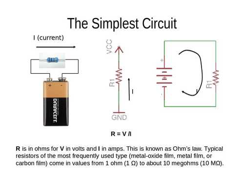
Ohm’s law I = V/R. Amparage is Volt divided by Ohms.
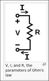
Source: Wikipedia
The current is the flow of electrons.
 Depicting current in a circuit.
 Voltage in a simple circuit.
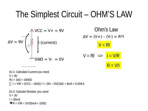
Ohm’s law. I = V/R. Can be used to calculate one of three variables when you know the other two.

Power is measured in Watt. P = VI (Power equals voltage times Ampare)
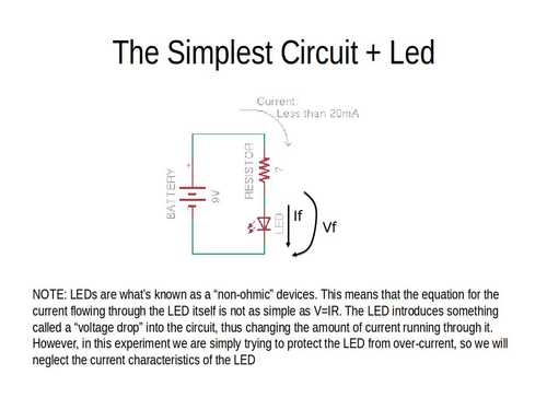
If you add a LED to your circuit you need to add a Resistor. A LED is a Diode and these are non-ohmic. That means they do not resist electrons, therefore they need a resistor. Look up in the datasheet how much current it can handle and calculate the resistor. You must protect it against over-current. The resistor can be placed before or behind the LED.
In the datasheet you will see voltage/current forward. That is the maximum current the LED can handle.
Also mind the minimum voltage it needs to light up. For instance a 1.8V LED needs that amount of voltage to light up. There are LED calculators available online to make these calculations.
All the components we use are 1206. This is about the footprint of the component, the type of packaging. It states the size and 1206 is a size that can still be soldered by hand.
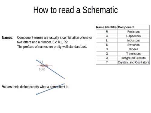
A schematic is the symbolic representation of an electronic circuit.
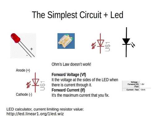
The symbolic representation of a LED. It has a + and a - side. Thus LEDs have orientation. The + side is called an Anode, the - the Cathode. Current flows from VCC to GND, so place your LED with its Cathode toward VCC and its Anode towards GND. It does not matter if you place the Resistor before or after the LED (I think).
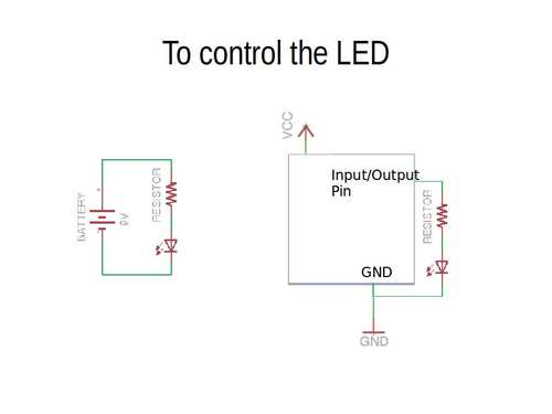
So now you have a LED but you want to make it blink. Connect it to a pin of the chip. Program the chip, communicate through the pin to the LED. Tell it to bLiNk.
In this image you see three parts of the steps of making an electronics board. First you make a symbolic schematic. Then you draw the board by placing it’s components and drawing traces between them. Then you mill the board and solder the components on it.
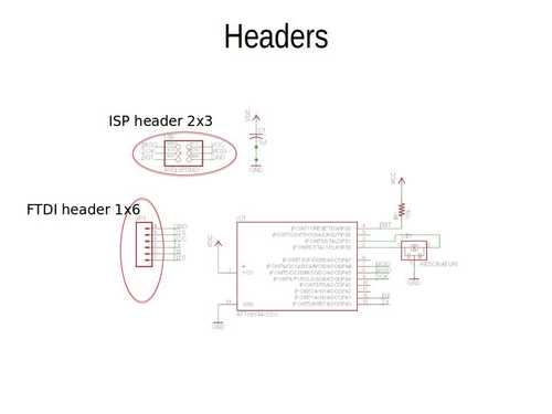
Headers. Headers are a means to connect a cable to your board for communication to other devices. The headers as a component have no orientation. The pins are ‘neutral’. They are just solid wires that conduct current. Once the header is placed on the board it does have orientation as each of the pins is now connected to other components of the board and transmit the information of that component. So how you orient your cable on the pin header is relevant.
Headers can have an x amount of pins. Pins are organized in rows. For instance: You can have 1 row of 6 pin or 2 rows of 3 pins. Represented as 1x6 and 2x3 respectively.
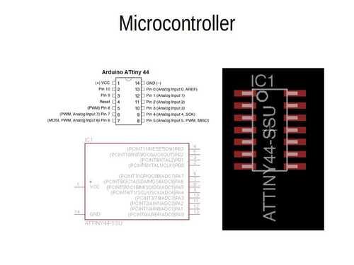
Microcontrollers run the computations. That is to say: current runs through them flipping transistors on and off. The 1s and 0s of machine code determine whether a transistor is on or off. A combination of millions of transistors all in either 1 or 0 mode, determine what operation the microcontroller is doing. The microcontroller in turns controls what your board is doing.
So when you program the IC to have the LED blink, you have fed it code that tells the transistors what state to assume. This is communicated through the IC pin to the LED in the form of electrons.
The symbolic representation of the IC in the schematic is different from the actual form on the board. The pins have also two types of numbers. One number indicates the position of the pin. (Position 1 for instance). The other number indicates the number of the pin. So, pin 1 can be in position 3. In the schematic the pinnumber is indicated as PA1. The position numbers are numbered sequentially.
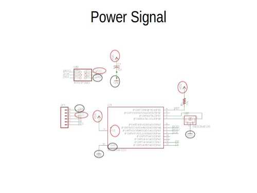
In a schematic you must designate how the electrons are flowing by adding VCC and GND points.
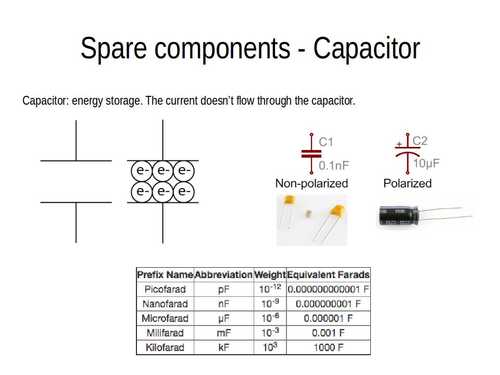
A capacitor is a little battery in your circuit. You can store some electrons there. When you release these electrons you amplify your signal. Capacitors can have both polarity and non-polarity. This is designated in the schemtic by their respective symbols.
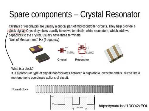
Resonator chrystal. A clock. The microchip is doing thousands of bit flips per second. This must be done in perfect timing or it will become a mess. Some ICs have resonators build in, other don’t, yet other’s again have resonators that aren’t accurate enough. In the last two cases you need to add a resonator to your circuit. It’ll orchastrate your ICs operations like a metronome.
The measuring unit is MHz.
The resonator does not have orientation. It is good practice to place it as close to the IC as possible because distance traveled over the trace equals a time delay. And time is exactly what the resonator is about. You must also try to place the two legs of the capacitor at equal distance from the IC. Equal distance is equal travel time and improves accuracy.
Remember overclocking from the early PC days? It means you are pushing the amount of cycles of your processor up. This would make your computer faster, but since you pushed it to it’s limits, you also had a bigger chance of it making mistakes.
Reading a schematic.
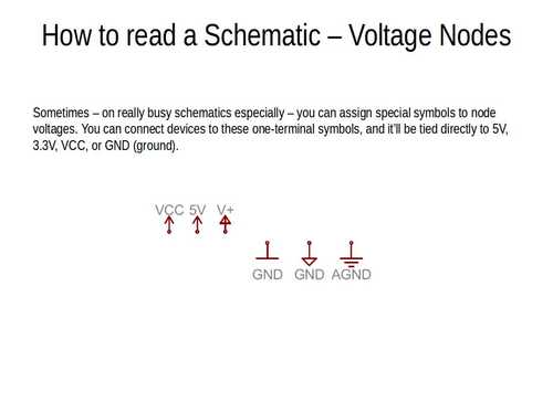
Power in a schematic.
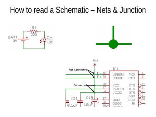
Junctions are indicated by a green dot.
You can indicate traces in your schematic either by drawing a line or by giving the ends of two the same name. Note that capitalization matters. Names have to be exactly the same.
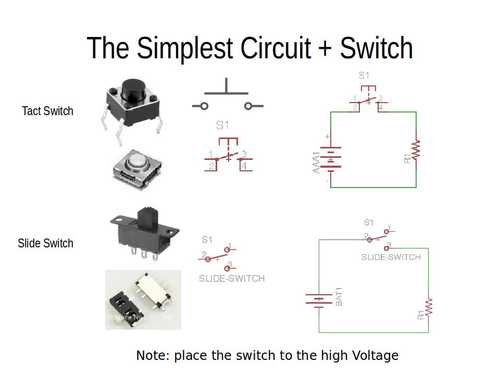
Switches are used to open and close the circuit manually. I used the tact switch in my circuit. It has for traces going out to it but I closed the upper two traces by ending the trace with the blue X in Kicad.
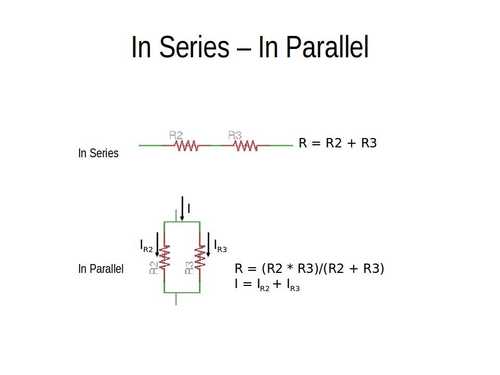
It makes a differences whether you make your schematic in series or in parallel. Mind that it is a different formula to caculate the value of the resistor.
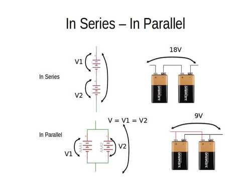
The same goes for power.
symbols
| fenomenon | symbol |
|---|---|
| Ohm | R |
| Volt | V |
| Amp | I |
| Watt | W |
| Resistor | R |
| Capacitor | C |
| Inductors | L |
| Switches | S |
| Diodes | D |
| Transistors | Q |
| Integrated Circuit | U |
| Crystals and oscilators | Y |
Laws
Ohm’s law I = V/R
Power: P = VI. Power is measured in Watt.
Group assignment
A full description of the group assignment can be found on our communual page.
For our group assignment we tested a multimeter, a powerbench and an oscilloscope. Next to that Henk demonstrated a logical analyzer to us.
For the testing device we used a board with an ATTiny44 chip containing a LED and a button. git
Test set up:
Goal: test the electronic current of the Tiny with the LED light blinking and when pushing the button on and off. The test set up consists of attaching the the power bench to the Tiny board and in addition attach the oscilliscope. And then read out the current flow on the oscilloscope.
Step 1: The multimeter
To connect the board to the power bench we first had to find the VCC and GND on the board. We used a multimeter to verify that. First we looked up the image of the board and looked where the GND was. We also looked up the datasheet for the Tiny44 to find the GND leg on the Tiny44. It is leg number 14.
We then double checked with the multimeter to see if we had indeed found the GND. We measured with the multimeter in continuity mode. We put the multimeter at setting 2 Volt. We then put one pen on the GND and the other pen on one of the FTDI pins. One beeped, so that must be the ground. Our educated assumption that it was pin 14 was correct.
Step 2: the power bench.
This device has its own power source and can be used to feed power to the device you are measuring. You can adjust the values by a turnable knob. We looked up the voltage needs for the Tiny board and saw it is 5V. We set the power bench to 5V and tried to clamp the aligator clamps to the device. This was hard. The clamps are made for larger electronic components then the tiny board we were testing. The overly large clamps remained a struggle throughout the test. We clipped the clamps to the VCC and GND on the FTDI header that we had located in the previous step.
After we connected the power bench at 5V to the board we had a read out stating that the board was drawing 5mA. This information you can use to calculate how long a battery will last when it is powering your board.
Step 3: Oscilloscope
An oscilloscope is a device used for testing electronics. Its main function is to display varying voltages running through a circuit. From Wikipedia “Oscilloscopes display the change of an electrical signal over time, with voltage and time as the Y- and X-axes, respectively, on a calibrated scale. The waveform can then be analyzed for properties such as amplitude, frequency, rise time, time interval, distortion, and others.”
Next we wanted to measure the current that flows through the LED. The LED was programmed to blink really fast. Our challenge was to get a read out of the current flow on the oscilloscope. We needed to connect the oscilloscope to the GND and to the leg of the ATtiny44 that is connected to the leg. This leg was easy to find as we could just see with our eyes and follow the copper trace that connects the LED to the chip.
We then measured the voltage that ran through the LED with the multimeter. We held each probe pen on one side of the LED. We set the multimeter at setting 2V because the datasheet said the LED is 1.8V. We measured 0.8V. We figured that since the LED is blinking fast, the measured voltage was lower than the LEDs specifications as it oscillated between on and off. We located the VCC side of the LED by looking for the green stripe on the component that indicates the VCC. We used a magnifyer glass to see it.
We then used the oscilloscope’s alligator clamps to connect the GND of the osciliscope to the GND of the board. And then made contact between the probe pen of the osciliscope and the leg of teh ATtiny44 that connects to the LED.
We turned on the osciloscape. Then turned the voltage setting until we saw a flat line. Twice we made a short. This happened because the large pen of the oscillator was hard to keep in the right spot. The board stopped blinking and we thought we’d broken it. But it was the powerbench that had shut itself off. We surmised that the powerbench has a build-in safety feature that it stops powering when there is a short.
We first set the osciliscope on 100 mV. We saw the the jumps between the voltage going from flat to top. We then changed the setting to 2V with the turning the knob Volts/Div turning knob. And then altered the timing with the Time/Div button until we saw the squares.
The best representation of current flowing through the LED was at setting 2V and timing 2.5 milliseconds. We could now clearly see the representation of the blinking LED as we saw the line on the osciliscope go up and down.
One square on the grid of the display depicts the measured unit. In our case we had set it to 2 Volts. So 2.5 squares in the picture refers to 5 Volt. The time was set at 2.5 milliseconds. And the panel said 50mA.
Logical analyzer
Henk demonstrated a logical analyzer to us. This is a nifty device that can read out bits. In the final instance bits are nothing other than a transistor switching on and off. The logical analyzer measures this on and off switching and represents them in software. It groups the bits in bytes (8 bits). In our case the analyzer was tracking an echo operation on the board. When connected to a computer and you type in something, the board echo’s that message back.
In the software of the logical analyzer we could see the bits represented as on (current flows or 1) and off (current does not flow or 0) in the form of visual stripes high (on) of low (off). Eight bits were grouped together visually divided by a vertical blue stripe in the software. Above the bytes the software translated the bits in to more easily humanly readable representations. Since the chip was sending letters (echoing what Henk typed on his laptop) the bits formed ASCII code. Each byte represents a single character. The software showed the characters above the bytes in the visualizer.
What I learned from the group assignment
I learned new settings on the multimeter. I had used one in week 04 to debug my board. This week a learned how to use the continuity setting. You set the meter on a voltage that is closest to what the board or component is using. So to measure a 1.8V LED you set the multimeter to 2V.
I learned the function of the powerbank. It powers the device you want to test at the voltage you decide. You can use the power bank to calculate how long your battery will last with your electronic system.
The oscilloscope was interesting too. You can see how the voltage changes over time and can deduce information from it. You can fine tune voltage and time and see how the current runs through your board.
Most interesting was the logical analyzer. It is amazing to see a device reading out the operations in a chip by translating the the current flow into bits. I now understand better how people do reverse engineering of software. With a logical analyzer you can capture the machine code that is happening on a chip. If you can translate that into higher level code, you can figure out how the software works. I also heard that there are some forms of spying whereby measuring the electric field around a device captures what inputs a human gives to the device. This happens for instance in the fiction book Cryptonomicon by Neil Stephenson. But it also happens in the real world. I’ve read news articles about academics doing it for researcher purposes (can it be done and can you defend against it). And if I am not mistaken I also think one of the disclosures of Edward Snowden about the NSA was that this was one of the weapons in their arsenal to spy on electronic communications. Better understanding how technology works is one of the reasons why I came to FabAcademy. I like that I now better understand how electrical eaves droppping works. Those kinds of news articles interested me because of the implications for society. But now I don’t just know that it can be done, but have a little bit better understanding of how it is done.
Individual assignment: redrawing an echo board
Description of the individual assignment: Redraw one of the echo hello-world boards or something equivalent, add (at least) a button and LED (with current-limiting resistor) or equivalent input and output, check the design rules, make it, test it.
Learning Outcomes
Select and use software for circuit board design
Demonstrate workflows used in circuit board design
Have you?
- Documented what you have learned in electronics design
- Explained problems and how you fixed them, if you make a board and it doesn’t work; fix the board (with jumper wires etc) until it does work.
- Included original design files (Eagle, KiCad, - whatever)
- Included a ‘hero shot’ of your board
- Loaded a program and tested if your board works
Choosing an echo board
The first step is to choose which echo board to make. This week’s index page of the class links to a list of Echo boards we can make. There are several versions of the ATtiny chip and several ARM chip based boards. I am foregoing the ARM chips because they are harder to make. I really like we are now on the stage that we are designing our own electronics boards. But I have never done it before and I do not know how difficult it will be. Therefore I am choosing a simpler board. This also excludes the ATtiny1614. It is a newer ATtiny version and that means there is less documentation for it. That leaves the ATtiny45 and the ATtiny44. The 45 has an 8 pin chip, whereas the 44 has 14 pins. More pins means the chip can do more operations because it has more pins to communicate through. Therefore I choose to make the ATtiny 44 Echo board.
There are two tiny44 Echo boards on the above mentioned page. One is the 44.2. This one has a board with two layers of traces, on the top and the bottom of the board. As I said, I sticking with ‘beginners level’ for starters, so I choose the 44 board.
Preperation for redrawing the ATtiny44
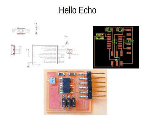
The first thing I do is get an idea of the board. Using the files provided for the board on the FabAcademy index page for this week (see above). Here is an image of the board representation is given and a picture of a finished board.
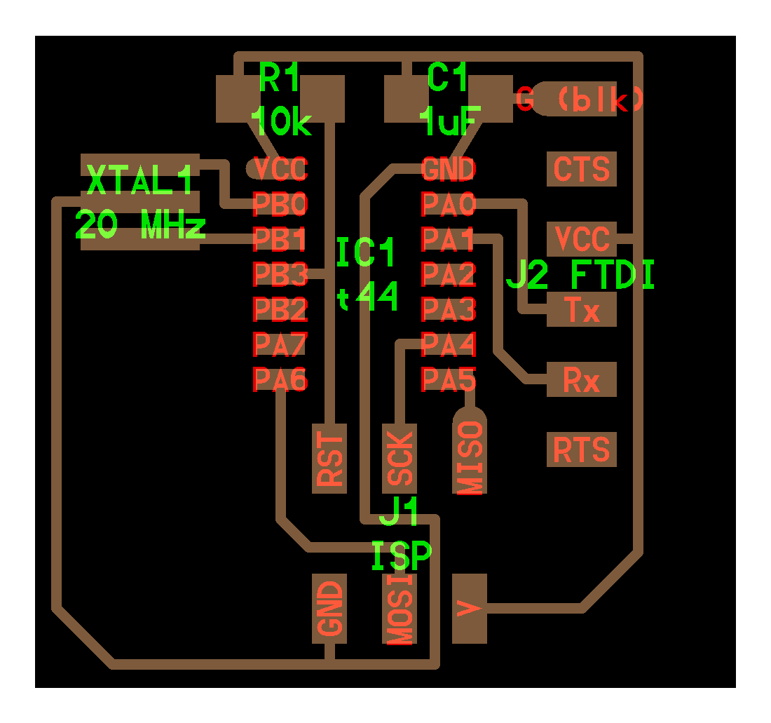 Representation of the board from the Fab page.
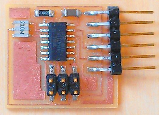
Picture of the board from the Fab page.
Components
I assemble the list of components of the echo board. There is a Fablab inventory list of all the components that available in every FabLab in the world. The components of the echo board are on that list.
First I look up the ATtiny44 IC. On the component seller Digikey site you can see there are many different types of ATtiny44’s. But there is only one ATtiny44 on the Fablab inventory list. So I assume we are using that one.
For the other components I look at the image of the board. There is an R1, R means resistor. It says 10k. So I need a 10k resistor. I look it up in the Fab inventory to get the specifications. These are: RES 10.0K OHM 1-4W 1% 1206 SMD. This means: RES > resistor. 10.0K OHM > a 10 thousand resistor measured in ohm. 1-4W > the resistor can handle between 1 and 4 watts. 1% > the wattage can deviate by 1%. 1206 > this specifies the form factor of the component, namely the size of it. SMD > again about the form factor this time the type of packaging: it is surface mount soldering (contrary to through-hole).
The next component is a capacitor (C1 on the board). It states 1uF or 1 microfarad. There is only one of those on the inventory list so I’ll use that one.
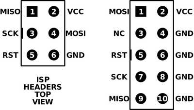
I don’t know how to read J2 FTDi and J1 ISP from the board. J is not a letter that refers to a component. Using CTRL F (find) on the inventory list does not offer either FTDI or ISP. I look at the picture of the board and see that the FTDI is a 6 pin connector. But that does not help me find it in the inventory list. I look on Rutger’s documentation. He refers to it as a 6-pin ISP header and a FTDI header. Searching for the keywords ‘header’, ‘6-pin’, ‘6 pin’ do not result in a hit in the inventory list. There are headers 1 row male horizontal but none of them have 6 pins. I also look at Henk’s page again the components are only refered to as 6 pin header and FTDI header. But I have no idea how to find this components in the inventory list based on that information. And with yet another FabAcademy student’s page I get none the wiser. I’ll leave it for now because this is costing to much time and there must be an easy solution. Hopefully I figure this out during the rest of the process.
On the page of Svetlana Shishkovets I find: 1 x 6 THT Pinheader. (This later turns out not to be accurate. The 6 pin is the ISP header. or maybe THT is another word for it.) I can’t tell from the board’s depiction what the XTAL1 20MHz component is. I go to Henk’s page again and see he used a 20MHz resonator. So I’ll add that to my component’s list.
Besides the components of the Echo board we also have to add an LED an on/off button and a photoransistor.
Later I look back at the slide show Henk shared with us. Here I see on slight 20 that all components are represented in the schematic and twinned with the components on the board.
Finding the components.
I am still not sure what the ISP header is. I look online and find on Wikipedia: ‘In-system programming (ISP), also called in-circuit serial programming (ICSP), is the ability of some programmable logic devices, microcontrollers, and other embedded devices to be programmed while installed in a complete system, rather than requiring the chip to be programmed prior to installing it into the system. It allows firmware updates to be delivered to the on-chip memory of microcontrollers and related processors without requiring specialist programming circuitry on the circuit board, and simplifies design work.’
This I understand, we are programming the IC while it is already part of the board. But what is the ISP header? The image on the wikipedia page shows the same schematic as our ISP header. (I did not finish the search for the meaning of the ISP header at this point.)
Source: By osiixy - Own work, CC BY 3.0
Note: Henk said in the local lecture that a LED needs a resistor. It is non-ohmic by itself. To calculate the resistor value for the LED you look in datasheet to see how much current it can handle and calcultate the resistor. Next I look up the orientation of the components. The IC has orientation. Resistors do not have orientation according to Henk. Capacitors vary accordig to the internet. (Later I found out that polarized capacitors have a different symbol than non-polarized ones.) Resonators do not have orientation according to Arduino forum.
| Components | Specifications | Orientation | Name |
|---|---|---|---|
| ATtiny44 | ATTINY44A-SSU-ND | Yes | IC1 |
| Resistor 10k ohm | library: RESUS-1206. Inventory list: RES 10.0K OHM 1-4W 1% 1206 SMD | No | R1 |
| Capacitor 1uF | CAP CERAMIC .1UF 250V X7R 1206- | C1 | |
| Resonator 20MHz | CER RESONATOR 20.00MHZ SMD | No |
XTAL1 |
| ISP header 2x3 | AVRISPSMD | ISP | |
| FTDI header | FTDi SMD header | yes | Can’t name |
| LED | Yes, indicated by a green stripe | LEDred | |
| Resistor 5k for the LED | ? | No | R3 |
| Switch | S1 | ||
| phototransistor | SENSOR1 | ||
| Resistor 10k for the photosensor | RESUS-1206 | no | R2 |
Differences between my component table and the example sketch:
- a different switch
- 3rd resistor
I don’t feel that I know all that I should know before starting to draw a circuit. But I’m firing up KiCad and see where I’ll run into a wall.
KiCad.
Henk gave us an introduction so the first steps have been explained.
Adding the Fablab library
There are component libraries in KiCad but you can also import your own specific libraries. FabLab’s have a library with all the components of the standard inventory of all Labs.
1. I download the library from https://gitlab.fabcloud.org/pub/libraries/electronics.
2. Then I go to Preferences > manage symbol libraries > project specific libraries and then clicking the downloaded .lib file.
Note that the library is added to this specific project. When you make a new project you have to import the library again.
Main menu KiCad’s main menu consists a number of icons. The icons are organized like the workflow of designing a board. You start with the schematic, then your PCB, etc.
 Main menu of Kicad. From left to right: schematic layout editor, symbol editor, PCB layout editor, Footprint editor and a view others that we won’t use this week..
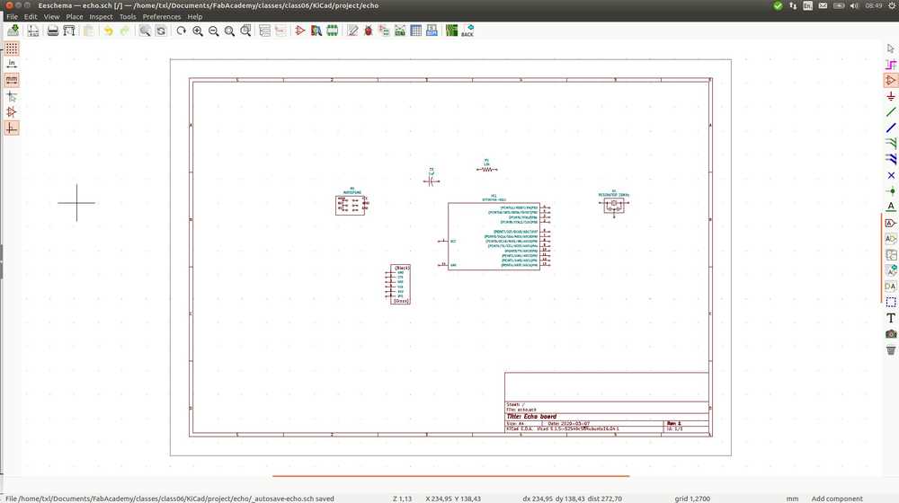
Schematic Layout Editor
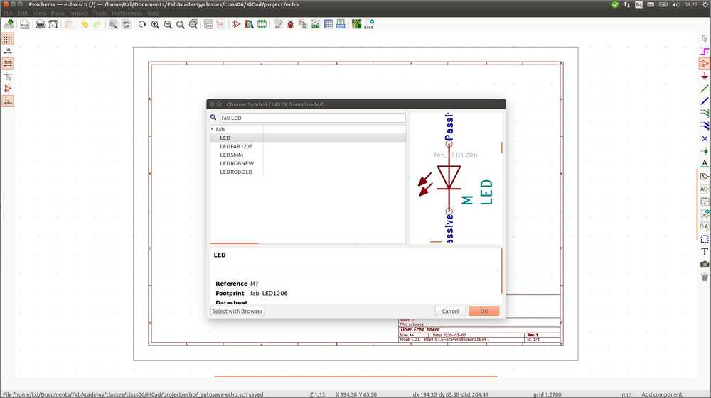
I found all 6 components in the library and placed them randomly on the schematic.
Next I have to add the extra components we must add to the Echo board for the assignment: a LED, a resistor for the LED, a button and a phototransistor. When opening the Fab library there are several LEDs. I think it should be the 1206 LED because that is the form factor we are working with. But I’ll check with other student’s documentation. Both Henk and Rutger have the 1206, I consider myself double checked.
I want to add the second resistor that goes with the LED and notice there are several types of resistors in the fab library. Back to other people’s documentation to see which one I need. Based on that I choose the RES-US1206. It is the form factor we use and Henk used it too. But I must say that I see no logic in it. There is also a RES-US1206FAB and a RES-US1206W. Why not use either of those?
Next up the button, or switch. Button does not yield any results in the library. SW for switch is the right querry. It results in a 6MM_switch, a SPDTSWITCH and a SLIDE-SWITCH. Going to the Google docs inventory list I see four switches. They don’t seem to align to the ones in the library: in the inventory we have a SWITCH SLIDE SPDT 12V, SWITCH SLide SPDT 6V and SWICTH TACT SMD W-GND 160GF. Again I have no idea which component to pick. Going to Henk’s page I see he used one that had 6mm in the name. Rutger too mentions 6mm. I’ll go for that one then but again fail to see the logic of how one would figure this out if you had not other people’s documentation to look at. After having placed the switch, the symbol looks very different from the ones on Henk and Rutger’s schematics. They used a slide switch. So I delete the 6MM switch and add the slide switch.
There is only one phototransistor in the library so that one is easy.
I then go on to name/annotate the components. (See step 3). In the example of the Echo board, the resonator is named XTAL1. This corresponds to a description of one of the pins of the IC. I copy this naming style but I also add the name resonator for my own remembrance. I suddenly realize that I might have mixed up the resonator and the capacitor in my head. The resonator is the clock that helps the IC do it’s operations on the right timing. The capacitor is a tiny power storage where electrons can be temporarily stored. Looking up the capacitor in the slide show of the local lecture I see I have not switched them up. I also see that there are two symbols for the capacitor: one symbol depicts a polarized (with orientation) capacitor, the other a non-polarized one. Looking at the symbol in the example schematic I now know that our capacitor does have orientation. I add that knowledge to my components table above.
I count the number of components in my table and the number of my components on the schematic. 10 for 10. Most components I named along the way but there are a few left to name. I add the names to the components table. I add a name to the FTDI header but it does not show on the schematic. I’ll leave it unnamed for now.
I read Anne Vlaanderen’s page to get an idea of the next step. I read ‘I received an existing schematic as a .png.’ I then realize Henk send this to us over Slack as well. Having remembered that a bit sooner might have made the process I just finished a bit easier. Haha. Well, at least I can use it to check if I done it right. Based on the example I change the name for the phototranssitor from M1 to SENSOR1 as that is more clear. I also note that the example schematic does not use the slide switch but the 6mm switch. I stick to the slide switch for now as I like the simplicity of its symbol. It also depicts a different capacitor, the one that is non-polarized. I’ll switch that one out in my schematic because that is one less mistake to make during soldering. There are again two to choose from: CAP-UNPOLARIZED and CAP-UNPOLARIZED-FAB. I choose the former on a hunch.
I see the schematic has even a third resistor. I don’t know what for. I’ll add it in my component table with ?? as a reminder. In the schematic it is attached to the sensor. Let’s keep that in mind.
I too rename my ISP ISP instead of M1. More clear.
 The example schematic provided by Henk.
My schematic now looks like this:
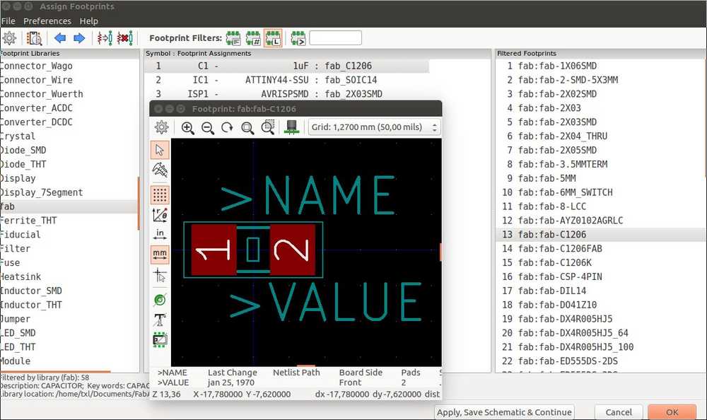
Assigning footprints
The next step is to assign footprints to the components. I remember Henk explaining us that you have to tell the schematic what type of formfactor you use. For instance SMD or through hole. But I am not exactly sure how to do this and where to pay attention to. I know we only use SMD not through hole. On Henk’s documentation page he speaks of adding the .mod file. I’ve seen the .mod file in the fab library directory I downloaded.
Adding footprint library
One of the icons at the top of the page depicts the footprint editor. Click it. Preferences > manage footprint libraries to add the .mod file.
Go to project specific libraries and click the directory icon and select the fab.mod file.
Choosing for instance LED gives us a bunch of options. Again not sure what to choose. There is the fab-LED1206 and the fab-LED1206FAB, which has smaller pads to allow for traces underneath, it says). Point is that when I click the LED and select properties in the schematic it says it already has a footprint: ‘fab_LED1206FAB;. So do I change it? Confirm it? Leave it? I don’t know.
No resonator shows up in the footprint editor. Right-clicking the resonator in the schematic tells me a footprint is already assigned.
The same goes for the ATtiny that does not show up in the library but has ‘fab_SOIC14’ already assigned to it in its footprint field.
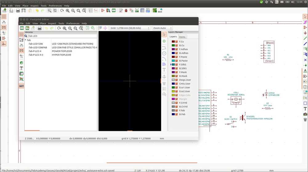 Footprint editor.
Annotating schematic symbols
I go to Anne’s page. She has first done another step: Annotate schematic symbols. I look at the KiCad explainer page] to find out how to annotate the symbols. In the schematic layout editor click on the ‘Annotate’ icon at the top of the page (depicting a paper with a pen on it).
A window pops up and the explainer page says the default settings are fine.
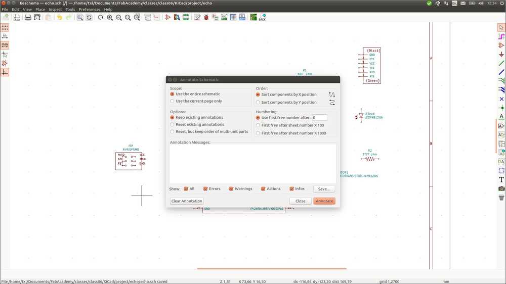
Annotate schematic symbols editor.
Output of the annotation editor.
Wiring
I then proceed to do the wiring (and leave the footprinting for now). Henk explained this. You either draw a line between two components or give them the same name to indicate they should be connected. Beware that naming must be exactly the same and capitlization matters.
Wiring is done by selecting a pin and pressing W, press K to end wiring.
Right-click cancel to remove a wire.
I heavily rely on the example schematic to do the wiring.
 My first wiring.
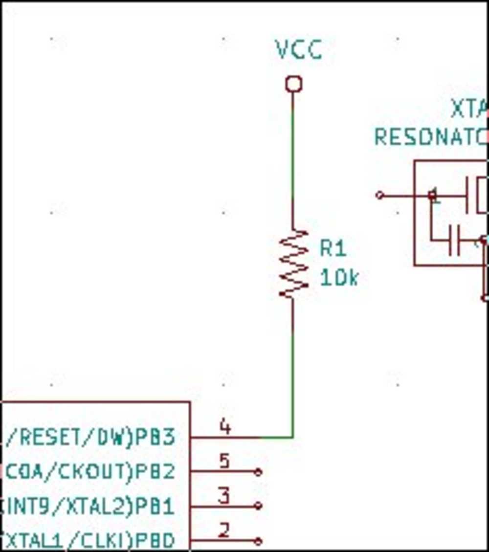
Next up wiring the resonator. The IC has two pins that say XTAL1 and XTAL2 respectively. The resonator also has an XTAL1 label.
Next I am labeling the pins of the IC. Draw a wire, end it and then richt-click to add a label. You can choose between label and global label. I looked it up and global label means the label counts across all sheets. Since I am doing a single sheet project, I’ll go for the normal label.
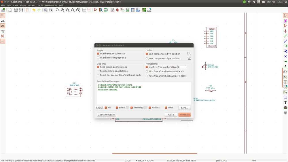
I get to the switch and I decide to replace the slide switch for the one used in the example schematic after all. I understand the schemtic better with the new 6mm switch. Pressing the botton will close the circuit. Whereas with the slide switch in Henk’s schematic, both pins are connected with a wire to each other. I don’t understand how the slide switch then can open the circuit (to put the device in off). So I replace the switch, annotate it, run the annotation editor for good measure and update the components table.
The annotation editor accepts my annotation for the switch, but annotates the newly added VCC. This tells me to run the annotate editor again after I am finished.
I add an extra resistor R3 to the sensor part of the circuit simply because the example says so. I would not have come up with that myself. I give it value 10K ohm because the example says so. I switch the names R2 and R3 because the the 2 10k resistors have consequetive numbering.
I run the Annotation editor and here is my schematic:
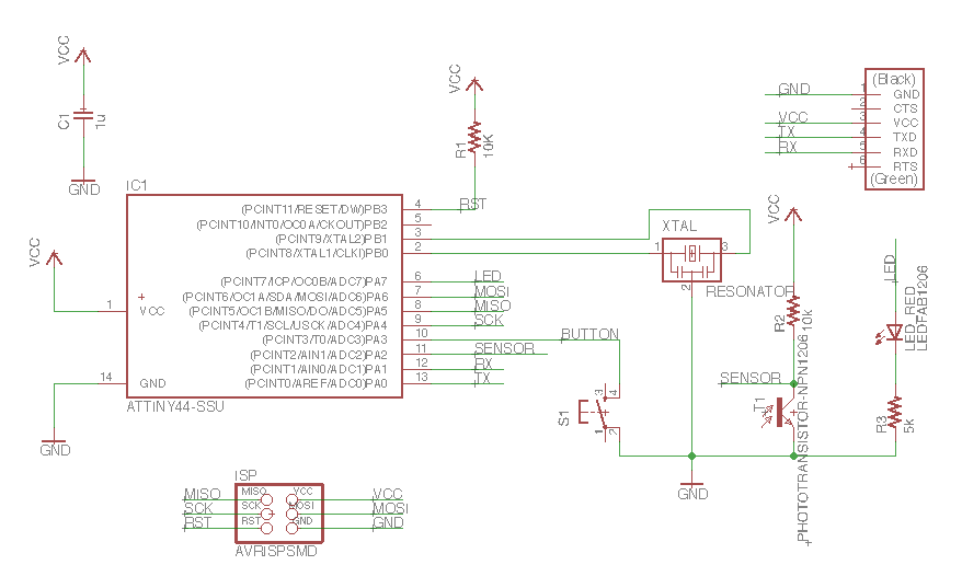
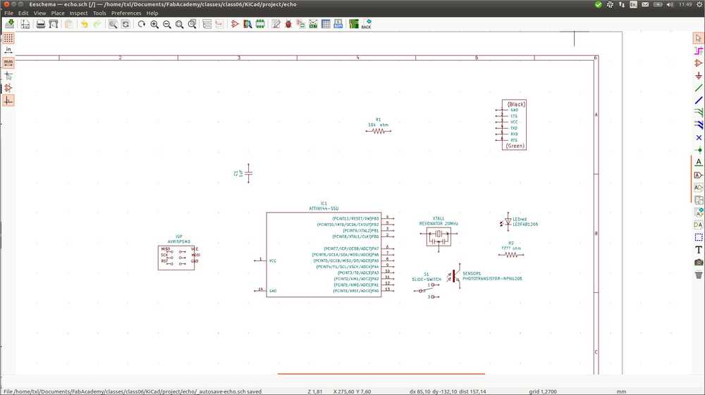
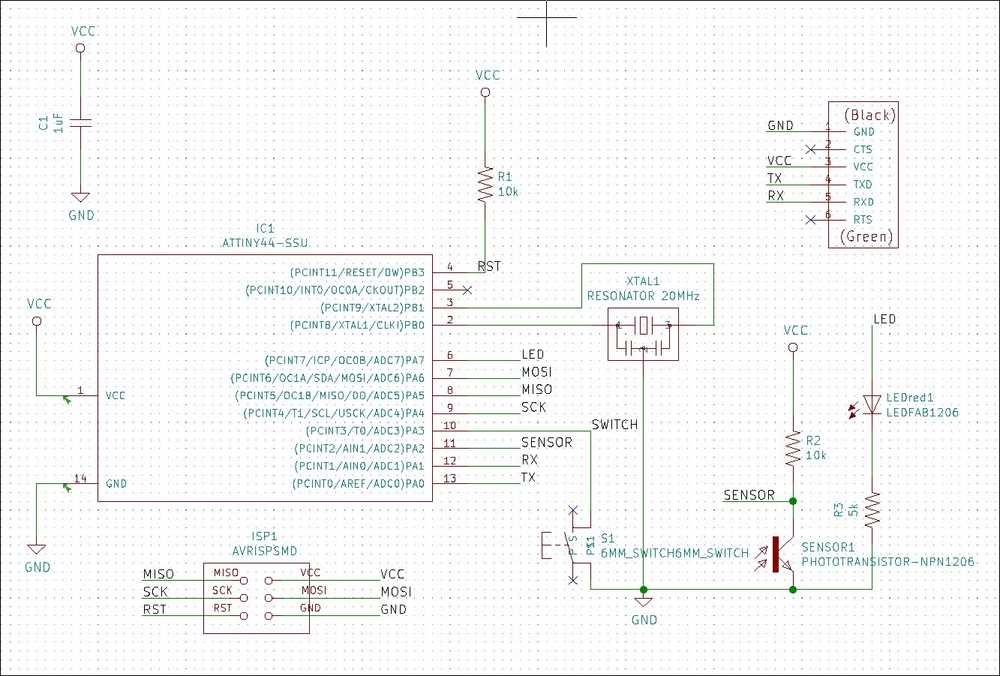
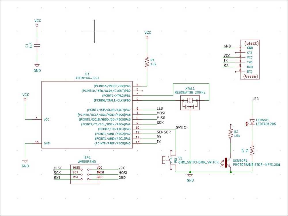 My finished schematic.
I added RST to one of the wires of the ISP but have not added that anywhere else. I realize it is the reset pin. Must I add ‘RST’ to the wire of the reset pin on the IC? Yes! I also forgot to add VCC to the R2 resistor.
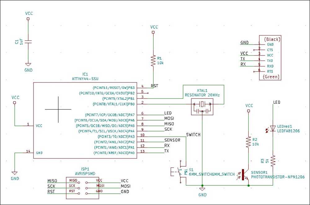 My finished schematic version 2.
Assigning footprints part 2
I go back to assigning footprints. I see that I made a mistake the first time around. I selected the footprint editor. But looking at Anne’s page I see I need the Assign footprint PCB footprints to schematic symbols icon.
 .
.
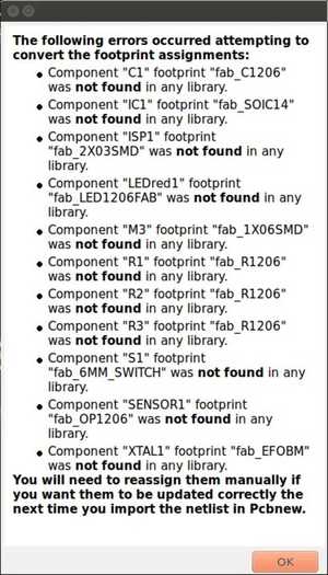
When I click it, there is a message saying:
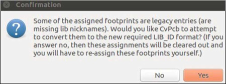
There is a long list of errors:
I deactivated the footprint library of fablab (fab.mod file) that I had added to the footprint editor earlier. I figured that maybe this was an older way of doing it (I got it from Henk’s pages in 2018) and now the footprints were maintained in another way. I deactivated the library under footprint editor > preferences > manage libraries. Now when I run the Assign footprint to PCB I get the same warning message, but the error message does not appear.
 Assign footprints with .mod library active.
There does not appear to be a difference. I’ll go with the one that does not give an error message and leave the library INactive. Hmm then I try to reproduce this but now both options give the error message. I’ll proceed with library ACTIVE and see where it will lead us.
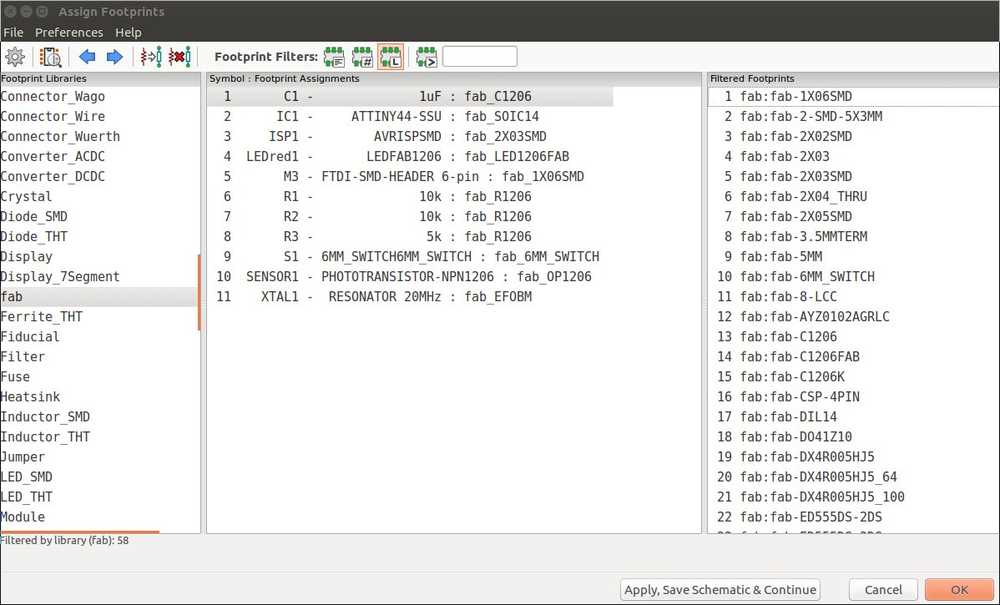
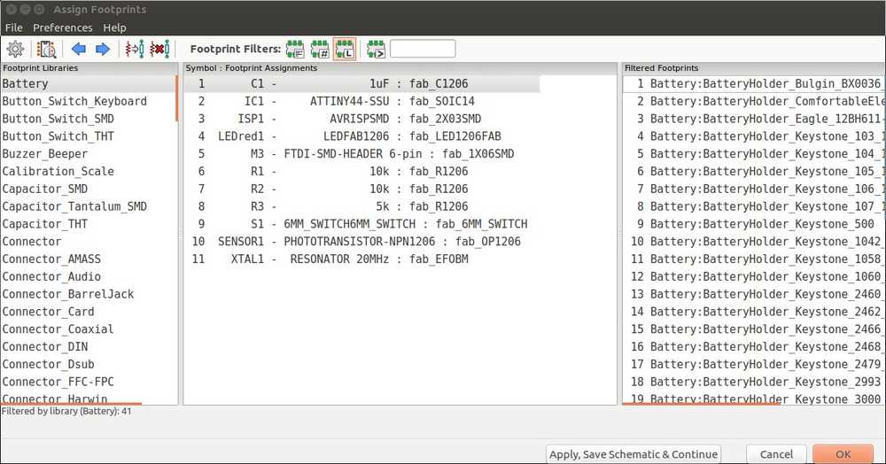
Assign footprint window: to the left the fab library is selected, in the middle the components, to the right the footprints from the fab library.
The difference I see is that the footprints of the components have underscores whereas the ones in the library have dashes. Should a reassign new ones?
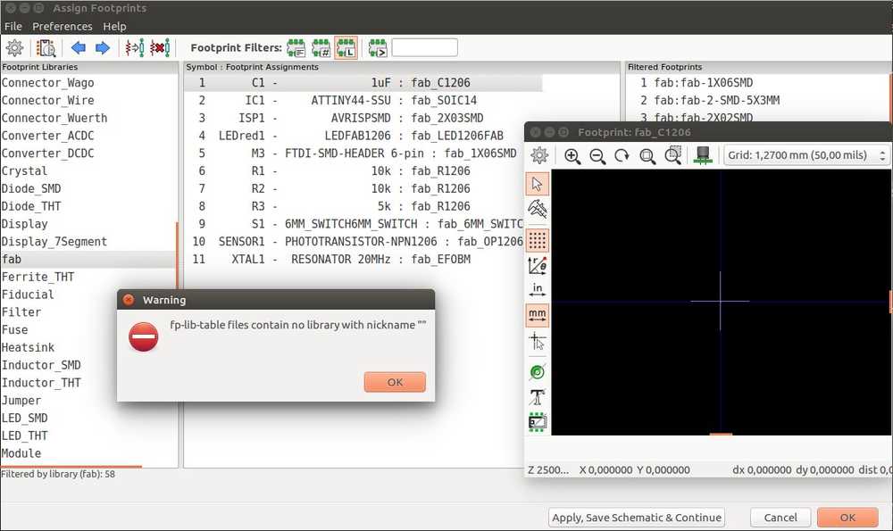
I inspect the footprint of the capacitor in the middle by clicking the icon with the magnifying glass on the upper left. This gives an error message.
Doing the same for the footprint in the library does yield a result. I decide to assign the footprints from the library to all the components. Now the only question is how. Well that is easy: select the component in the middle, select its footprint in the right pane and double click.
I assign footprints to all the components. I search for a footprint that is almost the same but has the dash instead of an underscore. After I have done that I click Apply and continue and then ok. I close the editor and then re-open again. There is no error message this time. Hopefully this worked.
Electrical rules check.
You can have KiCad do an electrical rules (ERC) check by clicking the icon with the lady bug (lieveheersbeestje) on it and click Run. This will check if your design makes sense. I have 8 errors.
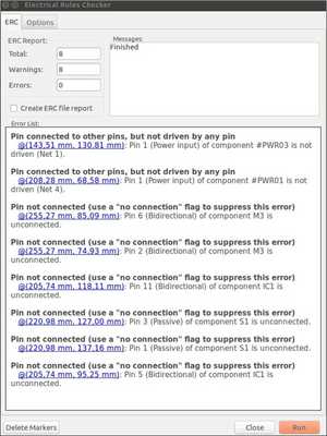
Pin 1 & 3 of the switch are not connected. I apply the no-connection flag. This is a ‘special component’ represented by the blue X on the right-side icon menu bar. I run the ERC again and these two errors disappear.
Same procedure for pin 5 of the IC.
It speaks of the M3 component but I did not name any component as such. I CTRL-F it in the Netlist and see that the FTDI header is referenced as M3. And indeed, there are 2 open pins. These are also indicated by the ERC by little green arrows. Two more errors gone, three to go.
The next error is pin 11 on the IC that should connect to the sensor. Looking at Henk’s page and then the eaxmple schematic I see I missed to draw a line for the senor. The IC pin is connecting to nothing at the moment. So I add another line and label it SENSOR. This solves the error.
This leaves me with to error messages about power inputs. The GND of the capacitor is not connected and the VCC of the IC. On Rutger’s page I read that this may be caused by there being no power net assigned to the GND and VCC. He found out about power flags. These are a symbol in the component library with a special function to tell KiCad that pins that require power are indeed connected to power. Source.
The powerflag does not improve things but makes them worse. I now have a severity warning.
Rutger also mentioned on his page that his instructor (Henk) told him that the power errors are not a problem. They are there because there is no power input. So I’ll remove the powerflags which made it worse and leave it at that.
I click annotate again.
(The next day I asked Henk about the power errors. Usually you would add a battery as a power source. But on this board the FTDI is giving power. KiCad does not know that but we do therefore we can ignore the power errors from the ERC. )
Generate netlist
The next step (Anne’s documentation is still my guide) is to generate a Netlist. In this list all information about the schematic is contained: components, their values, footprints, connections et cetera.
The netlist pop-up gives several options Pcbnew Cadstar and two more. I check Anne’s and Rutger’s page but neither specify which format they used. I am going with Pcbnew assuming that is the default. This results in a .net file that is placed in the project directory. You can open it in Gedit or another text editor and you recognize much of the statements like the library used, components, their values etc.
Final schematic
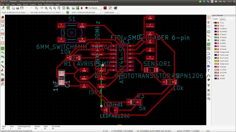
PCB Layout editor
We now go to the PCB Layout Editor and close the Schematic Layout Editor.
Open the Netlist in the editor bij clicking on the Netlist Icon (the one that says NET). Click Update PCB.
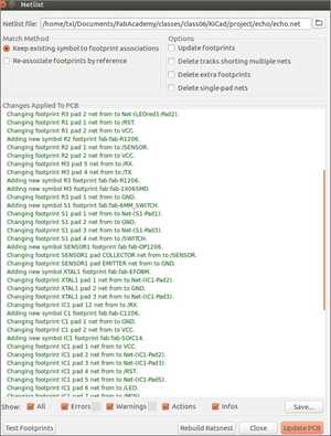
There is a whole list of changes.
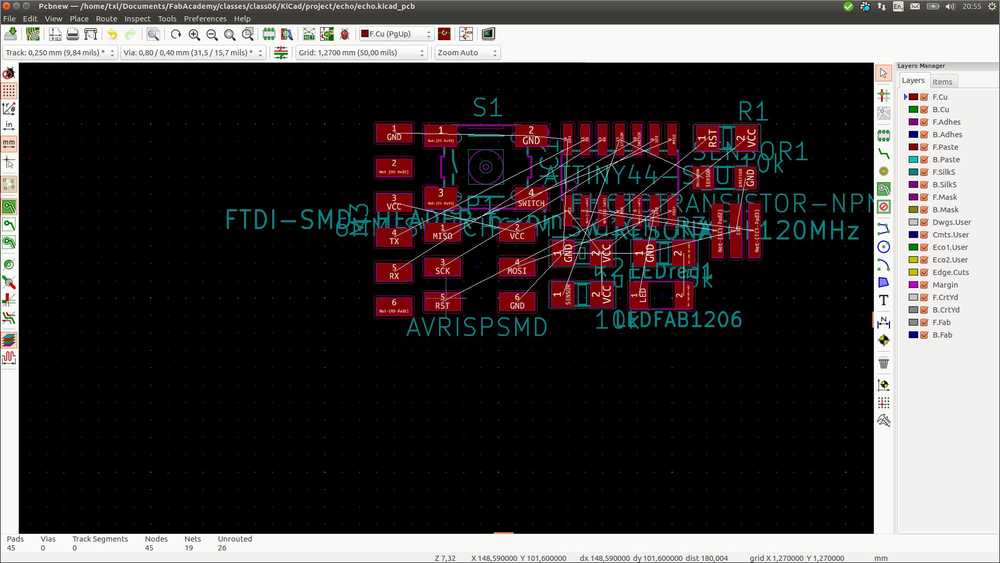 The components are placed on the field.
When you move the components to get a better overview, you can see the GND lines jump between components. That is because it does not matter which GND a component connects to.
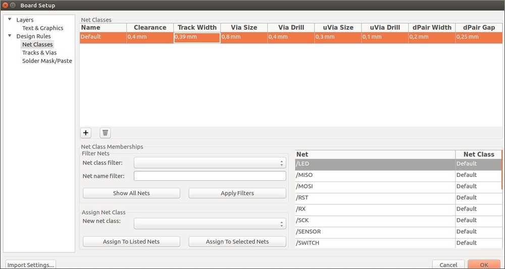
Set the design rules under the File > Board Setup. Here you enter the values of your milling machine. We have the Roland MX20. Henk told us during the local lecture: Under clearance you put 0.4, because the size of our drill bit is 0.4. You set the track width to 0.39. Slightly less than the drilling bit. We do not use the other settings on this job.
Henk told us to mind a few things when arranging the components on the board:
- Make sure traces do not overlap.
- You can run a trace under the resistor.
- Timing: even the smallest trace of copper takes time. Place the resonator and the resistor as close as possible to the chip and make sure the two traces are the same length.
- Make the board square for efficient cutting.
- Consider rotating the components to make the traces.
To place the components I use my schematic, the picture of the Echo board and the image of the board. I looked for a while at this puzzle and started to realize that people saying it’s a day long puzzle weren’t exaggerating. But is 10.00 PM on a Sunday an tomorrow at 09.00 AM I have to mill my board. On Henk’s page I read about an Autorouter! I research this. You need Freerouter which is used in Layout editor which requires Java installed. I go down this rabbit hole.
- Install Java on Ubuntu https://itsfoss.com/install-java-ubuntu/
- Download layout editor https://layouteditor.com/download
- On using Freerouter the source is https://techexplorations.com/blog/kicad/blog-kicad-5-how-to-use-the-freerouting-autorouter
Find Freerouter in the layout editor: Go to the directory where layout is installed: opt > layout on Ubuntu. In the layout directory go to the bin directory. Here you’ll find a file freerouting.jar. Click on that and Freerouter will start up.
Go to Kicad PCB new and export your project as an Specctra DSN file.
Double click the freerouter.jar file. Freerouter opens and asks to load a DSN file.
Click routing > autorouting
Oh! Wow! Fantastic!
Freerouter routes the board in steps over the course of seconds! You can see your schematic put into a board in front of yout eyes. In seconds! So long, day long puzzle! Best hack ever :).
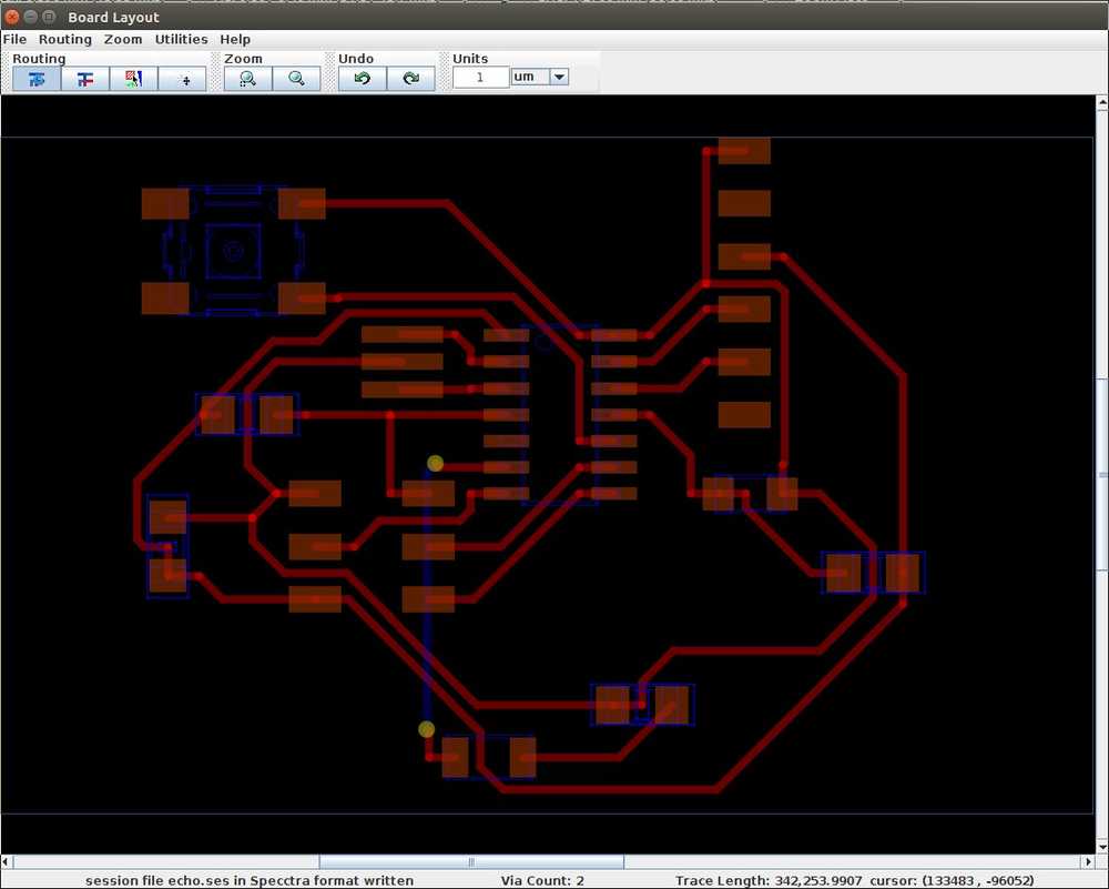 The board in Freerouter.
Export from Freerouter as a Specctra Session File.
The file is saved in the same directory as where you imported the .DSN file from. It is named filename.ses. It also creates a file filename.rules. This is the Freerouter file if you said yes to export rules.
Go back to Kicad pcbnew and file > import > spectra session.
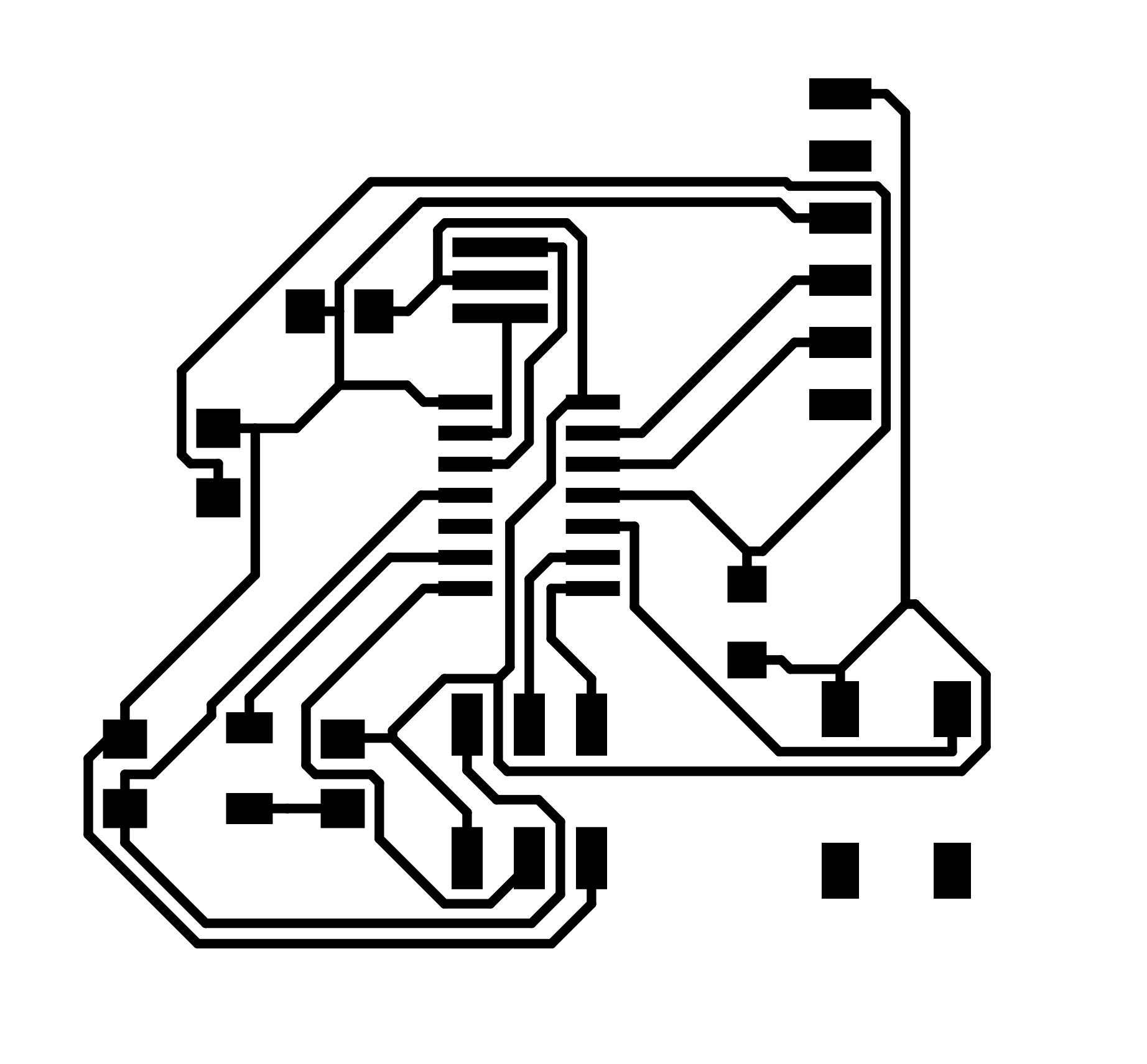
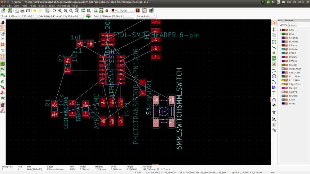
 The board in KiCad.
Kicad shows one green line. The line is a B.Cu line. F.Cu and B.Cu are both copper lines. Top copper is F.Cu Bottom copper is B.cu. Source. F.Mask is top solder mask, F.Silk is top silkscreen, etc. I am quite suspicious of that line. I don’t think it is correct.
I am going to have to get some sleep. Therefore I finish the process so I know all the steps. Then tomorrow I can do some trouble shooting.
I make the outline/cut out. That is actually a hassle. You have to click the add graphic lines icon on the left and select edge cuts either by double clicking it in the left pane or by selecting it in the drop down menu at the top. It won’t start drawing. There is something about hitting the space bar and then it will start. But it is unclear how it exactly works. I drew my cut out by trial and error.
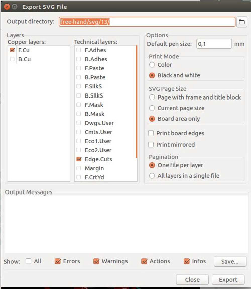
I then export to .SVG. You have to select export settings. An important one is selecting board area only otherwise you get the entire A4 schematic. Also black and white instead of color. For now I have to export both F.Cu and B.Cu files. But if you don’t have the green line in your schematic, you don’t.
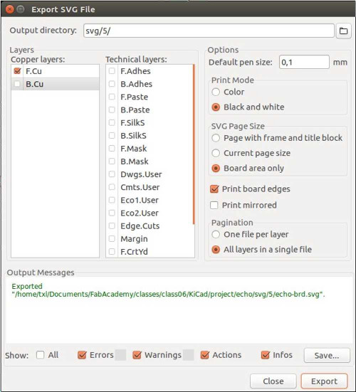
Export settings Kicad to SVG.
Debugging the board
Now I want to debug my board. As with FreeCad, KiCad does not seem to have an easy way to duplicate your project (the ‘save as’ function). I miss this because it means I either have to make a whole new project or start messing in the existing project that is almost good but not quite. On the KiCad forum I found that you can save your schematic (save sheet as) and your Pcbnew. But that is not the entire project as it is missing libraries. And perhaps other things too but I would not know exactly. By now my project directory has 14 files in it.
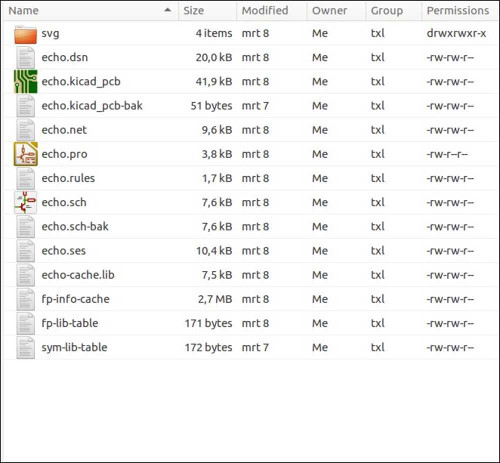
echo.dsn = exported DSN file; .kicad.pcb is the newpcb file; kicad_pcb.bak = ?; echo.net = netlist; echo.pro = project file; echo.rules = freerouter rules file; echo.sch = schematic; echo.sch-bak = ?; echo.ses = freerouter export; echo-cach.lib = libraries?; fp-infocache=?; fp-lib-table=?; sym-lib-table = ?.
Copying the entire directory seems to work. You can’t rename any of your files. I am a bit suspicious because usually in Linux the path is part of the file name. But at least I can fool around in copied versions of the project and if I find a solution apply it to the main project.
Debugging table
| Description | status |
|---|---|
| Export ratsnest before adjusting it & run through Freerouter | Done. Same result as first time. |
| Check schematic, is something wrong with the LED? | |
| Check if power errors are an issue | No. asked Henk. |
| Google Freerouter in FabAcademy site | That did offer results. Search these pages more often. |
| Henk forgot the design rules, maybe I forgot a rule too? | No. |
| IS the B.Cu trace not a problem. Is it okay it interconnects? Is Green just because it runs under a component ? | No. It turned out to be a via. |
| Put the LED locked in the place where Henk’s LED is and run it in Freerouter | That partly solved the problem |
| Fix manually | No need |
The solution was to fiddle with the Freerouter settings.
I checked Freerouter on the FabAcademy site. On a KiCad/Freerouter manual there I finally found an answer: the green lines and dots means Freerouter made a via. You can see it at the bottom of the Freerouter window: Via count: 2. So now I also understand that B.Cu probably litteraly means bottom trace, as in on the other side of the board.
Now that I know what is going on, I can search more targeted for a solution. I look online for how to disallow via’s. Either in KiCad or in Freerouter. On Freerouter.org I find: ‘Autoroute Parameter: Here you can define the layers which may be used by the autorouter, the preferred direction for traces on each layer, and if vias may be inserted by the autorouter.’
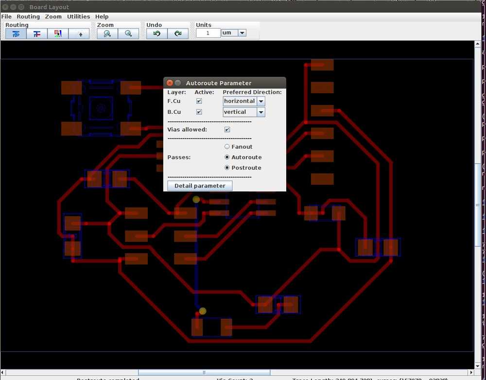
In Freerouter click utilities > parameter > autoroute and de-select via's allowed.
This time it takes a lot longer to route. I am at over a 1000 passes now. At after more than 7000 passes I stop the process. The manual linked to above also mentioned that you might want to try to rotate components yourself before running it in Freerouter. I watched the autorouting process and it does seem it does not try that by itself. From the manual: ‘If the Pass count gets above 30, your board probably can not be autorouted with this router. Spread out your components rotate them better and try again. The goal in rotation and position of parts is to lower the number of crossed airlines in the rats nest.’
I go back to KiCad and organize the components. I take cues from Henk’s successfull Freerouter experiment.
I export from KiCad and run it in Freerouter again. Still no dice, after many passes it has not found a solution. But I do notice something: it won’t try to make traces along side the cutout. That is to say, it seems to avoid making traces along the edges of the board. Perhaps the outline of the board is to close to components. Maybe design rules or other constraints prevent it from making traces there. I go back to KiCad to remove the outline trace. But in KiCad I see that the design was exported without the cutout ouline. So I go back to Freerouter, still on an outline hunch. I look under Utilities > parameter > select. Here I select board outline. I am not sure what it does but when I click autorouting, Freerouter finishes in seconds: postroute complete. I am a bit suspicious though… I mean, I selected board outline while my logic was that I needed to deselect outline. Selecting board outline is an extra constraint, I would think. Why would an extra constraint solve the puzzle?
I look in the Freerouter manual to look up what the selection layers that I just adjusted actually mean. Selection layers: ‘All visible: Items are selected on all layers with visibility factor > 0 (see also Layer Visibility). Objects on the current layer are preferred. Current only: Items can be selected only on the current layer.
At this point I packed my computer up to go to the FabLab. I did not further look into why this particular setting solved the puzzle. But it is clear that trying out different settings in Freerouter is useful.
In the FabLab I continued on. By now there had been so many steps in the process I was not sure about - from selecting the components, making the schematic, possible mistakes in pcbnew, the Freerouter solution - that I had no idea if the design would work. I decided to just continue and see where the ship would strand because I had no idea what to check for. Henk looked at my design and did not point out any mistakes, which was a bit reassuring. He then reminded me that we have to think about the orientation of the FTDI header. You must think about the fact that the programmer must be connected to it. And make sure they are both aligned in the same way. I had not thought about that. Checking the board of the FTDI on the online picture and matching it to my design, the orientation turned out to be right.
Harm reminded me that you must think about orientation of the components. I had another scare thinking I should have minded that during the design process. But then I thought that this is something that starts to count when the soldering step comes along.
Gimp
The next step was to export the project as .SVG from KiCad.
About these settings: Consider which layers you want to export. I only used F.Cu for the traces so I only need to select that. The other layer is Edge.cuts. You can choose the export each layer separately. Or you can export in one session by selecting one file per layer. This makes separate files for edge cuts and F.Cu.
Choose black and white instead of color. This is better for mods.
Select Board area only to only export the board and not the entire workspace.
Deselect print board edges. When selected the traces file will have an outline around them. Maybe the milling machine would mill those if you leave them.
I left print mirrored unselected.
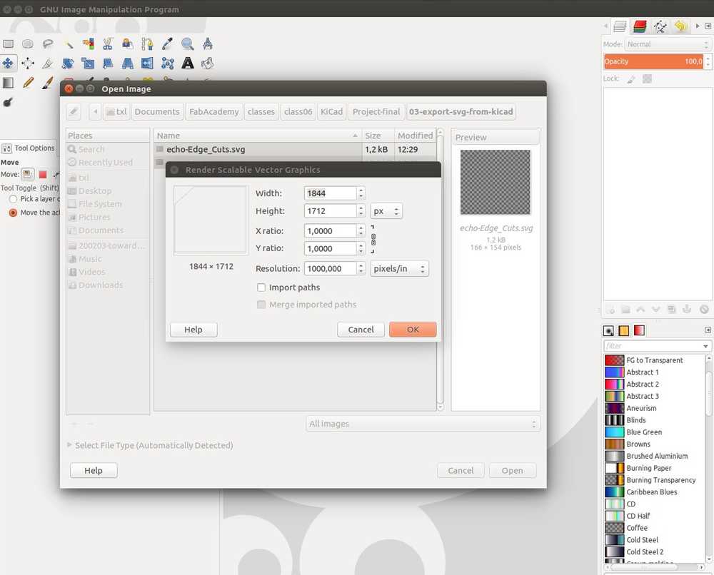
I then imported the .SVG into Gimp. It was very small only some 166 pixels wide. I spend a good half hour figuring out that you have to select set 1000 pixels per inch during import of the file. I found the solution on documentation pages of previous years.
I then removed the alpha channel. with layers > transparancy > alpha channel. I did not invert the image in Gimp but did that in mods.
You can also invert in Gimp by using colors > invert.
Make sure to export as .SVG or .PNG. You can not use .JPG because the quality is too low.
When this was done I transferred the files to the computer driving the milling machine. And used my documentation from week 04 to operate the milling machine.
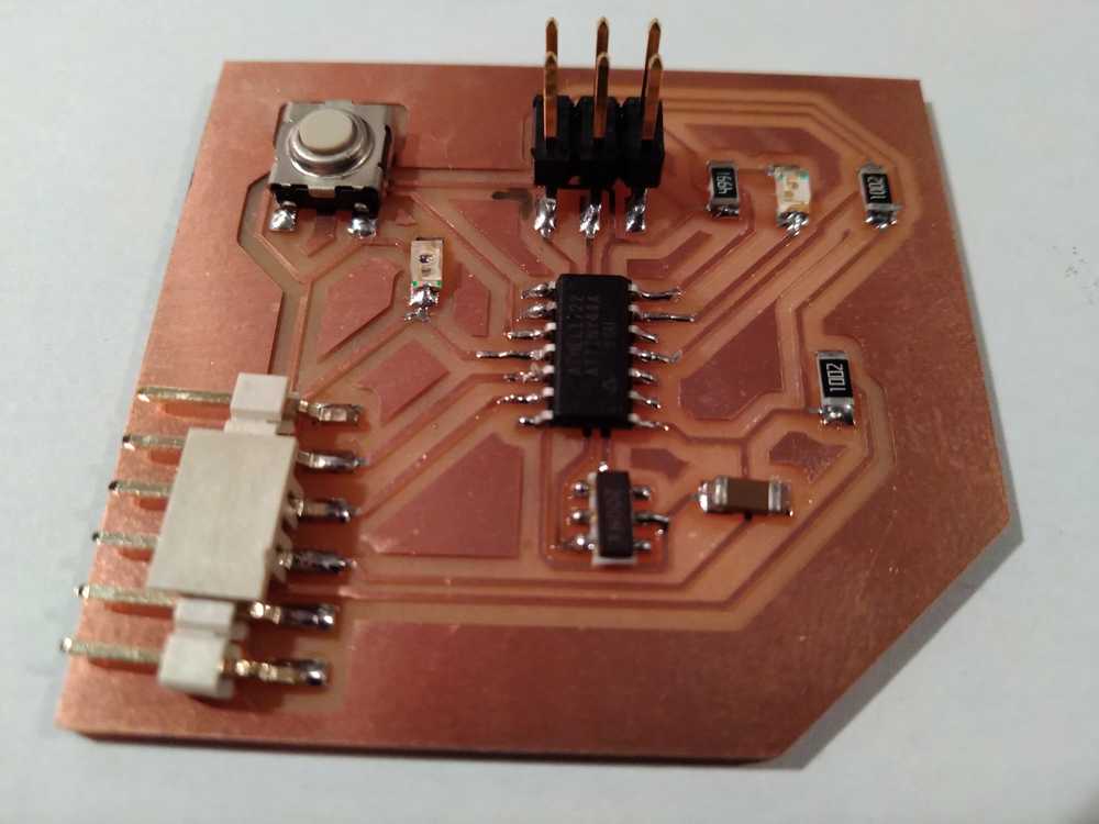
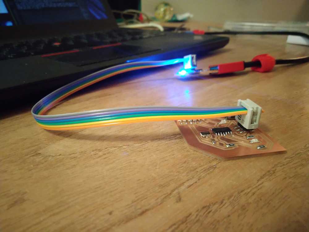
This is how the board came out.
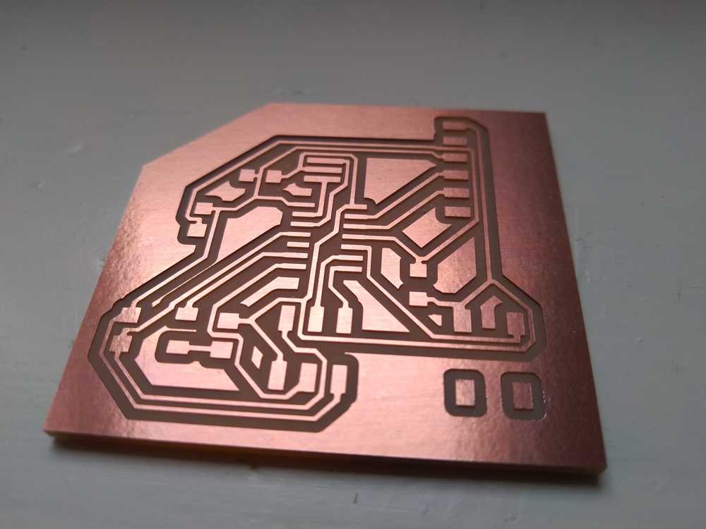 Echo board
Overview steps designing a board
This is a summary of all the steps described above for if I need them in the future.
Schematic layout editor
-
Edit page setting (second icon top left) I add date and name of the board.
-
Place symbols by selecting the
place symbolicon. .
Right click on the design field and the library will open. Add
.
Right click on the design field and the library will open. Add fabto your querry to look only in the fab library. Select a component and click somewhere on the design field to have the component placed there. You can move the components or rotate them via the right-click drop-down menu.
 .
. - Annotate symbols (or assign properties): select the arrow icon. Then select the component. You must draw a square around it to select, just clicking won’t work. Then right-click. In the dropdown menu choose
properties > edit properties. Here you can change name, value and other properties. It is good practice to name components with their standard names. R for resistor for instance. If you have multiple resisitor you name them R1, R2, etc. Under value you add the amount of ohms.
 .
. - Add values. Select a component and right-click
edit properties. Here you can add the value of your component. See the image of step 3. - Wiring: Select a component and press
W. Draw a line between to points you want to connect. PressKto end wire. Right-clickcancelto remove a wire.
The second way to wire is to give to ends of a wire the same name.
To add a VCC symbol you can either click the power icon on the left and select VCC in the library, or click the symbol selector and search for VCC. The VCC is displayed as a circel rather than the arrow in the example schematic. Henk’s page shows the same circel. I’ll leave it as such.
So the Reset switch is connected to VCC but there must be a resistor in between. - Annotate symbol editor: After you have done your own annotation you can ask the program to do automatic annotation, to complete all annotations. Click the
Annotate schematic symbols. icon at the top of the page (it’s a paper with a pen on it). A window pops up and the explainer page says the default settings are fine.
Annotate schematic symbols editor. - Add footprint library: Click the footprint editor icon (an IC symbol). In the footprint editor click
preference > manage footprint libraries. Add thefab.modfile (from my local computer), or another.modfile you downloaded. - Assign footprints: Click the
Assign footprint PCB footprints to schematic symbolsicon.. - On the left pane you see
footprint librariesselect a library, f.i.fab. - Select the component in the middle, select its footprint in the right pane and double click.
- Perform Electrical Rules Check: ladybug icon.
- Generate netlist. Click the icon on the top of the editor that states
NET.
PCB layout editor
- Import Netlist (icon).
- Set Design Rules.
File > Board Setup Design Rules>Net classes. For our Roland milling machine the settings are:Clearance 0,4 mmTrack width 0,39mm - Set cutout layer to 0.8 mm
- Update PCB from schematic
- Make sure grid is set to 1mm (or whatever value you prefer)
Manual routing:
1. Place components. Consider: connectors must be on edge of the board. Keep 7 mm board edge < > outer rim connector. Rotating components for easier tracing.
2. Click the wiring icon (green wire right side of panel).
3. Consider: running wires under components. Use 0Kohm resistors as bridges.
4. Perform Design Rules Check (ladybird icon).
5. Draw cutout. (Set Layers manager to Edge.Cuts; Use add graphic lines).
6. Set cutout line to 0.8 mm
7. Export to SVG. Mind the settings like board area only, black and white, de-select print board edges and select one file per layer.
Freerouter:
1. Export ratsnest as Specctra DSN file.
2. Import into Freerouter.
3. Route > autoroute.
4. Export from Freerouter as an Specctra Session File. It is saved in the same directory as from where you imported the DSN file as a .SES file.
5. Import .SES into KiCad Pcbnew file > import > Spectra session.
6. Perform Design Rules Check (ladybird icon).
7. Draw a cutout (Set Layers manager to Edge.Cuts; Use add graphic lines).
8. Set cutout line to 0.8 mm.
9. Export to SVG. Mind the settings like board area only, black and white, de-select print board edges and select one file per layer.
10. Make two seperate files: one for traces. One for cut-out by selecting one file per layer.
Gimp
- Open the SVG in Gimp. When opening SVG set 1000 pixels per inch to get a printable result. Source,
- Remove the Alpha channel in Gimp.
layers > transparancy > alpha channel. - Invert the the image to make white lines on a black background
Colors > Invertor invert the PNG in mods.
Soldering of the board
For soldering the board I start with figuring out orientation of the chip. There is a marking dot on the packaging of the chip. But to which pin does the dot refer? Looking in the datasheet of the chip did not offer up an answer. Henk then explained that the dot is also represented on the Kicad layout. Indeed it is represented as a purple circel.
The purple circel is the chip orientation mark in Kicad.
ISP connector orientation. I finally know what the ISP connector is. It is, well, a connector. Just a bunch of pins to connect a cable to the board. I considered orientation. I had written down ‘yes’ for orientation in my table. But now I think that it matters how you place the cable, but not how you solder the component. It being neutral pins that transmit whatever data the cable sends through them. I went and checked with Henk: it is just a bunch of iron captured in plastic, he answered. So, indeed, no orientation.
The phototransistor has orientation. I looked up the serial number which is 365-1157-1-ND. I found the serial number of the component on a piece of paper in the box where the transistors are kept.
Note: when buying components alsways keep the packaging with the serial numbers on it. Vital info!
Using that number you get to the digi-key site. They link to the datasheet. On the datasheet a mark is given that designates the collector side. In the Kicad board design I can see where the collector side is.
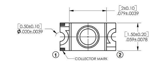
The collector side is marked with green stripes.
On the Kicad board, collector is also indicated.
Resonator: we have two boxes with 20MHz resonators. One box is labeled 20 MHz XTAL, the other 20MHZ resonator. We need the latter, it has a different footprint the the XTAL. The 20MHZ has three solder pads while the XTAL has only two. The serial number (s/n) is XC1109CT-ND. Looking on the digi-key site the component looks very different than the one in the picture. I also would expect it to say 20.0MHz but mine says 200Nx. I double check with Henk, but he says it’s okay to use this one.
Orientation: Datasheet. The resonator does not have orientation. I already looked that up and added it to my component table. But I do not trust my own table, so I hit the same answer online again: ‘Crystal and ceramic resonators are basically AC devices so there is no polarity issue in how you wire them up.’ No orientation.
Because the resonator has three pads at the bottom of the component I can’t solder it with a normal soldering station. I have to use the heat gun. Put solder on all three pads. Place the components on the solder and melt the solder with a heat gun.
Capacitor 1uF. No orientation. This can be seen from the symbol in the schematic. A capacitor with orientation has two different stripes. Our capacitor has equal stripes.
Resistor 10k. Resistors do not have orientation. The lettering says 1002, for 100 + 2 zeroes = 10.000.
The LED has orientation. Via the s/n number I find the product page and the datasheet.
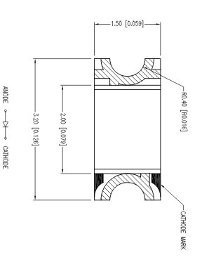
The cathode side is marked. In the schematic you can see the anode side is connected to the chip and the cathode side is connected to the resistor. The arrow in the datasheet depicts the direction o fthe current. The same arrow can be seen in the schematic.
Switch: the switch has orientation in that two legs are connected internally in the component. Make sure that that this aligns with the way it is depicted in the Kicad board. Datasheet
I figure out the orientation by checking the bottom view against my Kicad board. You can also look at the grey stripes at the bottom. The indicate the two connected legs. 
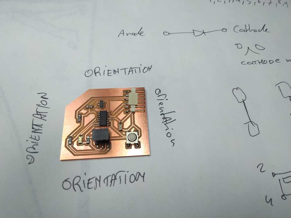
Final result after soldering.
Testing the board’s circuits
I used the multimeter to check if the traces worked the way as intended. You look at the Kicad board which trace should be connected. Put the probes of the multimeter on both ends. If it beeps, it works. You can also check between traces that oughn’t be connected. In that case it’s the absence of the beep that indicates the okay. I put the multimeter on the setting with an arrow and a musical note. The musical notes means it’ll beep. The arrow means current flow (I think). I was a bit worried that maybe I had put too much solder on the VCC pin of the FTDI pin header and that it would connect to the trace that runs from the phototransistor to the R2. I checked, there was no beep, so it went well. All connections seem ok.
Testing if the board works
 .
.
To test if the board works you have to connect it to the ISP we made in week 4. You must connect the two devices with a flat cable. This must be done in the right orientation which means connecting the two ISP pin 1s to each other. I worked out which was pin 1 of the ISP programmer in week04. It is marked with a dot on the schematic. That is, if you put the USB connector facing left it is the top left pin. I mark my ISP board with black pen on the side of the pin 1.
The pin 1 on the ISP is MISO, the pin 1 on the ISP header of the Echo board is also MISO. I go to Kicad schematic and PCBnew to see where the MISO/pin 1 is.
Pin 1 of the ISP on the Echo board is the one facing both the chip and the switch. I mark it with black marker on the board.
Connect the echo board to the computer and type.
avrdude -c usbtiny -p t44
I received output:
avrdude -c usbtiny -p t44
avrdude: Error: Could not find USBtiny device (0x1781/0xc9f)

avrdude done.  Thank you.
Some Henk help: I thought it did not see my echoboard, but it says it does not see the programmer. Turns out I had the programmer upside down in the USB cable. Now when I ran the avrdude command in the terminal I got:
Reading | ################################################## | 100% 0.00s

avrdude: Device signature = 0x1e9207 (probably t44)

avrdude: safemode: Fuses OK (E:FF, H:DF, L:62)

avrdude done.  Thank you.
Programming the board
To start talking to your board you have to:
- connect programmer to USB cable.
- connect pin 1 of the programmer to pin 1 of the Echoboard.
- run avrdude -c usbtiny -p t44 to start talking to the board.
I will use the Arduino program to try and program the board. I already have Arduino installed because of some Adafruit project I did in the past. On Instructables I find how to add ATtiny to the Arduino program:
Open: file > preferences
To add the board you add a library. The url for the library I found on Instructables. Pressok.
Next in Tools > Board > Board manager type in Attiny and install the library that shows up. Now the ATtiny should be in the list.
You also have to add the ISP programmer. Under Tools > Programmer. The USBATtinyISP was already in the library of my Arduino program.
Uploading the code: Under File > examples > basics I choose blink. This is a standard example code file in Arduino. It blinks a LED. This code is now visible in a new Arduino window. I press upload by pressing the arrow.
 .
.
This gives an error but I expected that. You have to name the right pin in the code, says the Instructables page. Following the example on instructables I change the code. You need to specify a pin number for the LED. I looked it up in Kicad and think it is pin 6.
/*
  Blink

  Turns an LED on for one second, then off for one second, repeatedly.

  Most Arduinos have an on-board LED you can control. On the UNO, MEGA and ZERO
  it is attached to digital pin 13, on MKR1000 on pin 6. LED_BUILTIN is set to
  the correct LED pin independent of which board is used.
  If you want to know what pin the on-board LED is connected to on your Arduino
  model, check the Technical Specs of your board at:
  https://www.arduino.cc/en/Main/Products

  modified 8 May 2014
  by Scott Fitzgerald
  modified 2 Sep 2016
  by Arturo Guadalupi
  modified 8 Sep 2016
  by Colby Newman

  This example code is in the public domain.

  http://www.arduino.cc/en/Tutorial/Blink
*/

int led = 6;

// the setup function runs once when you press reset or power the board
void setup() {
  // initialize digital pin 6 as an output.
  pinMode(led, OUTPUT);
}

// the loop function runs over and over again forever
void loop() {
  digitalWrite(led, HIGH);   // turn the LED on (HIGH is the voltage level)
  delay(1000);                       // wait for a second
  digitalWrite(led, LOW);    // turn the LED off by making the voltage LOW
  delay(1000);                       // wait for a second
}
This is the original file:
// the setup function runs once when you press reset or power the board
void setup() {
  // initialize digital pin LED_BUILTIN as an output.
  pinMode(LED_BUILTIN, OUTPUT);
}

// the loop function runs over and over again forever
void loop() {
  digitalWrite(LED_BUILTIN, HIGH);   // turn the LED on (HIGH is the voltage level)
  delay(1000);                       // wait for a second
  digitalWrite(LED_BUILTIN, LOW);    // turn the LED off by making the voltage LOW
  delay(1000);                       // wait for a second
}
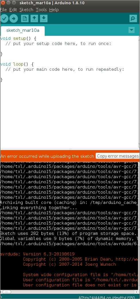
But it does not work. AVRdude warns:
An error occurred while uploading the sketch
Reading | ################################################## | 100% 0.00s

avrdude: Device signature = 0x1e9207 (probably t44)
avrdude: Expected signature for ATtiny24 is 1E 91 0B
         Double check chip, or use -F to override this check.
The mistake is that I have the ATtiny24 selected under the Tools instead of the 44. AVRdude gives that warning in its output. Henk also showed that AVRdude will warn you when your cable is inserted wrong. Run avrdude -c usbtiny -p t44 with your cable inserted wrong and avrdude will say:
avrdude: initialization failed, rc=-1
         Double check connections and try again, or use -F to override
         this check.


avrdude done.  Thank you.
I set Arduino to At44 and upload the file again. The file loads. Avrdude outputs:
avrdude: Version 6.3-20190619
         Copyright (c) 2000-2005 Brian Dean, http://www.bdmicro.com/
         Copyright (c) 2007-2014 Joerg Wunsch

         System wide configuration file is "/home/txl/.arduino15/packages/arduino/tools/avrdude/6.3.0-arduino17/etc/avrdude.conf"
         User configuration file is "/home/txl/.avrduderc"
         User configuration file does not exist or is not a regular file, skipping

         Using Port                    : usb
         Using Programmer              : usbtiny
avrdude: usbdev_open(): Found USBtinyISP, bus:device: 001:014
         AVR Part                      : ATtiny44
         Chip Erase delay              : 4500 us
         PAGEL                         : P00
         BS2                           : P00
         RESET disposition             : possible i/o
         RETRY pulse                   : SCK
         serial program mode           : yes
         parallel program mode         : yes
         Timeout                       : 200
         StabDelay                     : 100
         CmdexeDelay                   : 25
         SyncLoops                     : 32
         ByteDelay                     : 0
         PollIndex                     : 3
         PollValue                     : 0x53
         Memory Detail                 :

                                  Block Poll               Page                       Polled
           Memory Type Mode Delay Size  Indx Paged  Size   Size #Pages MinW  MaxW   ReadBack
           ----------- ---- ----- ----- ---- ------ ------ ---- ------ ----- ----- ---------
           eeprom        65     6     4    0 no        256    4      0  4000  4500 0xff 0xff
           flash         65     6    32    0 yes      4096   64     64  4500  4500 0xff 0xff
           signature      0     0     0    0 no          3    0      0     0     0 0x00 0x00
           lock           0     0     0    0 no          1    0      0  9000  9000 0x00 0x00
           lfuse          0     0     0    0 no          1    0      0  9000  9000 0x00 0x00
           hfuse          0     0     0    0 no          1    0      0  9000  9000 0x00 0x00
           efuse          0     0     0    0 no          1    0      0  9000  9000 0x00 0x00
           calibration    0     0     0    0 no          1    0      0     0     0 0x00 0x00

         Programmer Type : USBtiny
         Description     : USBtiny simple USB programmer, https://learn.adafruit.com/usbtinyisp
avrdude: programmer operation not supported

avrdude: Using SCK period of 10 usec
avrdude: AVR device initialized and ready to accept instructions

Reading | ################################################## | 100% 0.00s

avrdude: Device signature = 0x1e9207 (probably t44)
avrdude: NOTE: "flash" memory has been specified, an erase cycle will be performed
         To disable this feature, specify the -D option.
avrdude: erasing chip
avrdude: Using SCK period of 10 usec
avrdude: reading input file "/tmp/arduino_build_286757/Blink.ino.hex"
avrdude: writing flash (700 bytes):

Writing | ################################################## | 100% 1.07s

avrdude: 700 bytes of flash written
avrdude: verifying flash memory against /tmp/arduino_build_286757/Blink.ino.hex:
avrdude: load data flash data from input file /tmp/arduino_build_286757/Blink.ino.hex:
avrdude: input file /tmp/arduino_build_286757/Blink.ino.hex contains 700 bytes
avrdude: reading on-chip flash data:

Reading | ################################################## | 100% 1.41s

avrdude: verifying ...
avrdude: 700 bytes of flash verified

avrdude done.  Thank you.
I think the upload worked. But the LED does not blink. Maybe pin 6 is not right.
Instead of looking in KiCad-Pcbnew, I now look in the schematic. The LED has number 6 before it but also the designation PA7. Henk said something about the numbers of the pins not being the numbers of the pins. Now I understand that the numbers on the outside are the positions of the pins. But the PAx denotes the number of the pin.
I change the pin number in the INO file to 7 and upload again. And it blinks!
I also tried another program made by my class mate Harm. He wrote code to have the LED respond to the sensor. It loads but it does not seem to work. I check the pins but that seems correct. I leave it for now.
What I learned
Figuring out the components I got stuck. As I wrote in my documentation, rather than stubbornly insisting I figure it out before moving on, I decided to move on and see if I would figure it out along the way. In the first weeks I had a tendency to stand still when I faced an obstacle rather than move on. This time I moved on without having all the knowledge. It was a good decision as some knowledge gaps become clear along the way. It’s probably a faster way of working. But more importantly: more fun. Ramming your head against a wall ain’t fun. Just continue to do stuff and you may just stumble upon the answers.
There is a thing about designing electronics that does not sit easy with me. It is a long process, involving many steps, from picking your components, to assigning footprints, from exporting from KiCad to creating a PNG. From soldering components in the right orientation to sticking in your programmer correctly into the USB cable.
You can make a mistake at every point in this process. But you can’t really tell for sure until you power up your finished device. I am more of a person that wants to know all is correct before moving on to the next step. But that isn’t entirely possible with designing electronics.
This is also relevant in debugging. At nearly the final stage I plugged my programmer the wrong way around into the USB cable. Henk was saintly enough to point this out to me. But if he hadn’t I think I would have spend hours, maybe days debugging. Because if the thing does not work, it can be anything. It can be something in the design.
I do think the more you know about electronics, the more you do it, debugging will get more focussed. Henk pointed out, for instance, that AVRdude tells you when you cable is misaligned. Noticing these kinds of indications of what went wrong, is something you’ll undoubtedly get better at the more you do electronics.
Also, there are checks along the way. Like the ERC test and the design rules check, the multimeter check. But still, there is this long diverse process, involving many different opportunities to do something wrong. And you won’t really know until the LED blinks. Or not. It is a bit of a leap of faith you have to take. To just continue the process and trust it went well.
What I liked
This week was amazing. I have been wanting to understand electronics better since forever. And now within the span of a week I’ve learned so much about it. What I also liked is the speed at which you learn. Two weeks ago I spent an entire week to learn about the milling machine. This week the milling part of the assignment was the easy part, the part I felt confident about. It’s nice to experience building on these newly acquired skills.
What went wrong
I spend much time, maybe too much time picking the components at the very beginning of the process. But I forced myself to move on without fully understanding what I was doing. This was an improvement on previous weeks.
Vimeo
Vimeo kicked me off their platform. I’ve had an account for a long time but hadn’t used it in years. Now, for the FabAcademy, I started using it for documentation purposes. They’re all short video’s: a four second video of a blinking LED, a whiffle ball turning in the FreeCad environment from week 02. Stuff like that.
After I uploaded this week’s video’s, my account was suddenly suspended. I uploaded the video’s to Youtube and embedded them. Next I wrote a message to Vimeo stating that ‘slicing my robot’ does not contain violent video content.
 .
.
Vimeo responded very quickly and my account was restored. I then changed all my embedded video’s back to Vimeo’s platform.
 .
.
I