Final Project - How To Make It
Post-collapse networking device
Let’s build our own internet!
The post-collapse network consists of low-cost (€10) devices with which everyone can build their own wireless communication network. These networks can be established autonomously without the services or permission of third parties. There is no need for Internet Service Providers (ISPs) or permits to make use of the electromagnetic spectrum.
The devices form a mesh network.
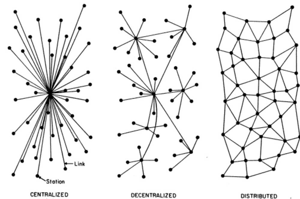
Image by Paul Baran, an early computer network pioneer and one of the two inventors of packet switching.
This famous image of Paul Baran shows the difference between three network typologies; centralized, decentralized and distributed. A mesh network is a distributed network in which each node can connect to any other node in the network. This network typology makes the most resilient of networks. When one or more nodes drop out the network can continue to function. This as opposed to a centralized network in which the central node is a single point of failure. The mesh topology has many benefits. It is resilient. It is hard to censor communications because each node can transfer data to all other nodes in the network. Contrary to a centralized network in which the central node holds all the power, in a mesh network power is equally distributed over all the nodes in the network.
For more on the idea behind post-collapse networking and its use cases, see the description page.
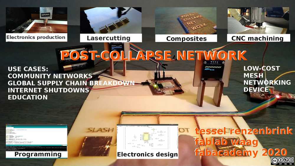
This page provides the information on how to make a post-collapse networking device. It is divided up in segments each explaining how to make one part of the system. At the top of each segment there are links to the most relevant weekly assigment where the design and machining processes are described. Below it are the source files. Followed by a breakdown of the process used.
Link to Vimeo in case the self-hosted video does not work.
Description of the system as a whole
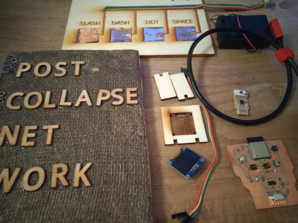
The post-collapse networking system use morse code to communicate between the nodes. It consists of a PCB, a keyboard, an OLED monitor and a manual. The manual explains how to build the device and how to operate the network.
The board is equipped with a ESP32-WROOM chip. The painlessMesh protocol is programmed onto the chip and takes care of the mesh networking. The ESP32 has 10 touchpins, for of these are broken out. A keyboard with four touchpads is connected to the pins. It contains the four characters needed to communicate with morse code: dash, dot, space, slash.
When a message is entered through the keyboard it is both displayed on the monitor and broadcasted over the network to the other nodes.
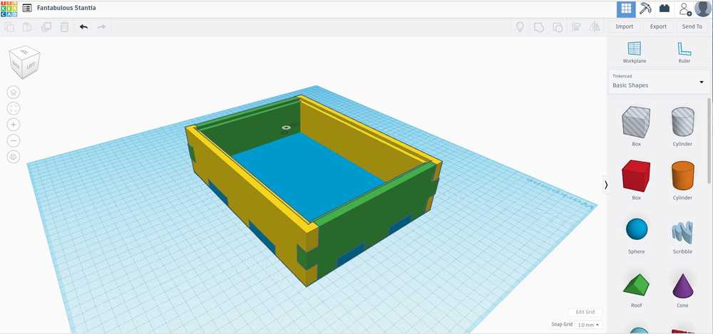
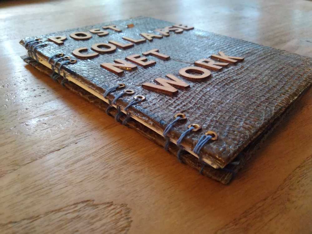
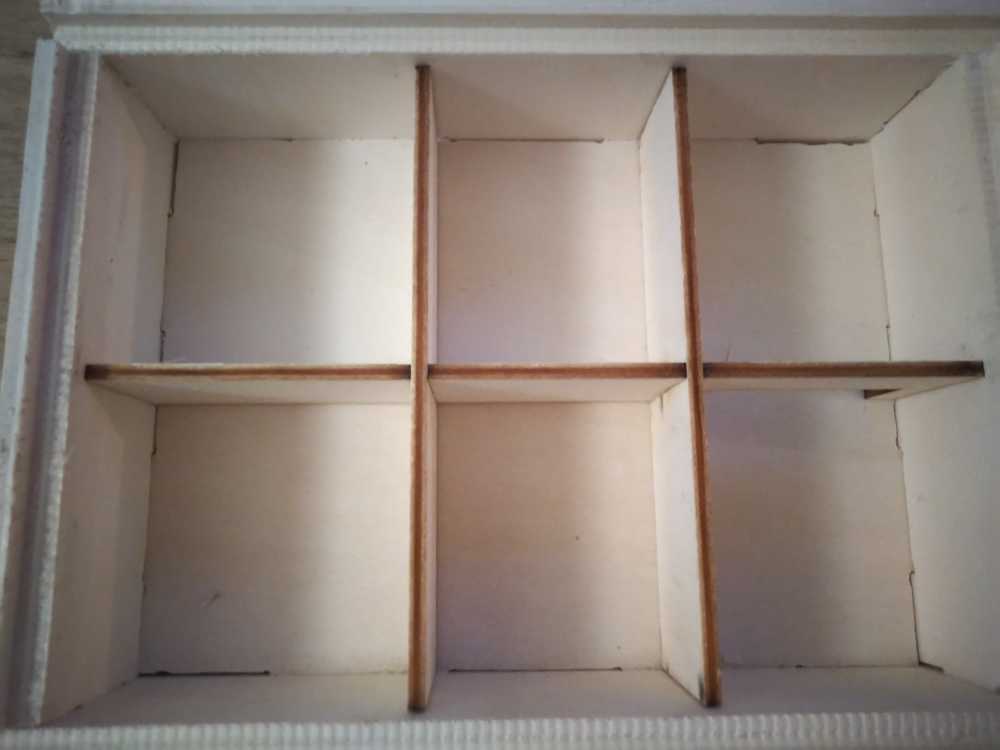
The casing consists of a CNC-ed box which is internally divided in segments. All the parts for the device have a place in the box. From the wires, to the programmer, to the keyboard, to the board. The The box’s lid is a sturdy manual made from composites. When the device is assembled, the electronics are exposed. This has the purpose of making the technology transparant to anybody who is using it. Technology is not a mystical thing that only a few wizards can understand. Anybody and everybody can use, understand and make technology.
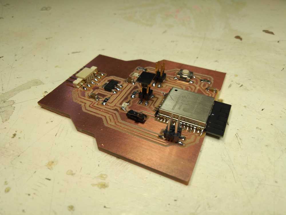
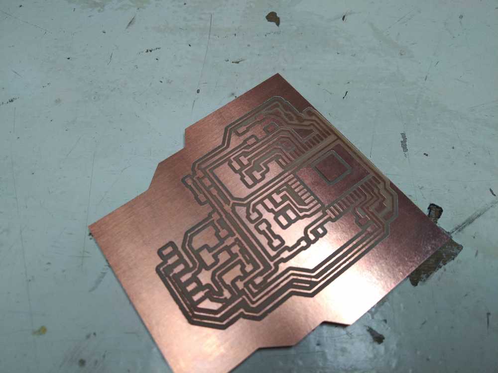
Board
The board is the result of a bunch of iterations of boards with the ESP-module. The ESP series are low-cost Wi-Fi microchips, with a full TCP/IP stack and microcontroller capability, produced by Espressif Systems in Shanghai, China. I made boards with both the earlier ESP8266 module and the later, more powerful ESP32. The board used for my final project has the ESP32 module. The quest for making a working ESP-based board can be found in week14 Networking and communications.
Source files
| Description | link |
|---|---|
| KiCad ESP32 project | Downloadable zip |
| Code for ESP32 using touchpins and painlessMesh | Downloadable zip |
| Design files for keyboard and monitor casing | Downloadable zip |
| Code for ESP32: mesh network, touchpins and oled monitor | Downloadable zip |
Bill of Materials
| component | quantity | price |
|---|---|---|
| ESP-32WROOM | 1 | € 4,57 |
| copper board | 1 | approx. €10,- per 5 pcs = €2 |
| Voltage regulator LM117-3.3 /SOT-223 | 1 | € 0,81 |
| capacitor 10uF | 2 | 2x € 0,03 = € 0,06 |
| capacitor 0.1 uF | 1 | € 0,03 |
| LED green | 2 | 2x € 0,12 = € 0,24 |
| Resistor 100-ohm | 2 | 2x € € 0,21 = € 0,42 |
| Resistor 10k-ohm | 1 | € 0,21 |
| FTDI 6-pin header | 1 | € 0,28 |
| Pin header 2x2 | 3 | 3 x € 0,28 = € 0,76 |
| Slide switch | 1 | € 0,18 |
| Push button | 1 | € 0,27 |
Total cost: € 9.83
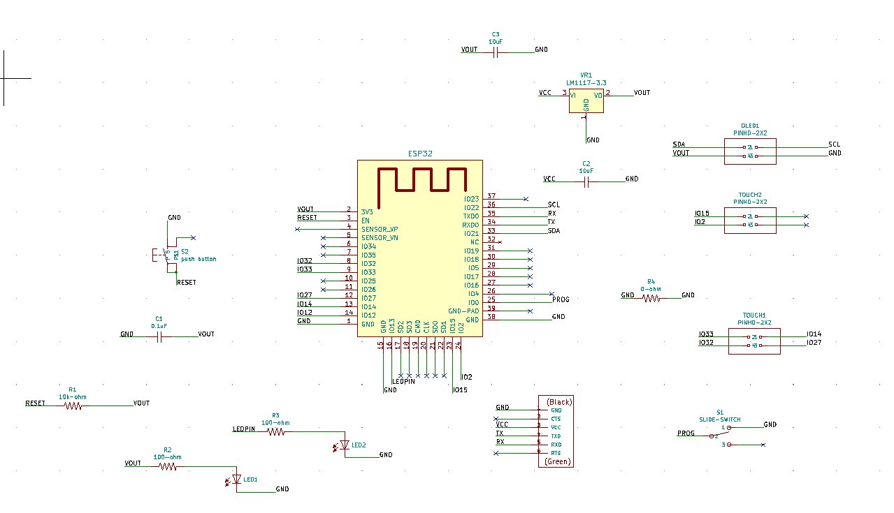
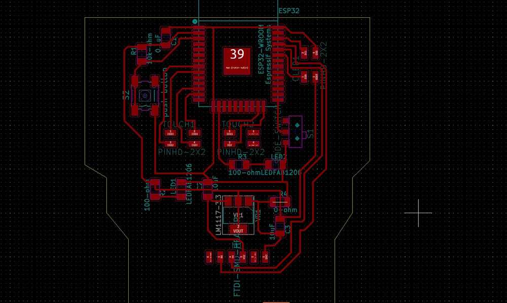
Design
The board was designed in KiCad.
Images of the KiCad design files:
Here is the EEschema:
And here the PCBnew:
Milling and soldering
The board was milled with the Roland Modela MDX-20 small milling machine. Milling and soldering is described in Week04 Electronics production.
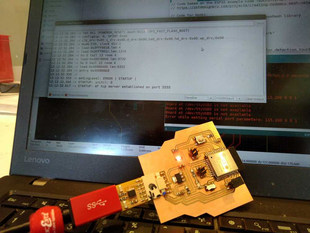
Mesh networking
Crucial to my final project is mesh networking, a network architecture in which all nodes are equal and can all connect to each other. The actively developed painlessMesh library works really well for creating mesh networks.
Board establishing a mesh network:
Code
The painless mesh library is used to create a mesh network. Programming is needed to utilize the touch pins of the ESP32. The the touchpin code had to be combined with the painlessMesh code. When a touch pin is activated it must trigger the event of broadcasting a message to all the nodes in the network. Here is the link to how I got the code to work.
The board is receiving messages from the second node and is outputting touchpin data.
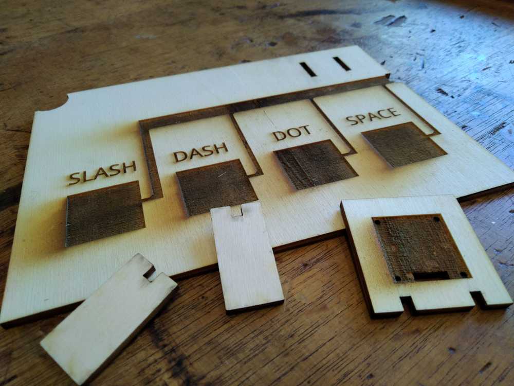
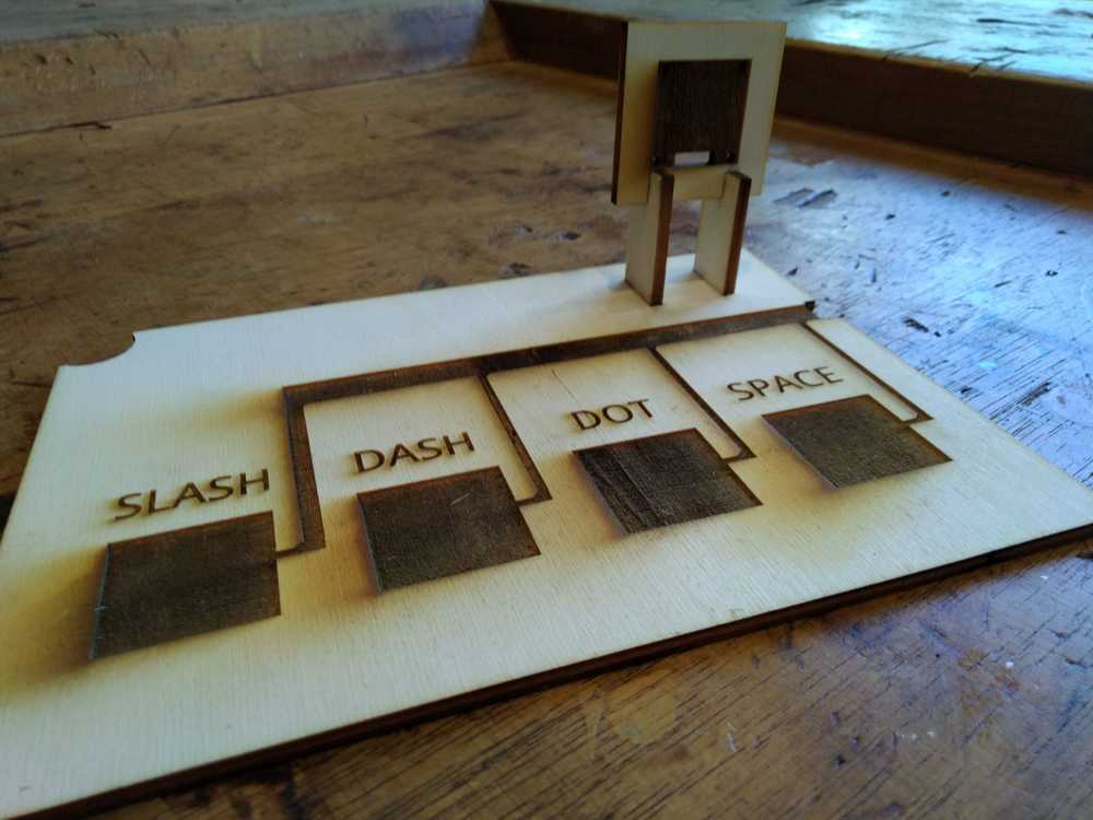
Keyboard
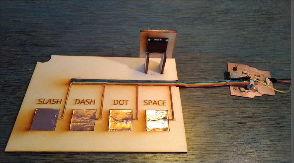
In week09 input devices I made a keyboard. That was a ATtiny44 board turned into a step response sensor. The keyboard for this final assignment makes use of the touch pins of the ESP32 chip. The keyboard has copper pads. When touched they activate the pins on the ESP32.
The keyboard has four input keys: slash, dash, dot, space. These are the four characters needed for sending morse code. The space separates letters and the dash separates words. For instance the code:
.... . .-.. .-.. — / .– — .-. .-.. -.. -.-.–
reads: Hello world!
Here is an online morse code translator.
Processes applied
The keyboard was made with lasercutting, see week03 computer controlled cutting. Engraving was doen with Speed 500 Power 50. Cutting was done at Speed 100 Power 100
Design in KiCad
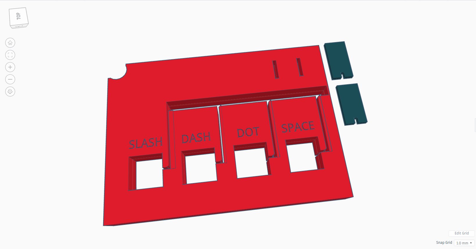
Keyboard.
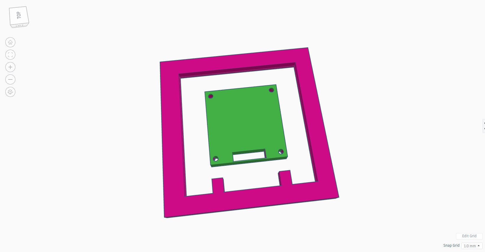
Monitor.
Parts.
Assembled.
Casing
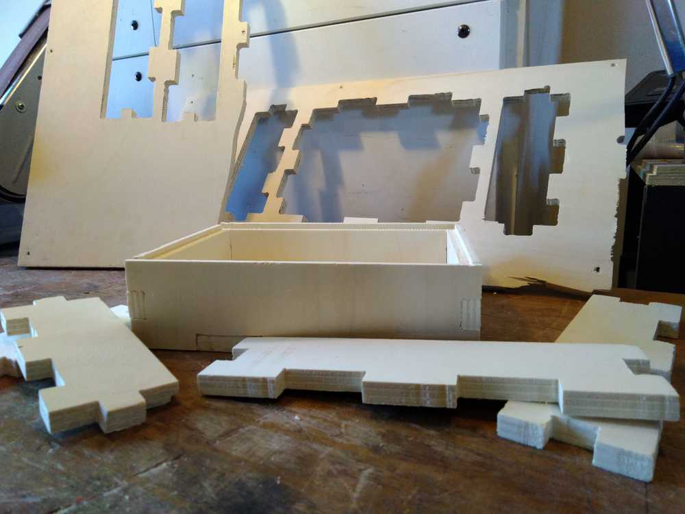
This casing was made with the CNC machine using the 2D milling process described in week07 Computer-controlled machining
Source files
| Description | link |
|---|---|
| Tinkercad design & Inkscape .SVG & .DFX of casing | Downloadable zip |
| Dividers inside the casing | Downloadable zip |
Processes applied
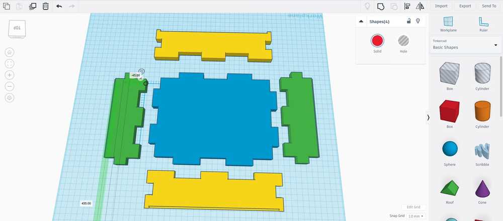
2D design in TinkerCad
Design of the press-fit finger-joint casing using TinkerCad.
Description on how to use TinkerCad in week07 - 3D scanning and printing & week07 - computer-controlled machining. But TinkerCad has basically no learning curve to speak of, it is that easy.
TinkerCad is definitely not the best program for making 2D designs. Its primary function is for designing files for 3D printing. The program I primarily used for 2D design during FabAcademy was FreeCad. However, FreeCad demands a Zen-like state of being-in-the-world. As with Zen, you must accept that there is a logic behind it all, but that that logic will never be revealed to you. As with Zen you must accept nothing is permanent. A system crash can obliterate your work in an instant. As with Zen you must learn to live with your mistakes. CTRL-Z, the blessing of the computer age, is not available to those venturing into FreeCad. What I learned about myself is that my being-in-the-world is nowhere near Zen-like. Nearing the end of FabAcademy I snapped and took a vow never to use FreeCad again. Since Fusion360 is not available for my Linux computer these designs are made in TinkerCad.
Preparing files in Inkscape
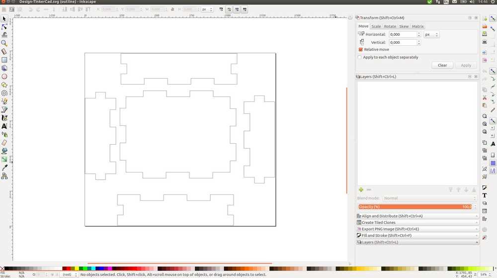
Description on how to use Inkscape in week 02 - Computer-aided design & week 03 - computer-controlled cutting
The SVG file can’t be loaded into V-Carve, the software to prepare designs for the milling machine. You need to convert them into an .DXF file. For this I used Inkscape.
2D milling on CNC machine
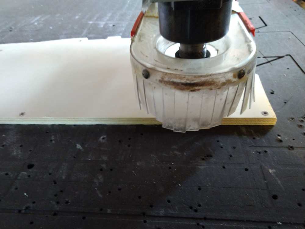
To mill anything you need to use the V-Carve program to prepare your design. You need the Shopbot software to operate the CNC-machine and you need to know how to operate the CNC-machine and how to use it safely. All this is described in Computer-controlled machining. Here I’ll just describe the settings I used in V-Carve:
Pocket toolpath:
Two flute end mill with a diameter of 3mm.
Cutting parameters: Pass depth 1.5mm; steppover 1.8mm at 60%.
Spindle speed: 18.000 rpm.
Feed rate: 80 mm/sec; plunge rate 80 mm/sec.
Cut depth 5mm.
Clear pocket: raster.
Cutting toolpath:
Two flute end mill with a diameter of 3mm.
Cutting parameters: Pass depth 1.5mm; steppover 1.8mm at 60%.
Spindle speed: 18.000 rpm.
Feed rate: 80 mm/sec; plunge rate 80 mm/sec.
Cut depth 13.3mm.
Machine vector: outside/right
Last pass: no.
Added tabs at 200mm intervals with a 2mm thickness.
And added dogbones of 1.5mm.
After the CNC machine had milled the wood, I sanded of about a millimeter to make it press fit.
Dividers
The dividers on the inside of the casing are made with the lasercutter.
Book
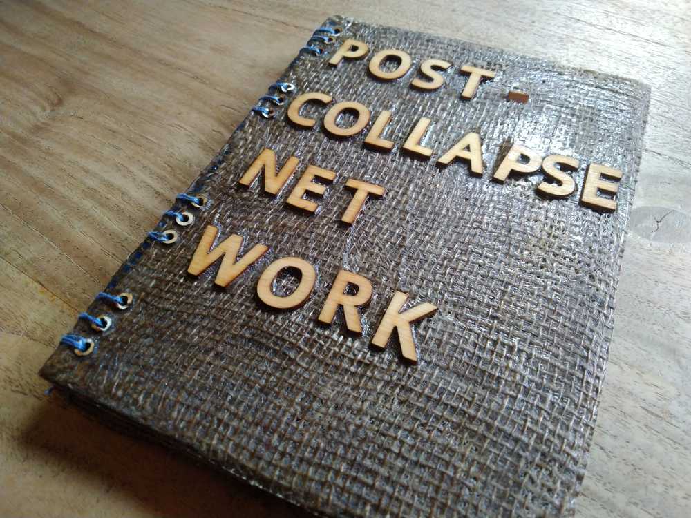
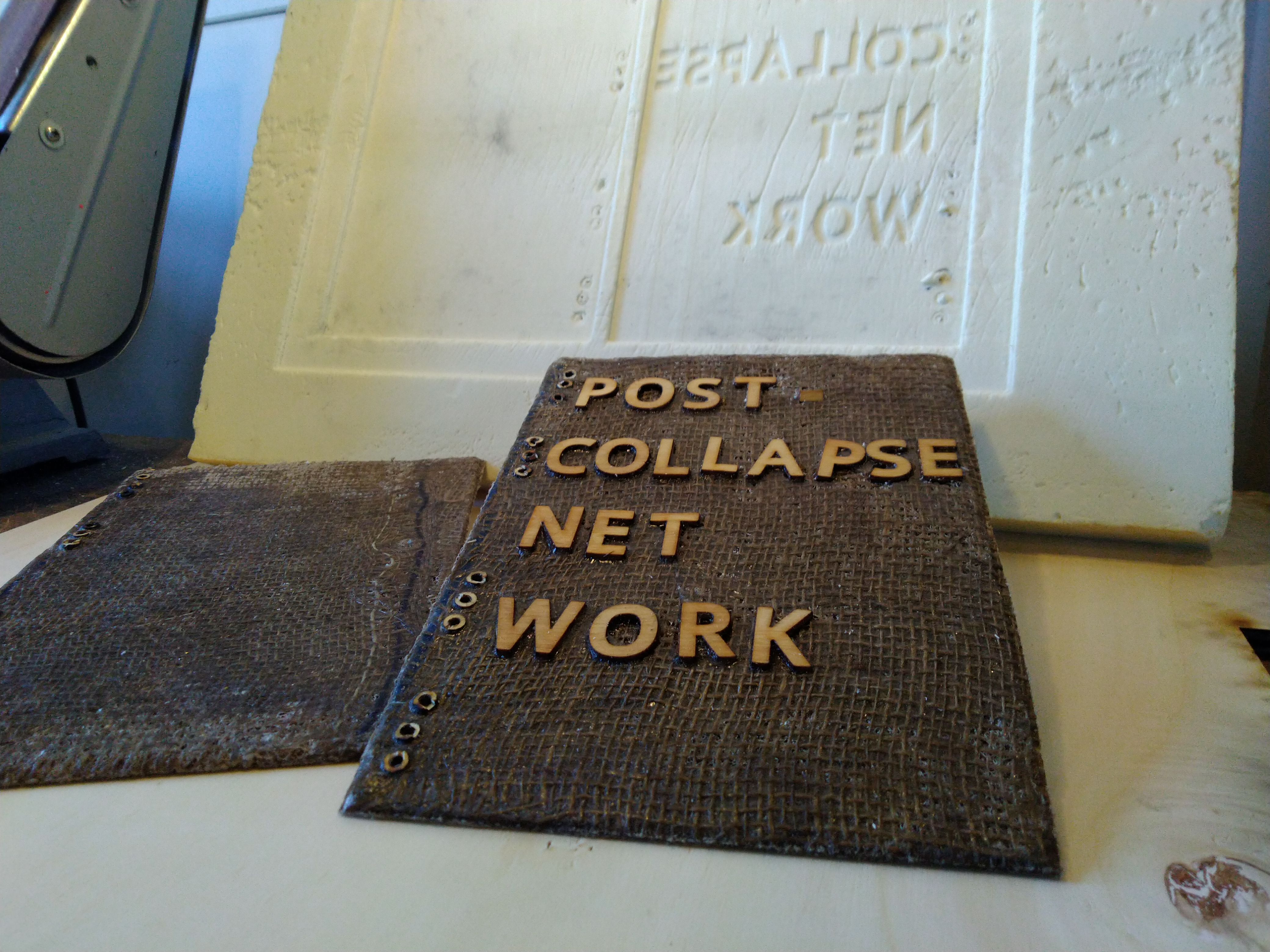
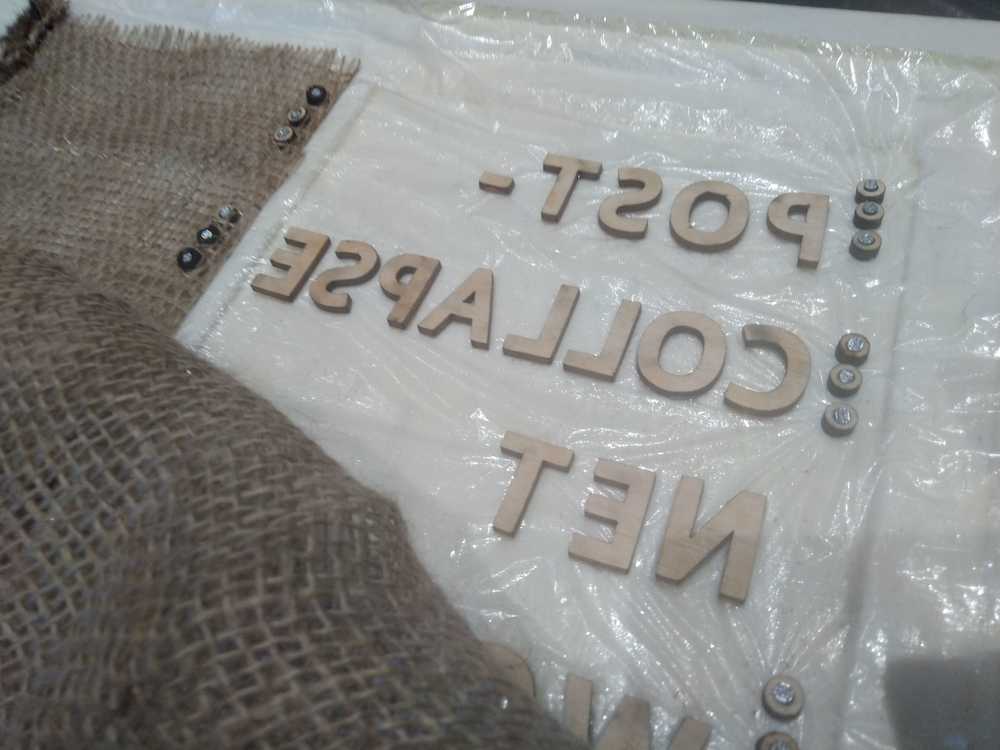
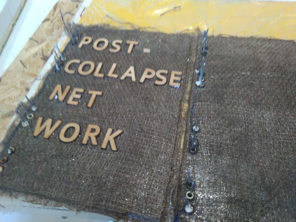
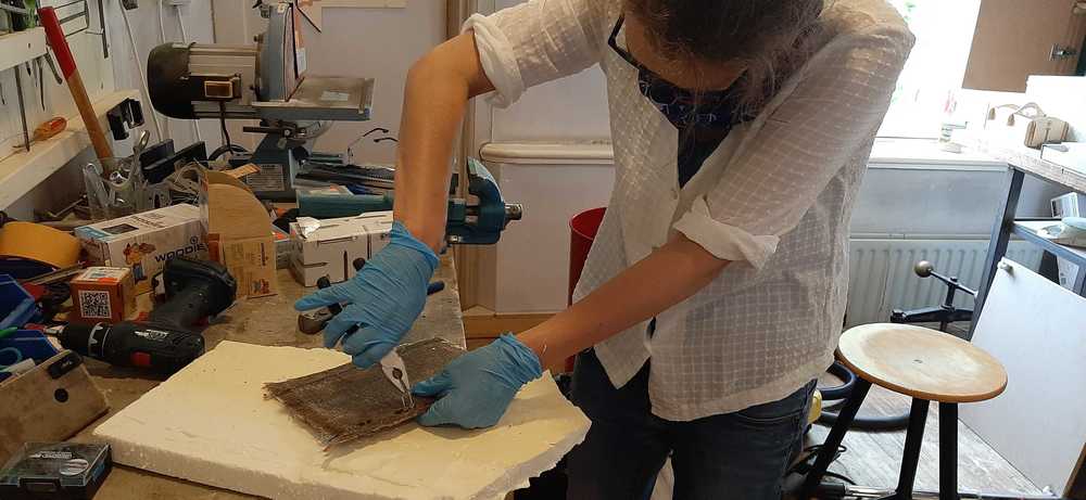
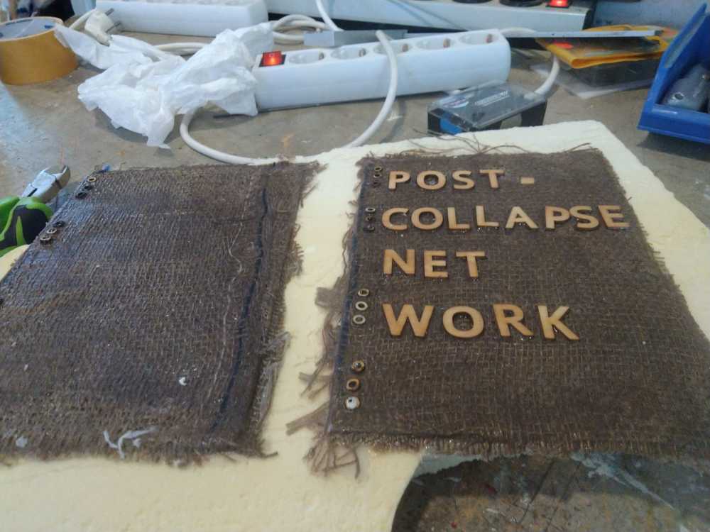
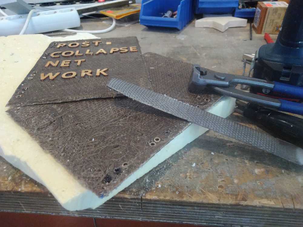
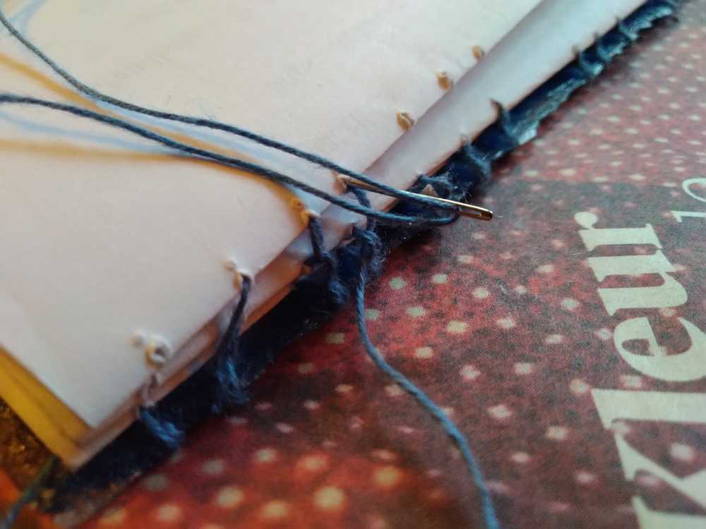
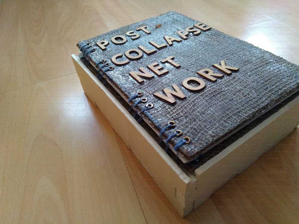
The book cover was made with composites. The process of making the entire book is described in week16 Wild card week. For composites you make a mold in foam using 3D milling. Next you fill the mold with textiles drenched in expoy. Clamp the mold tied and let it harden. I made letters with the lasercutter to have an embossed title on the cover. The letters fit into a clearing that was made in the design. That keeps them from moving out of place during the hardening process. I also lasercutted rings to make holes in the side of the cover. These holes are used to stitch the book cover and the paper pages together with a book binding process called coptic stitching.
Source files
| Description | link |
|---|---|
| Tinkercad design of book cover | Downloadable zip |
| Inkscape .SVG and .DXF of letters for the lasercutter | Downloadable zip |
| Inkscape .SVG and .DXF of the rings for the lasercutter | Downloadable zip |
Processes applied
3D design in TinkerCad
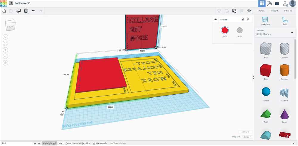
3D milling on CNC machine
For an extensive description on the process of 3D milling see week15 Molding and casting and week16 Wild card week. Here I’ll just describe the settings I used in V-Carve:
For the roughing toolpath I used a two flute end mill with a diameter of 3mm.
Cutting parameters: Pass depth 1.5mm; steppover 1.5mm at 50%.
Spindle speed: 10.000 rpm.
Feed rate: 120 mm/sec; plunge rate 120 mm/sec.
Model Boundery.
Machining allowance 0.5mm.
Rouching strategy: Raster X.
For the finishing toolpath I used a two flute end mill with a diameter of 3mm.
Cutting parameters: Pass depth 1.5mm; steppover 1.5mm at 50%.
Spindle speed: 10.000 rpm.
Feed rate: 120 mm/sec; plunge rate 120 mm/sec.
Model Boundery.
Machining allowance 0.5mm.
Rouching strategy: Raster.
Lasercutting
I lasercutted the letters and rings from 5mm thick wood. The settings I used for the lasercutter are: speed 25, power 100.
Composites
I used jute as the textile and epoxy to make the composite.
 I covered the mold in cling foil covered in vasiline. I then placed the lasercutted letters in the pockets made for them on the CNC machine. I placed the rings on the side of both covers. I used nails to keep them in place. I covered the top of the nails in vasiline too. Then I drenched the jute in epoxy and placed it inside the mold.
This is how the mold came out.
The nails came out with some wriggling.
There was some epoxy drenched jute hardened outside of the mold.
I removed it with a file and pincers.
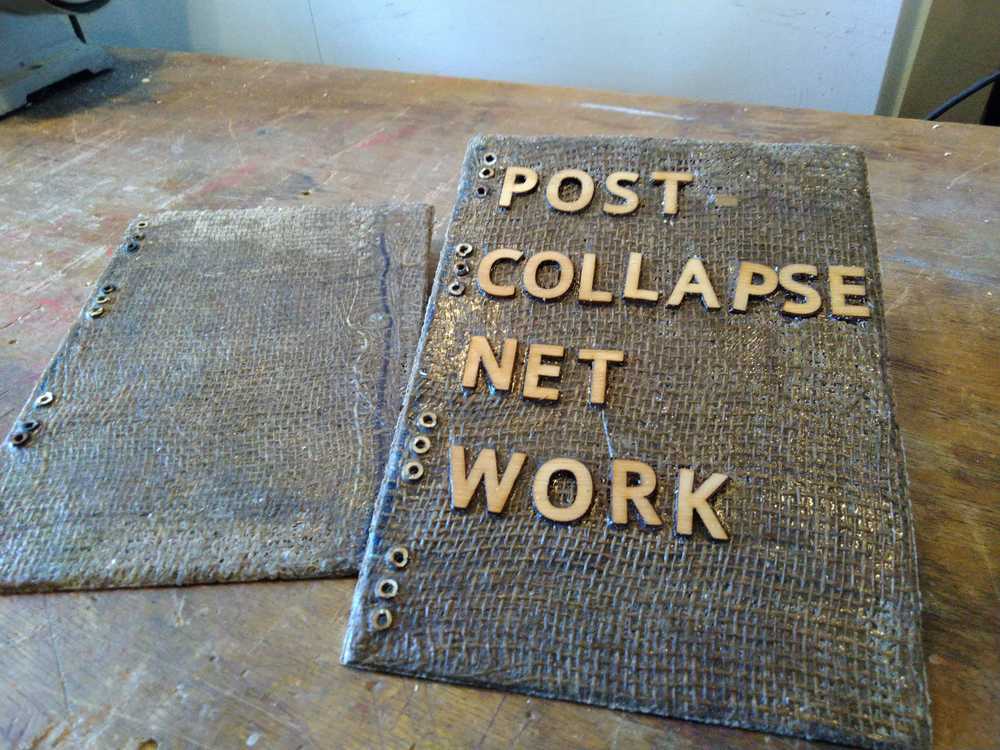
This is how the covers came out.
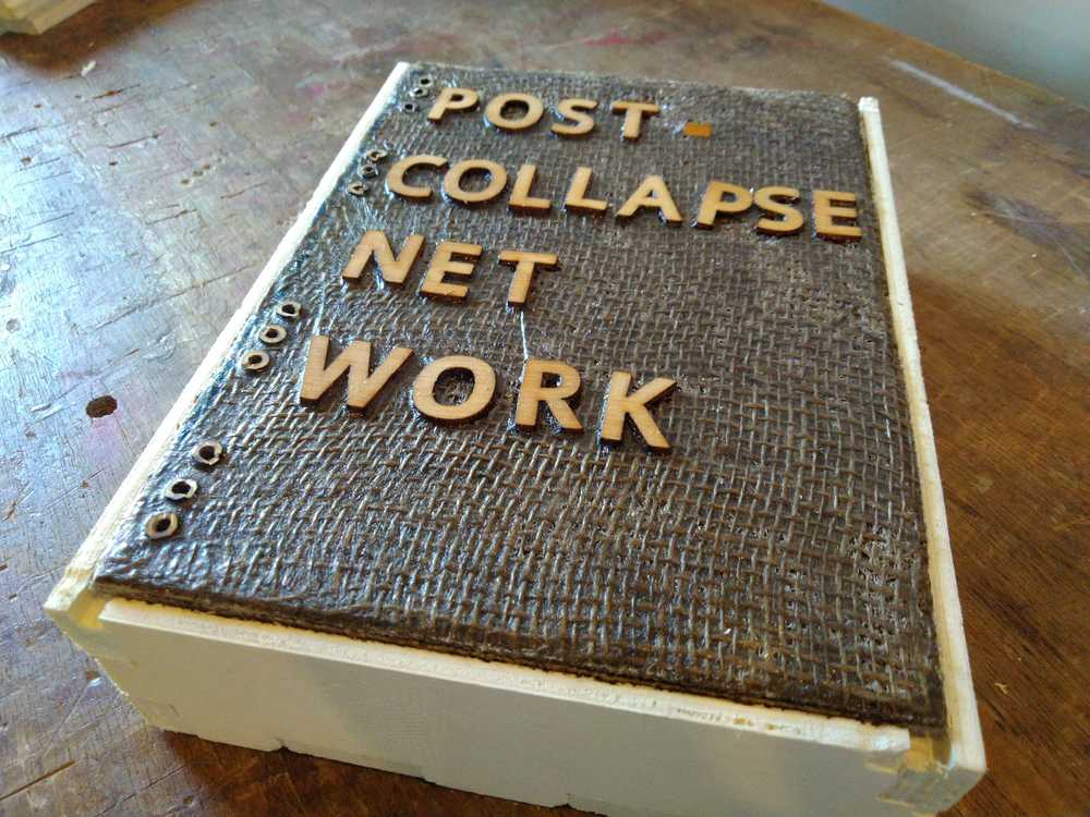
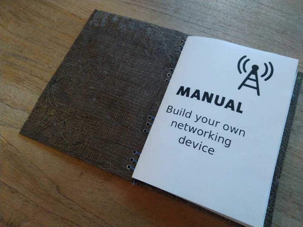
The book is both a manual to the machine and serves as a lid for the casing.
Book binding
I used coptic stitching to bind the book. A step by step explanation on how to do it is provided in week16.
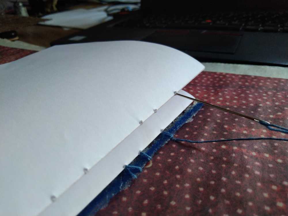 In short: you fold the pages into signatures: bundles of 8 double folded papers. Then you use a special stitching technique to stitch the book covers and signatures together.
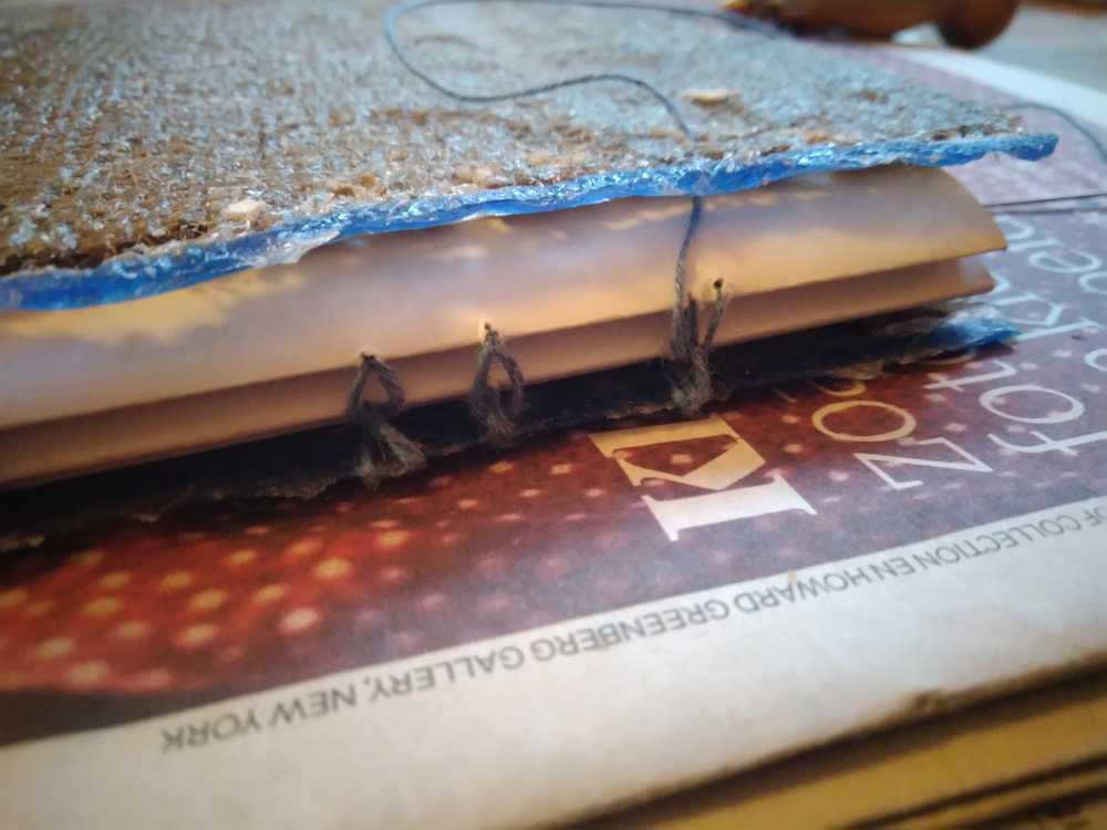
Book after stitching it up:
The book is a manual explaining how to make your own networking device.
Book as lid of the casing.
Video
Credits for the video:
Voice over: Filip Mertens
Music: Ambiant Konnekt - Citrus. Sirona records. CC licence: BY-NC-SA 3.0. Hosted at archive.org.
The post-collapse network was made by: Tessel Renzenbrink
At: Fablab Waag
FabAcademy 2020
Slide
Slide with the description of the project and pictures of the processes used.
Final words
FabAcademy is fantastic and horrible. It’s fantastic to learn so much in a short period of time. And it was fantastic to be on this journey with my class mates Hyejin, Nathan, Harm and Rinke and our mentors Henk and Rutger. There is something intensily satisfying about concentrating on a single thing for an extended period of time. For five months my life was just about learning new skills and pushing myself to finish the weekly projects. But crash learning is like a mountainous path. There are many highs but also many lows. It is of course very satisfying when you finish a project applying skills you did not have only one week ago. But it’s also hard to spend a day figuring out why your device is not showing up on your USB port as the Wednesday deadline is rushing toward you.
The hardest part of FabAcademy was the feeling that I was neglecting every other aspect of my life. The people around me, the plants in my garden, thoughts about something other than that week’s assignment, it feels like a pushed all those things to the periphery as I focused on a single task.
But now that it is over it is of course easy to say that it was all worth it. I have learned so much. The hands-on skills, but also the mindset that you can make and do (almost) anything yourself. Not by yourself, though. For it is clear that doing things together yields much better results and is so so so so so much more fun.
So thank you Nathan, Harm, Hyejin, Henk and Rutger. Our regional collaboration labs Agrilab and ULB. Professor Neil Gershenfeld, the man who knows (almost) everything. Our global reviewer Yuichi Tamiya. And everybody from the FabLab network. It was a great journey. I hope it will not end.
Pandemic
FabAcademy 2020 was special in that the world got hit by the COVID-19 pandemic. Most labs were closed for at least a part of the course due to lockdowns in response to the breakout. At the very start of this journey, I’ve said that I was drawn to the Fab network because of five principles: know your tech, hyperlocal fabrication, distributed learning, open & sharing and reducing building blocks. During the COVID-19 pandemic these principles were put to the test. And they proved to be more than just ideals. FabLabs all over the world harnessed their machines, their knowledge and the global network of people to contribute to the fight against the virus. Labs fabricated protective gear for medical personel, kept improving the designs and shared them globally. As global supply chains faltered the importance of local fabrication became very clear. The Fab network collaborated globally to provide relieve locally. The creative, problem solving mindset combined with the distributed approach provided a useful contribution to the more centralized approach of governments and large companies in battling the pandemic.
More specifically about the FabAcademy, it proved to be better prepared for a sudden shift to online collaboration than most educational institutions. Being a distributed learning platform utilizing online tools like videoconferencing and GitLab, the infrastructure for remote education was already in place. Also, FabAcademy doesn’t teach you what you should know, but teaches you how to learn what you want to know. This emphasis on self-education contributed to us students being able to continue even though we could not go to the lab.
Here in the Netherlands the government imposed an ‘intelligent lockdown’. People were urged to stay at home and we did not go to the lab for seven weeks. But thanks to the FabAcademy and with special thanks to our mentor Henk we were able to continue. Henk kept us going by providing electronics kits so we could tinker at home. He managed multiple communication tools like Jitsi and Slack so we could go on collaborating. He was always available online for questions. To give an idea of the extent of moving our learning and collaboration online: we did seven group assignments remotely and we did them all succesfully.
Nevertheless, the FabAcademy is a hands-on and a collaborative course. The first time we were allowed back into the lab I felt such a joy of working together again. I had not realized what I had missed until we got it back again.
For me the hardest part of learning remotely is motivation. We did all the electronics assignments during the lockdown because these can be done from home. But electronics involves a lot of slamming your head against a wall. Something does not work and you spend hours trying to figure out why. When you are in the lab, you can share your frustration with your fellow students and they’ll tell you it’s the same for them. And then you can laugh about it. And you can shoot a quick question to your mentor who - if he does not tell you to read the datasheet - saves you hours of fruitless searching on the internet.
The lockdown taught us that we can do it remotely if we must. But that it is so much better to do things together.
Global review
For the global review of the documentation more information was asked which I will place here.
One question is: what elements did you use for your project. Place all the elements on a flat surface.
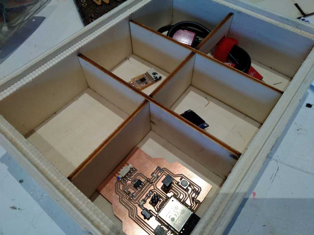
 Here is the CNCed casing that serves as a kit that contains all the components.
Here are the components that are in the CNCed box.
 In the left lower corner the post-collapse network manual.
Above it the keyboard. It has a ribbon cable running off it. This connects to the pinheader connected to the touchpins of the board.
To the keyboard’s right is the battery holder.
Next to it is a USB cable. This is used to connect the FTDI to the USB port in your computer.
In the circle of the cable is the FTDI. This is added to the kit so people can program the post-collapse networking device.
The rainbow colored ribbon cable is used to connect the OLED monitor to the board.
Next to it are three lasercutted components that serve to mount the OLED monitor on the keyboard.
Below the lasercutted components lies the OLED monitor.
To its right is the post-collapse networking board, the PCB I designed, milled, soldered and programmed.
I’ve made a new slide with a larger font and an added creative commonse licence mark.
I was asked about the other boards in the video. The video features four boards in total. A NodeMCU, an Adafruit Feather, the Barduino development board and my own board.
In week14 Networking and communications I explain how each of these boards feature in my learning to make and program my final own board: the post-collapse networking device. It is that device that is my final project. The off-the-shelf NodeMCU and Feather aren’t part of my final project and neither is the Barduino. I learned a lot from making the Barduino and it is a great development board. But in the end you want to make your own board, because making boards is really really cool. Also, for the final project, making your own board is a hard requirement. See the final project requirements page.
However, it is allowed to use commercial boards and/or development boards like the Barduino as extra nodes in a network according to the Commercial Board Policy. It states about such boards that: “These can be used as a extra nodes of a network that you have built, with the purpose of showing the network functionality of one of your fabricated boards.”
I have made a mesh networking device. To show what it does it must have other nodes to network with. That is where the three other boards come in. At the beginning of the video on the 13 second mark, I show how the boards are programmed to blink their LEDs in short succesive bursts for the number of nodes in the network. The more nodes, the cooler the effect. That is why I used all four networking capable boards I had to make that shot for the video.
On the 55 second mark of the video I show multiple functionalities of the board I designed.
- My board is connected to the keyboard. When you type on the keyboard, the characters are displayed on the OLED monitor that is connected to my board.
- A second functionality is that when a character is typed on the keyboard, it is broadcasted to the rest of the network by my board. To make this function visible a second node connected to a second monitor was needed. This role is played by the Barduino.
For purposes of the video I made a second copy of the lasercutted keyboard frame. This allowed me to mount the OLED monitor and place clearly visible in the shot of the camera. It is not part of my final project as such. It is only there to show how my own board, the keyboard, the oled monitor and the mesh networking, function.
But I understand now that this has led to confusion about which parts in the video are part of my final project and which parts are not. Therefore, I made three new video’s that address the questions raised.
In two of these three new video’s the Barduino will be featured again because I cannot show the networking features of my own board without it. But in the description each video I will clearly state which board is my board and which board is the Barduino.
Here are the issues that were raised for the review. I address them in the video’s below.
- Make a clear distinction between your final project and the secondary nodes.
- Remove all unconnected wires and fold the wires of the battery pack more neatly.
- Don’t show two different keyboards.
- The sending and receiving nodes are too close to eachother. Show them further apart.
For all three video’s goes:
- There are no unconnected wires anymore.
- The battery pack’s wires are neatly packed together.
- No use of extra keyboards for composition purposes.
Note that unfortunately the OLED display has deteriorated since I made the final video for the presentation. I pressed it too hard a couple of days ago and since then the display shows the characters a lot less sharp.
Video 1 addresses the following issue: The sending and the receiving node are too close to eachother.
In this video the sending and receiving node are on two different tables. The camera starts on my board and displays that messages are received. The board is powered by a battery pack.
Then it pans to another table where the Barduino is on. The Barduino is connected to a USB port to draw power.
The OLED monitor displays the ‘hello from node [IDnumber]’ message.
Video 2 addresses the issue of which parts belong to my final project. In this video only my own board is visible. It is running on a battery pack. It shows that when the touchpads are touched, the character is displayed on the OLED monitor.
Video 3 show that my board can receive messages from other nodes and display them on the monitor. The video opens with a shot of the Barduino. The Barduino only serves as a second node in the network to show networking capabilities. It is not part of my final project. The Barduino is shown to be connected to the USB port for power supply.
The camera then pans to my board and shows it connected to the keyboard and OLED monitor. It is powered by a battery pack.
The camera then closes in on the OLED monitor and shows how it is receiving a message from the other node. The OLED monitor displays the ‘hello from node [IDnumber]’ message.
What the final project is and how it works
Another issue with the documentation, is that there is not enough information on what my final project is and what it does. I have added extra information here.
Final Project - Description
Final outcome
A post-collapse information and communication networking device built from a minimal amount of building blocks so that it is affordable and accessible to all people. It is easy to use and easy to build should you want to learn how communication networks work.
Goal
There are many community networks in the world such as Guifi.net in Catalonia and SNET (Street Network) in Cuba. Their beauty is that they can and do operate without corporate or State ISPs. The open architecture of networking protocols such as TCP/IP make it possible to operate a network completely independent from any outside party.
But for hardware it’s different. The physical part of communication networks relies on the global supply chain. Which means that if supply is disrupted - for whatever reason - building and maintaining networks becomes harder.
I have build a networked communication device using the least possible physical means. This ties in with the aim of the FabLab community to minimize the input building blocks into FabLabs. (This was discussed in the global lecture of week 01).
Requirements
I use WiFi capable chip to establish a device that is capable of wireless communication. I use the mesh networking protocol painlessMesh to establish a mesh network between WiFi capable devices. The name post-collapse networking device refers to the imagined situation for which this device is intended. A situation in which the established communication networks no longer work. In this scenario people can build their own devices from few components that are low cost. The idea is that this network is used only for the most important of communications.
It does not seek to rebuild an internet with a lot of bandwidth and storage space. A surplus that has let to much unnessecary communication, like pictures of cats and petabytes of home made videos.
The post-collapse network goes back to the bare minimum. In a way it seeks to emulate the early days of the old internet. Where lack of resources made people truly think about what they would send over the network before sending it. As one early internet pioneer described it: they would send each other e-mails or leave messages on the bulletin boards. Sending and receiving was so slow in those days that it could take days for a message to arrive. Storage space was so scarce that they only wrote the essential stuff. No pictures and certainly no videos. This early pioneer said about that type of communcation: “you thought really hard about what you would write because there were such long intervals between writing and receiving. You would write your text, edit and re-edit it before sending it. Since communication was so scarce we only send the best part of ourselves over the net.” (I cannot link to this conversation because it was a conversation that took place without any recording devices around us and there is no record of it on the internet). I also no longer remember the name of this person. But I remember something better than his name: the meaning he conveyed.
This type of scarcity of communication appeals to me. As the anecdote above seeks to convey: it makes us consider what we say, rather than just posting every thought online that comes to our mind. This is why I like the idea of using morse code for communication in this project. It takes effort to learn morse code. It takes time to enter morse code and it takes time to decipher morse code. All of this throws up a barrier for communication. And therefore people will give thought to what they will send over the network.
The idea of the post-collapse network is that it serves as a tool to transmit the most essential communication.
On post-collapse
I use the short-hand ‘post-collapse’ to refer to the situation in which a minimal building block, low-cost network will be of use. This term is not to be understood as a term that refers to a singular event or possible future in which the global economy has collapsed. William Gibson has said: “The future is already here. It’s just unevenly distributed”. In our world many ‘futuristic’ realities currently exist in parallel.
There currently are localities on earth where hardware availablity isn’t as plentiful as where I live. There are political contexts that call for sovereign networks. For me personally, seeing the rapid rise of surveillance capitalism makes me interested in technology sovereignity in order to conceive of and create alternative technological realities.
Pandemic
Oddly, the post-collapse reality has caught up with most of the world since I conceived of this project. The Covid-19 virus has hugely disrupted the global supply chain. The electronics industry is hit hard especially. Much of the stock for electronics production is produced in one locallity: China. When Covid-19 forced productivity and shipping to a hold there, the electronics industry was confronted with this single point of failure.
Another relevant observation is the enormous reliance on the internet during this pandemic. Much of public live in the Netherlands, much of Europe and many many countries in the world grinded to a hold. Regimes of social distancing and lock downs resulted in closed schools, stores, pubs, sports clubs and places of work. People were advised against or even prohibited from meeting each other. Instantly, much of social, educational and work-related interactions moved to online environments. Although the streets were empty we could still interact with each other. Through video conferencing, text messages, VOIP and email, we could keep in contact. The internet had become a life line, the primary channel for human interaction. All this to say that communication technologies are essential during a break down of the status quo. And that this project’s goal to make communication devices from the most minimal of building blocks, so that they can be manufactured under many circumstances seems all the more relevant to me now.
The post-collapse networking device is conceived for a situation in which people are suddenly confronted with the need to build their own communication network. People may not be prepared for this. They may have no knowledge of networking or electronics at all. Therefore part of the device’s kit is a manual that explains how to build the device and how to operate a network.
Context of the project:
The aim of this project is to make devices capable of forming a DIY autonomous internet.
The internet, or interconnected networks, is a marvelous invention. Instant communication and data exchange has increased humanity’s capability to collaborate, swap ideas and build on one another’s work. But despite the heavy reliance on communication networking, most people do not know how to build and operate a communication network. For most people, the global internet ‘just works’. As such they are entirely dependent on companies and institutions and the hardware infrastructure they provide for their digital communication.
There are many conceivable situations wherein access to an open, uncensored internet is restricted or not possible at all:
- remote communities can be underserved because it is not profitable for Internet Service Providers to invest in the necessary infrastructure.
- Politically motivated partial or total internet shutdowns like the partial shutdown by the Spanish central government during the Catalonian referendum on independence.
- An internet controlled by large corporations and governments to surveil and control citizens. Captured by the term Surveillance Capitalism, internet usage comes at the price of loss of privacy, autonomy and self-determination.
Hardware scarcity can also be a cause for lack of access.
- The S-network in Cuba, for instance, is completely build on clandestine hardware because importing communication hardware is against the law.
- ICT hardware depends heavily on global supply chains. This project takes into account the possibility of lack of access to those. This is already the case in certain regions on the planet. For political reasons such as the Cuba example, or because of lack of monetary resources.
- Hardware scarcity will affect far more places in the world if the global supply chains collapse. The coronavirus crisis makes clear that dependence on only a few places of manufacturing is a proposition that makes everyone vulnerable. This has become a reality during the coronacrises. The electronics industry was severely hit by the disruption of the global supply chains.
Aim of the project
Assumption
This project assumes that access to the worldwide communication network we call the internet is not possible. Either because access is denied or because off-the-shelf communication devices are not available due to hardware scarcity.
Aim
The aim of the project is to be able to build a community network that can operate autonomously.
That means:
1. Be able to build networking hardware devices with as simple building blocks as possible.
2. Be able to understand how communication networks work and able to operate them.
Requirements based on the assumption above:
Autonomous network
- It does not rely on third parties for providing the backbone infrastructure.
- It does not rely on a central authority that grants of refuses access to the network. It will be a distributed network.
Hardware scarcity
- Using the most simple building blocks as possible.
Technical requirements:
- The network must allow for a-synchronous communication.
- It must allow for many-to-many communication.
- It must be able to run or interoperate with the TCP/IP protocol suite.
- It must be wireless so as not to be dependent on a wired infrastructure. (In case you are not allowed to run cables where ever you please, such as in my country where you will need a permit for that.)
Understandibilty
- An easy-to-use manual must be provided on how to build the device and operate the network.
Describe what your project does
a. Design low-cost, easy-to-make networking devices for post-collapse situations
Build networking devices that enables people to transmit and receive light weight data files.
Considering:
- capabilities: primary use is exchange of text-based communication. Therefore data transfer capability does not have to be large files. Speed is also not an issue. The internet in the ‘80’s could take a day to deliver your message, it only makes you think better about what you want to communicate.
- Handle TCP/IP protocols in order to connect to any internet device.
- Mesh networking.
- Function on a part of the electromagnetic spectrum that is not restricted.
- Using as simple building blocks as possible, in case unlimited access to the global supply chain ceases.
- stretch goal: have it run on its own power: solar panels, mechanically produced electricity by muscle power.
The purpose is to make a device that can easily be made because:
- It has been stripped of complexity and therefore more easy to understand.
- It comes with a easy to read manual that lets you reproduce the device.
- Makes use of simple building blocks that can either be made yourself or scavenged.
Out of scope:
The focus of this project is more to make as simple a device as possible in terms of building blocks than it is to make a versatile device. The context is a post-collapse situation in which you are just happy to have any networking device. The aim is to make it easy to make from components that are readily available. Functionalities like large file transfer, or high speed delivery are outside the scope of this project.
b. A comprehensive manual
A comprehensive guide will be provided explaining how to build the device and how to operate the network. The manual will be digitally available of course. But it will also be published in a book I made myself during wildcard week. The manual/book is part of the packaging of the device. It serves as the lid of the casing. This reduces the chance of loosing the manual.
How the project works
I’ve made a mesh networking device. This is a device that can communicate to other devices and form a network. A network consists of different nodes. In a network of communication devices it is not necessarily so that each node in the network can communicate with any other node in the network. But I have implemented the mesh topology and this enables any node in the network to exchange data with any other node in the network.
To implement mesh networking for my device I used the painlessMesh library. Here is the GitLab home of painlessMesh. This library takes care of mesh networking. The developers of painlessMesh describe it as: “painlessMesh is a true ad-hoc network, meaning that no-planning, central controller, or router is required. Any system of 1 or more nodes will self-organize into fully functional mesh.”
painlessMesh is compatible with the Arduino IDE and can be used by installing the library. Sketch > Include library > manage libraries search for painless mesh. It’ll tell you additional libraries need to be installed. Install all. I had to add the ESPAsynTCP.h library by adding library by zip. Be aware that there are different libraries AsyncTCP libraries for the ESP8266 and the ESP32. The ESP32 will not work with the AsyncTCP library of the ESP8266. But the two different libraries have the same name. For a description on how to solve this see my description in week14.
There are two important notes to make on the use of the painlessMesh library:
1. PainlessMesh uses JSON to handle data transfer. Important to know is that you can’t use the delay function in your code because that will disrupt the mesh networking processes.
2. For all PainlessMesh code the WiFi credentials must be the same for all nodes in the network. The standard WiFi credentials in all the example code is like this.
#define   MESH_PREFIX     "whateverYouLike"
#define   MESH_PASSWORD   "somethingSneaky"
#define   MESH_PORT       5555
The post-collapse networking system uses morse code to communicate between the nodes. Morse code uses four characters to communicate: dash, dot space and slash. Using morse code rather than the alphabet makes for a very different keyboard layout, of course. Using the alphabet you would need at least 28 input keys: the 26 letters of the alphabet and a space and and a dot to indicate the end of words and sentences. But for morse code the keyboard only needs four input keys.
In the code however it is different. Transmitting the characters for the morse code works exactly the same as if they were any other character.
This is implemented in the code as follows:
if(touch1detected){
    touch1detected = false;
    checkDisplay();
    Serial.println("Touch 1 detected");
    display.print("/");
    display.display();

    sendMessage();   // Broadcasting message
    String msg = "/";
    mesh.sendBroadcast( msg );
What happens in this code is that if touch1detected -that is to say, if the touchpin1 is triggered- than a character is printed to the OLED monitor, in this case a dash display.print("/");. It also broadcasts a message to the network. This message consists of the character defined:
endMessage();   // Broadcasting message
    String msg = "/";
    mesh.sendBroadcast( msg );
Obviously, this procedure can also be done for other characters. You just have to define a different character as the variable.
The keyboard works as follows:
The keyboard is a lasercutted frame. Four squares are covered in copper sheething. It uses step response sensors that work with capacitive sensing. Capacitance is “Capacitance is the ratio of the change in electric charge of a system to the corresponding change in its electric potential.” Source: Wikipedia. Capacitive sensing sensors “utilize the electrical property of capacitance and the change of capacitance based on a change in the electrical field around the active face of the sensor.” Source: Automation-insights.
Each of the four copper squares have a certain capacitance value. When they are touched by a finger (or another object) this value changes. This change triggers an event on the pin to which the copper square is connected by means of a wire. In the code you can define the threshold at which point the touching of the square should trigger an event on the touchpin, like so: int threshold = 17; The higher the variable of the threshold is set, the more sensitive the pin becomes.
The ESP32-WROOM, the chip I used for this project, has dedicated touchpins. But you can turn the pins of any microcontroller into a touchpin as I have shown in week9 in which I made a step response sensor with the ATtiny44.
Here is a schemtic of the pinout of the ESP32-WROOM
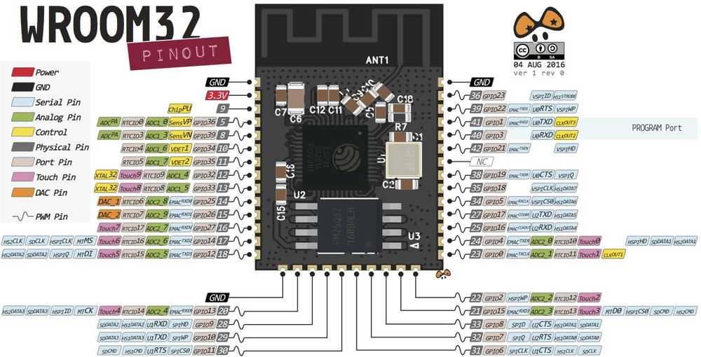
The touchpins are represented in the pink squares as touchx where ‘x’ is the number of the touchpin. The shorthand for touchpin is Tx where ‘x’ is the number of the touchpin. For my board I broke out six touchpins: T6, T7, T8, T9, T2 and T3. These correspond to GPIO14, GPIO27, GPIO33, GPIO32, GPIO2, and GPIO15. GPIO stands for General-Purpose Input/Output and is a way to refer to pins of a microcontroller.
Here is the KiCad schematic in which you can see the pins broken out.
And here is the KiCad PCBnew in which you can see how the touchpins are routed to two 4x2 pinheaders:
.
As described above when discussing the morse code implementation. When a copper pad on the keyboard is touched it triggers an event on the touchpin. In the code I defined that an event on the pin should result in displaying a character on the OLED monitor and broadcasting a message to the network.
The OLED monitor is an I2C device. I2C is an interesting protocol. Here is information about I2C:
- The website i2c.info explains I2C really well:
- ‘I2C is a serial protocol for two-wire interface to connect low-speed devices like microcontrollers, EEPROMs, A/D and D/A converters, I/O interfaces and other similar peripherals in embedded systems. It was invented by Philips and now it is used by almost all major IC manufacturers. Each I2C slave device needs an address – they must still be obtained from NXP (formerly Philips semiconductors).
- ‘I2C bus is popular because it is simple to use, there can be more than one master, only upper bus speed is defined and only two wires with pull-up resistors are needed to connect almost unlimited number of I2C devices. I2C can use even slower microcontrollers with general-purpose I/O pins since they only need to generate correct Start and Stop conditions in addition to functions for reading and writing a byte.
- ‘Each slave device has a unique address. Transfer from and to master device is serial and it is split into 8-bit packets. All these simple requirements make it very simple to implement I2C interface even with cheap microcontrollers that have no special I2C hardware controller. You only need 2 free I/O pins and few simple i2C routines to send and receive commands.
- I2C interface:
I2C uses only two wires: SCL (serial clock) and SDA (serial data). Both need to be pulled up with a resistor to +Vdd. There are also I2C level shifters which can be used to connect to two I2C buses with different voltages. 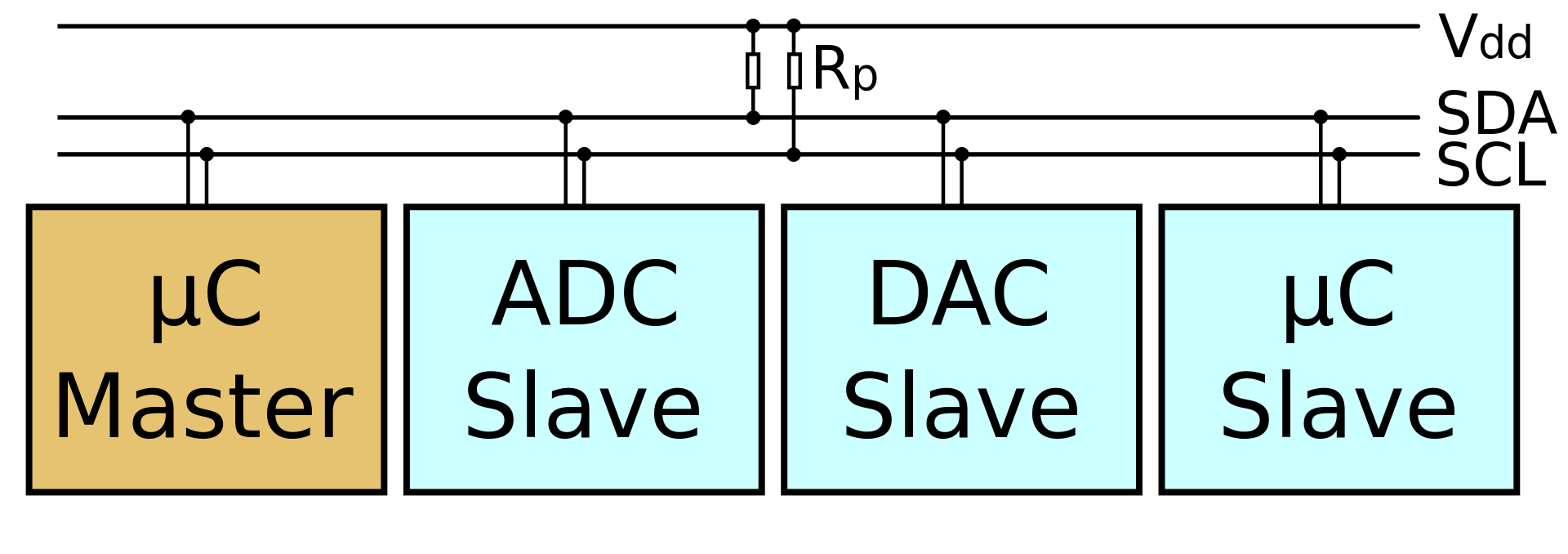
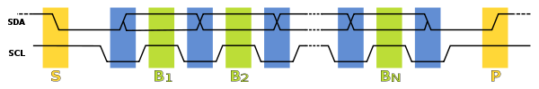
- I2C schema. Source Wikipedia. Accompanying text from Wikipedia: “An example schematic with one master (a microcontroller), three slave nodes (an ADC, a DAC, and a microcontroller), and pull-up resistors Rp”
-
I2C Addresses
Basic I2C communication is using transfers of 8 bits or bytes. Each I2C slave device has a 7-bit address that needs to be unique on the bus. Some devices have fixed I2C address while others have few address lines which determine lower bits of the I2C address. This makes it very easy to have all I2C devices on the bus with unique I2C address. There are also devices which have 10-bit address as allowed by the specification. -
7-bit address represents bits 7 to 1 while bit 0 is used to signal reading from or writing to the device. If bit 0 (in the address byte) is set to 1 then the master device will read from the slave I2C device. Master device needs no address since it generates the clock (via SCL) and addresses individual I2C slave devices.’
- Source: i2c.info
-
In normal state both lines (SCL and SDA) are high. The communication is initiated by the master device. It generates the Start condition (S) followed by the address of the slave device (B1). If the bit 0 of the address byte was set to 0 the master device will write to the slave device (B2). Otherwise, the next byte will be read from the slave device. Once all bytes are read or written (Bn) the master device generates Stop condition (P). This signals to other devices on the bus that the communication has ended and another device may use the bus.
The OLED monitor has four pins: VCC, GND SDA and SCL. SDA and SCL can be connected to any GPIO pin on the ESP32-WROOM. I choose to connect SDA to GPIO21 and SCL to GPIO22. See the EEschema and PCBnew displayed above.
I made a PCB for my final assignment. The heart of the PCB is the ESP32-WROOM system-on-a-chip with WiFi capability. Here you can find the datasheet. It is a powerful module. The features I have used from this chip are the touchpins (described above), two GPIO pins for I2C communication (described above) and the Wifi capability.
An important thing about the ESP32 and all the other modules in this family is that they need buttons to program the module. Before you can program the ESP32 module you have to set it in programming mode. This is done on my board by way of a switch. If you want to program the board the GPIO0 pin must be pulled to GND.
The second button is the RESET button. This button must be pressed during the process of uploading the code. When the Arduino IDE is trying to connect to the ESP32 to upload the code it displays in the programming panel that it is trying to connect to the ESP32. At this point you must press the reset button. This pulls the RESET pin to ground. If you don’t press the button, the Arduino will inform you that it failed to receive a packet header from the ESP32 and can’t start the upload.
The board also has a voltage regulator. This is an important component. The ESP32 wants 3.3Volt to operate. If it is powered with 5V it might get fried. Therefore the voltage regulator is added to the board to bring down to voltage in the circuit to 3.3V.
The voltage regulator is flanked by two capacitors. The first one makes sure a clean signal goes into the regulator to make sure it does not fluctuate. The one after the voltage regulator cleans up the signal coming out. To know the value that are needed for the voltage regulator you can check the datasheet:
Here is the datasheet for the voltage regulator. It tates that 2x 10uF capacitors are needed.
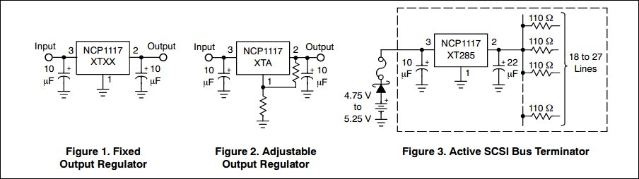
image taken from the voltage regulator datasheet
My final project also consists of a manual. As I have explained above the idea of the post-collapse networking device is that people who may not have a lot of knowledge of networking may build it in a time of crisis. Therefore a manual on how to build the device is important.
The manual is made with composites using jute and epoxy. It was made into a book with coptic stitching. I hope that the explananation given on this page above is enough. If more information is needed than week16 provides an exhaustive desctiption on how the book/manual was made.
The book also serves as a lid for the casing of the post-collapse networking device.
The final project also consists of a CNC’d casing with lasercutted dividers as its interior.