4. Electronics production
Amsterdam, February 19, 2020
To do:
Make a FabTinyISP.
Source files
| Description | link |
|---|---|
| Firmware for the FabTinyISP | Downloadable zip. |
| Traces file FabTinyISP | Downloadable PNG. |
| Cutout file FabTinyISP | Downloadable PNG. |
| Traces file FTDI | Downloadable PNG |
| Cutout file FTDI | Downloadable PNG |
| Photo image of FTDI | Downloadable JPG |
| Schematic of FTDI. Look under: host communication > FTDI > chip > hello etc | Downloadable JPG |
urls
| Description | link |
|---|---|
| Index of this week’s topic | http://academy.cba.mit.edu/classes/electronics_production/index.html |
| Global lecture video | https://vimeo.com/388201669 |
| Global review video | https://vimeo.com/394033124 |
| Documentation page FabTinyISP | http://fab.cba.mit.edu/classes/863.16/doc/projects/ftsmin/index.html |
| Group assignment documentation | https://fabacademy.org/2020/labs/waag/groupAssignments/week4.html |
| Documentation page FTDI | http://academy.cba.mit.edu/classes/embedded_programming/index.html |
Milling machine
General
We have a Roland Modela MDX-20 milling machine. A small milling machine that is pretty precise. We make PCBs with it. You could use it for making molds too. But we don’t do that because it is messy and the machine does not like that. We do molding on the Shopbot.
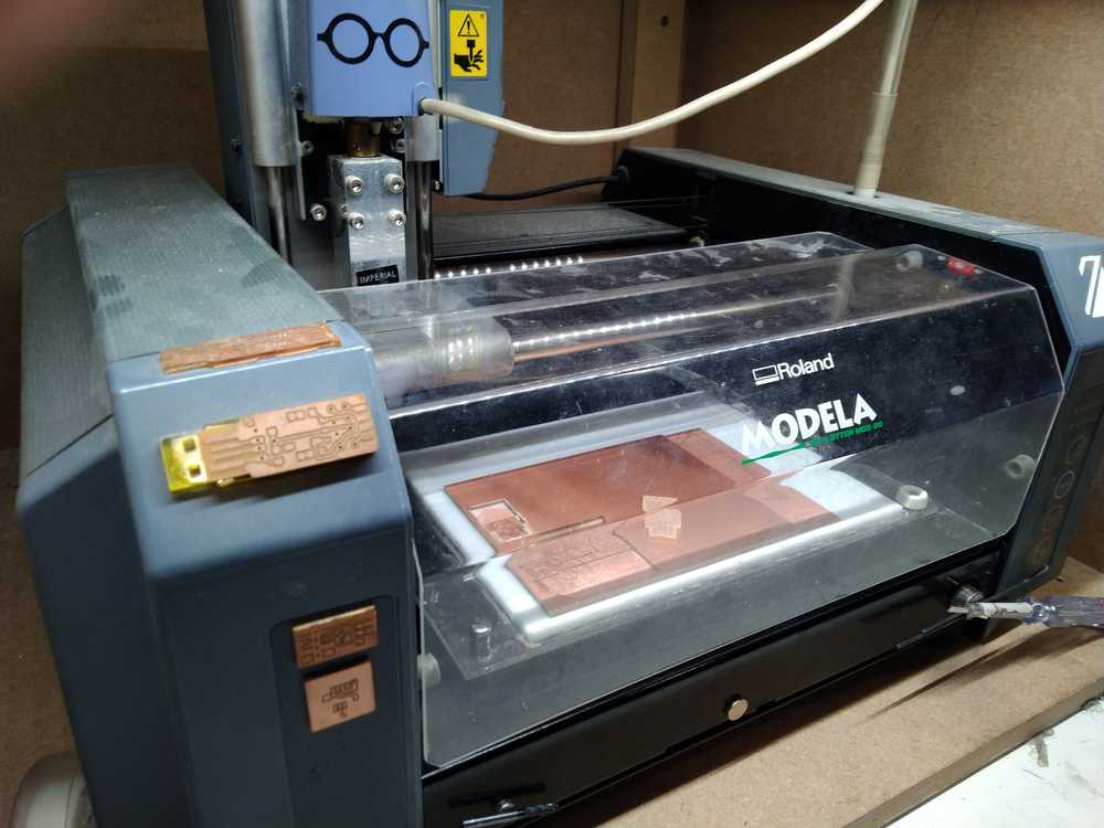 Roland MDX-20 milling machine.
Boards
We use boards with a thin copper layer on a substrate of pressed paper. They’re called FR1. FR4 is a glass fiber substrate. We use two types of milling bits. To make the traces we use a 0.4 mm drill. To do the cutout we use a 0.8 mm drill.
Bits
There are different kinds of drills. 0.4 mm is for tracing. 0.8 is for cutting out the board. 0.1 is a thinner bit for tracing but we don’t use them. Drills can have 1 flute or 2 flutes, or one knife or two knifes.
 0.4 and 0.8 bits.
 Drawing of a 1 flute (above) and a 2 flute drill (below).
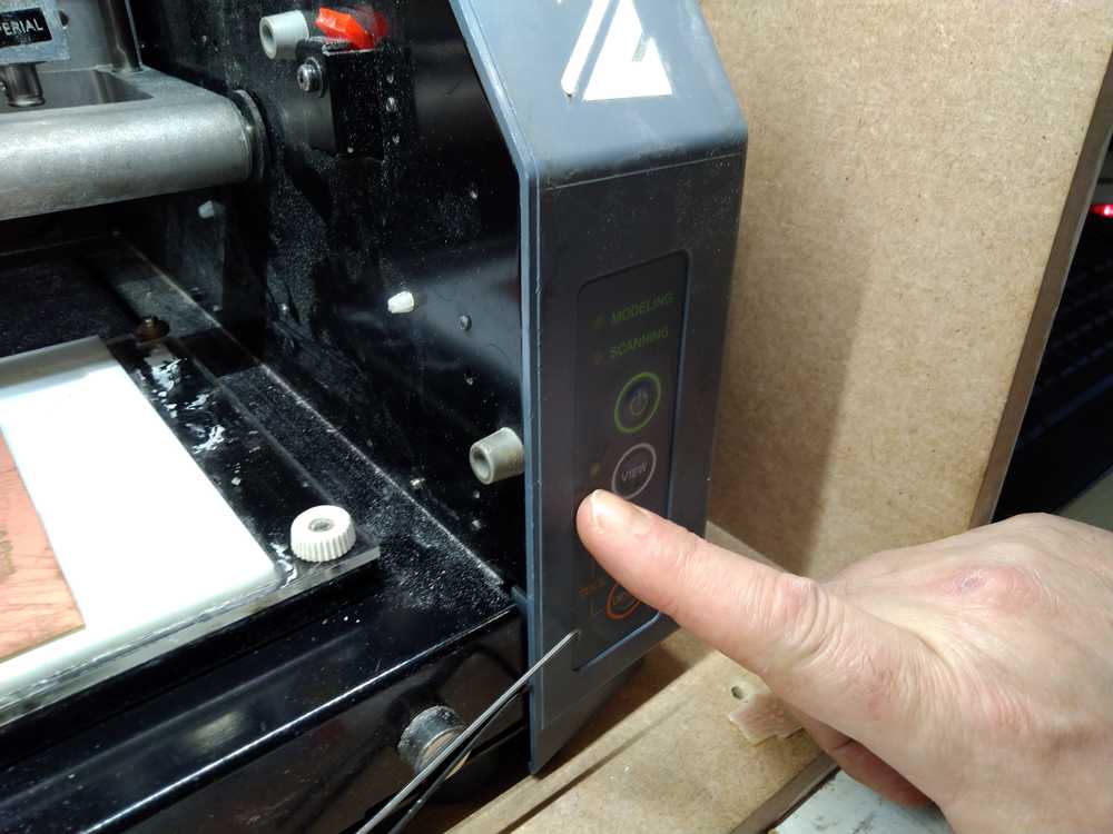
View button
Pressing it once will put it in View Mode: at the top-right with the machine bed all the way extended toward you. Pressing it again will move it to the origin of the board, the lower left point of the board.
Hardware
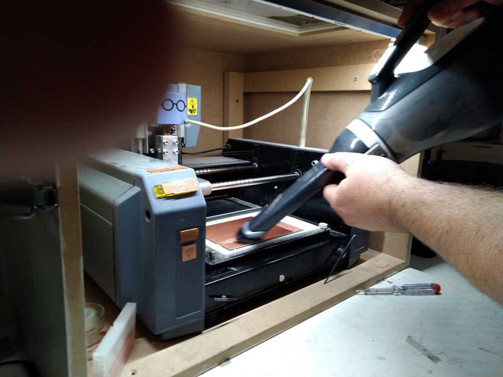
Press View on the control panel of the machine. The head will move to the top right corner. The bed will extend all the way toward you. You can now handle the bed.
 Unscrew the bed from the machine.
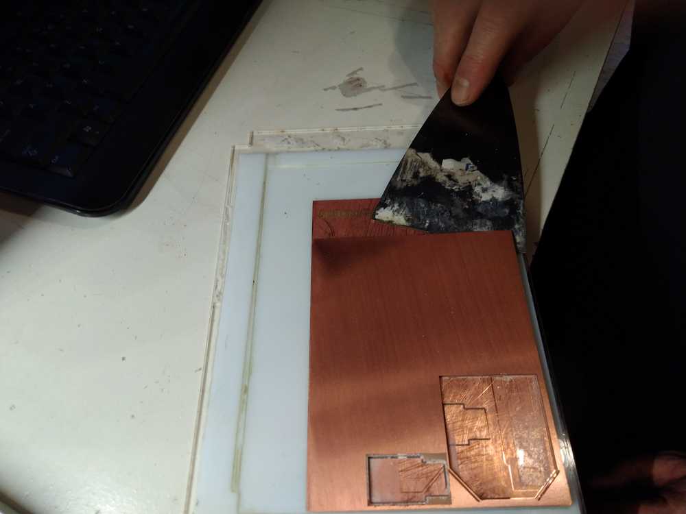 Use a scraper to unfasten the board from the sacrificial layer, if there is one on there from a previous run. (The sacraficial layer is an extra layer attached to the bed. It can be sacrificed if someone accidently cuts too deep.). Pressure is needed.
 The board is now free from the bed.
 The sacraficial layer needs to be very clean. It needs to be smooth so the board is completely straight on the bed. Remove large pieces of tape from the sacraficial layer manually.
 Use sticker remover and paper to remove the rest of the tape off the sacrificial.
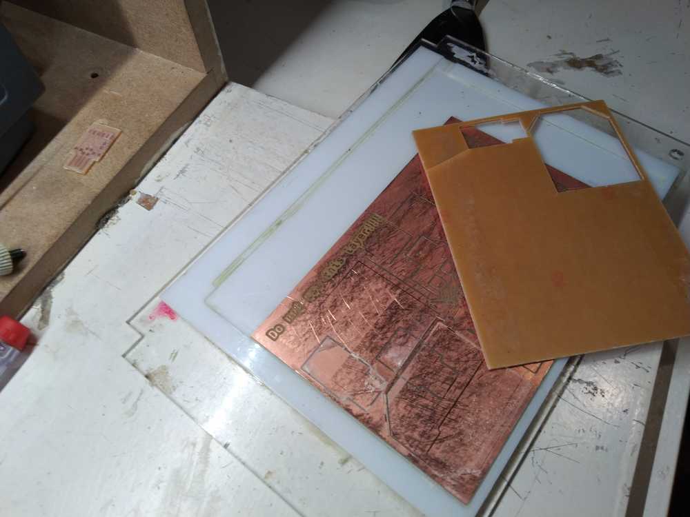
 The location of the boards.
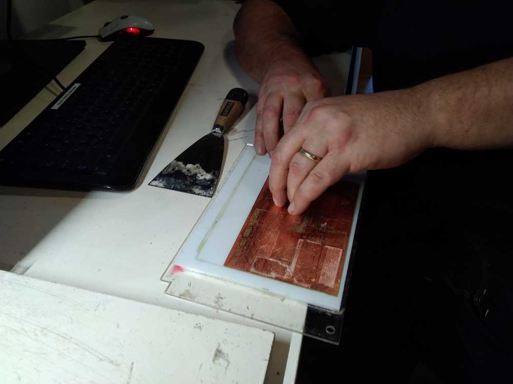
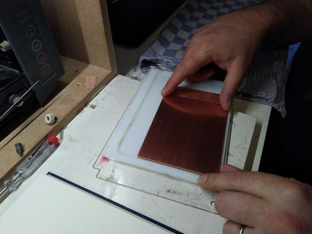
 Place the board with the copper layer downward on a cloth in order not to scratch the copper.
 Place double-sided tape on the back of the board. Use plenty. Basically place rows from the top all the way to the bottom with little space in between.
 Location of the tape.
 Stick the board on to the sacraficial layer on the bed. Make it straight. The machine does not care if it’s crooked or not, but for your own orientation straightness is preferable.
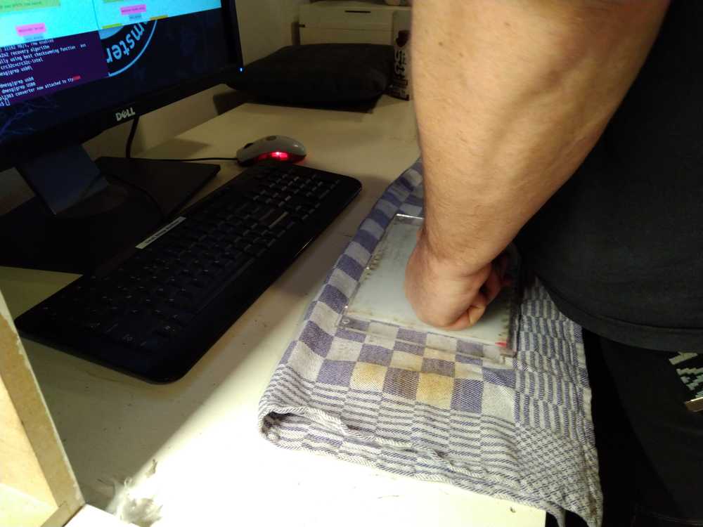 Press the bed down hard to make the board stick. Use the cloth again to protect the copper layer.
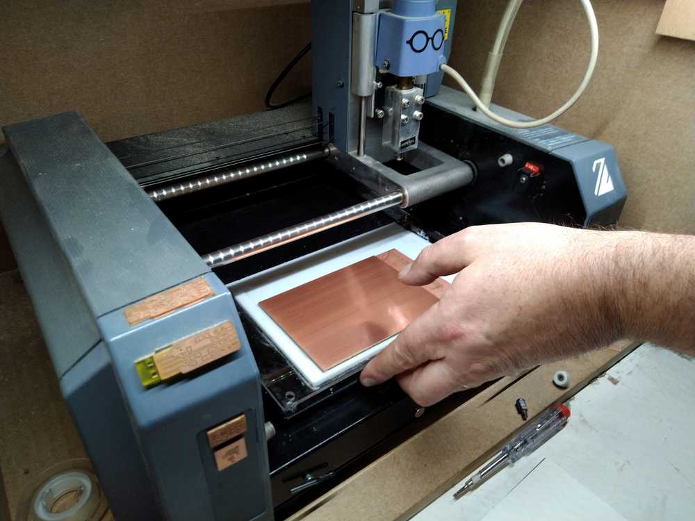 Place on the bed of the machine.
 Screw the bed tight, not too tight.
 Press view to take the bed out of view mode (bed extended forward). The bed will go to the back and the drill head will now go to the origin (lower left of the board).
 Drill head is at origin.
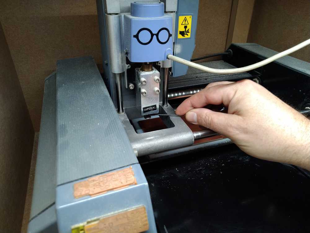 To insert a drill, screw open the hole where the drill is to fit in. Use an alan wrench. The hole to place the wrench in is at the bottom of the head near the drill.
 This is where the drills are kept.
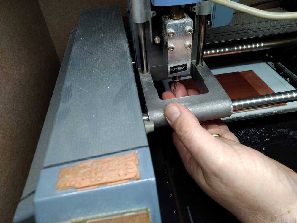 Place in a drill in the head. Hold the drill between two fingers with your palm facing upward. This will prevent the drill from falling down. If it does the tip might very well break.
 Tighten the drill fast with the alan wrench. First you put the drill almost as far in as it will go.
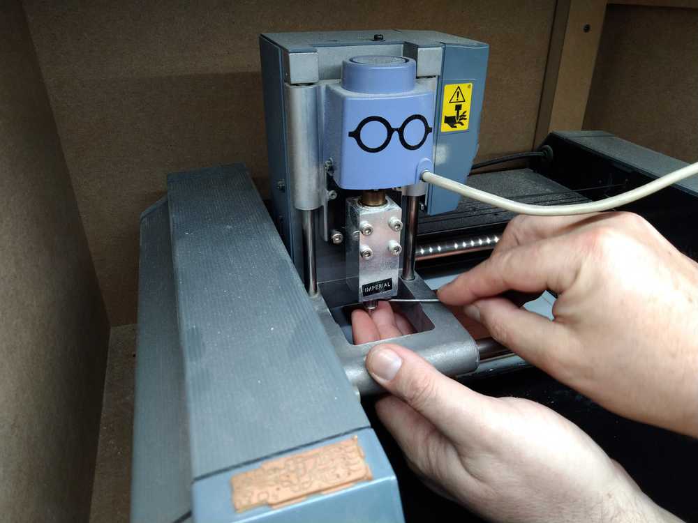
 In mods in the Roland module click move to origin.
Go first to software before doing the next two steps.
 The drill is now above your board. Use the down button to lower the head’s Z-axis.You bring the Z-axis of the drill all the way down. Then you lift it up again.
 The drill must have space to be able to go up and down. If your Z-axis is extended all the way down, the head has no room to lower. And thus it will be unable to cut the copper layer. For tracing you need less space for the Z-axis. For cutting you need more space because the drill has to go all the way through the board.
So: bring Z-axis all the way down. Move up a little. Now loosen the drill in the had and gently lower it manually until it touches the copper layer.
Then screw the dril tight again.
Software
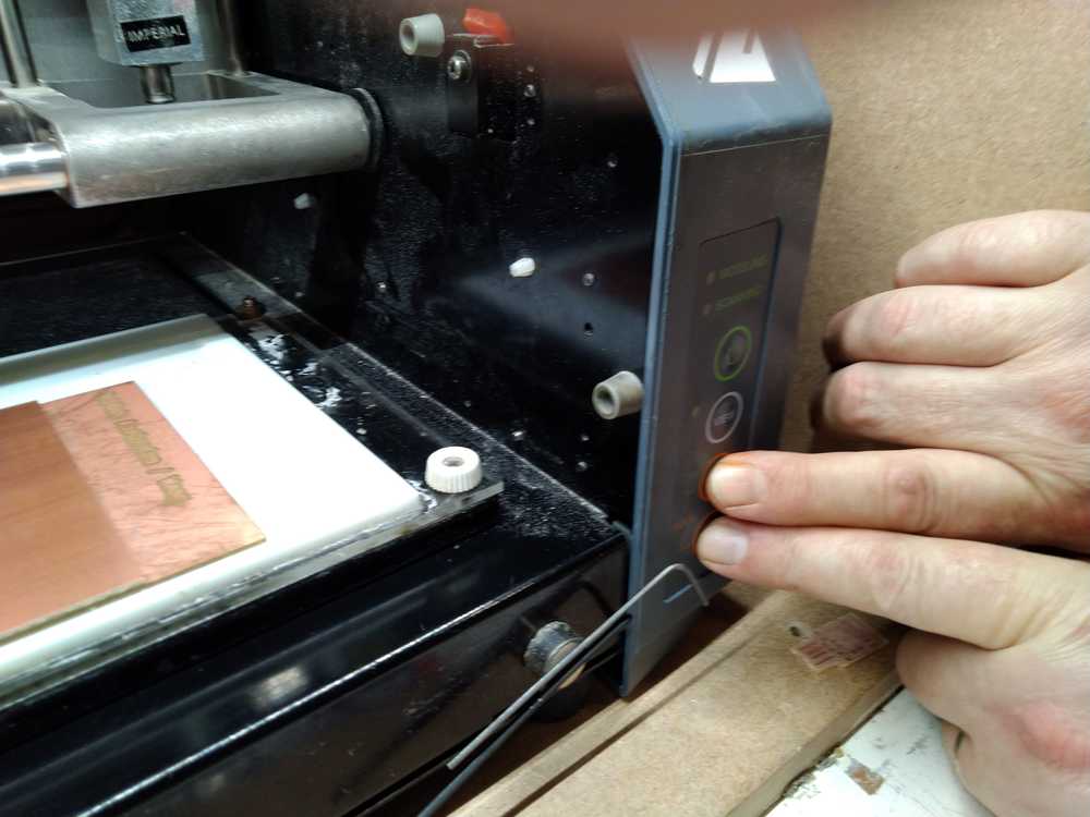
We use Mods software. Mods opens devices on different ports. The machines have networking addresses and they are listening on a port. If the computer sends a file to that port they will recieve it. The milling machine and the vinyl cutter work with Mods.
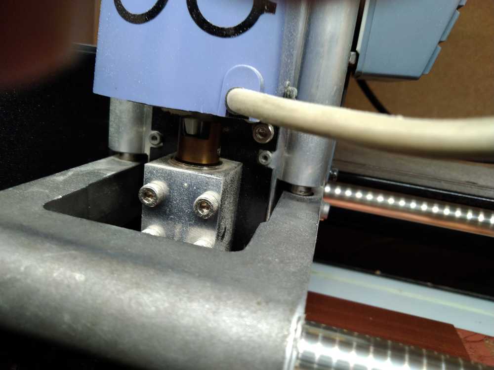
Turn the milling machine on in order for the software to find it on the network. Power on will cause the head to move to View mode. In View mode the head is top-right in the back. And the milling bed is extended all the way forward. (View refers to being able to view your board.)
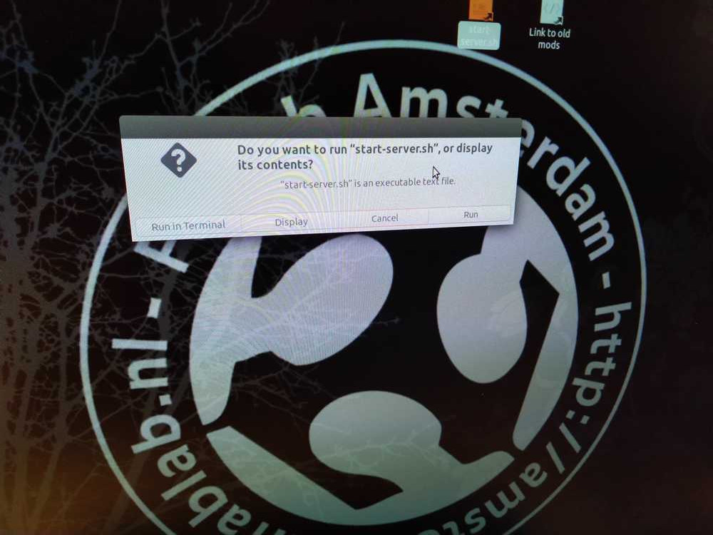
You start it up by clicking the icon on the desktop saying: start-server.ssh. The other icon is the link to the other version of Mods.
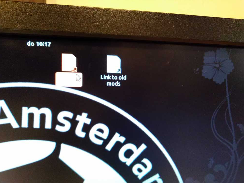 Selected is the new link to Mods
Run in terminal? Yes. This opens a terminal in Firefox.
 Run in terminal.
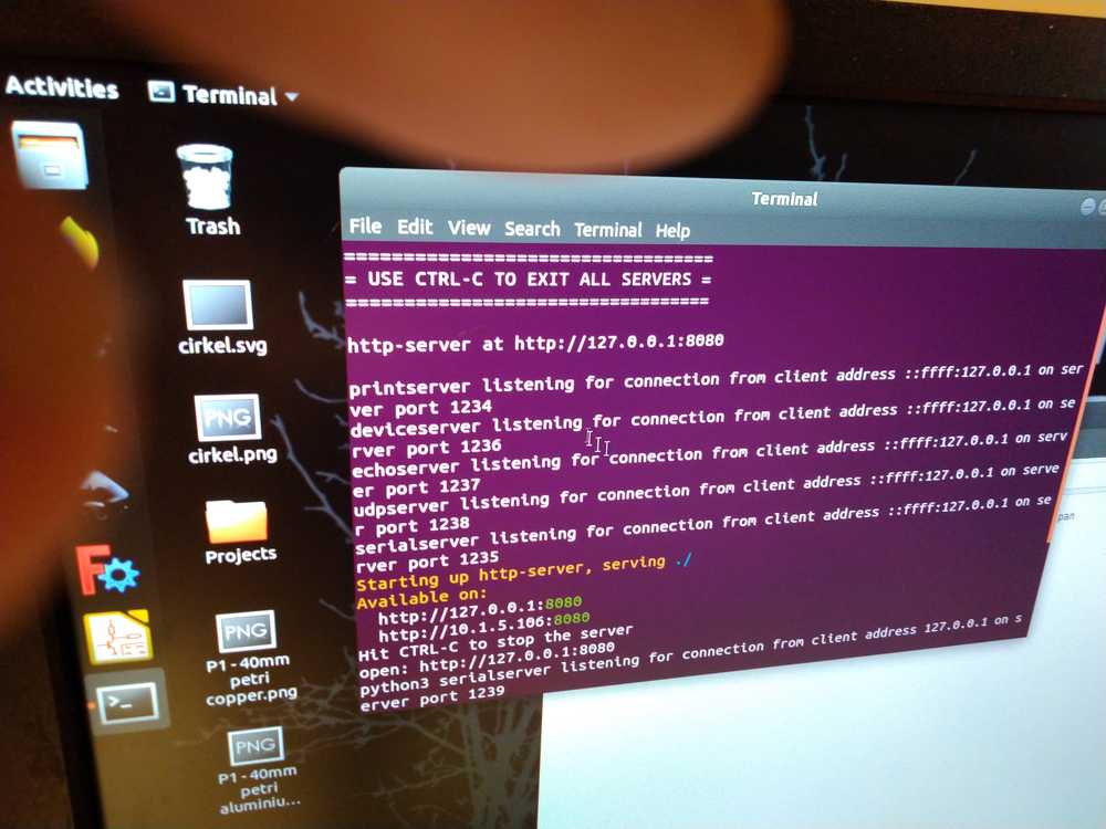 In the terminal you can see the different servers Mods is interacting with and the ports these servers are listening on.
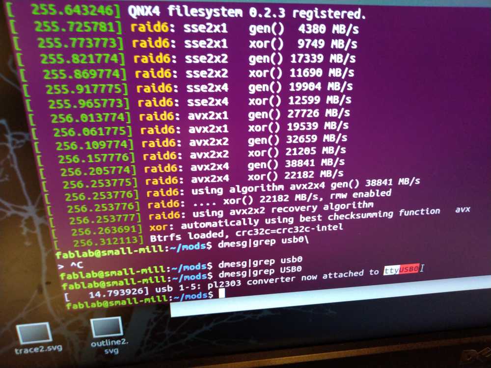 type dmesg|grep USB0 in the terminal. You can now see in the terminal that it is connected to device ttyUSB0.
 Right click to open menu.
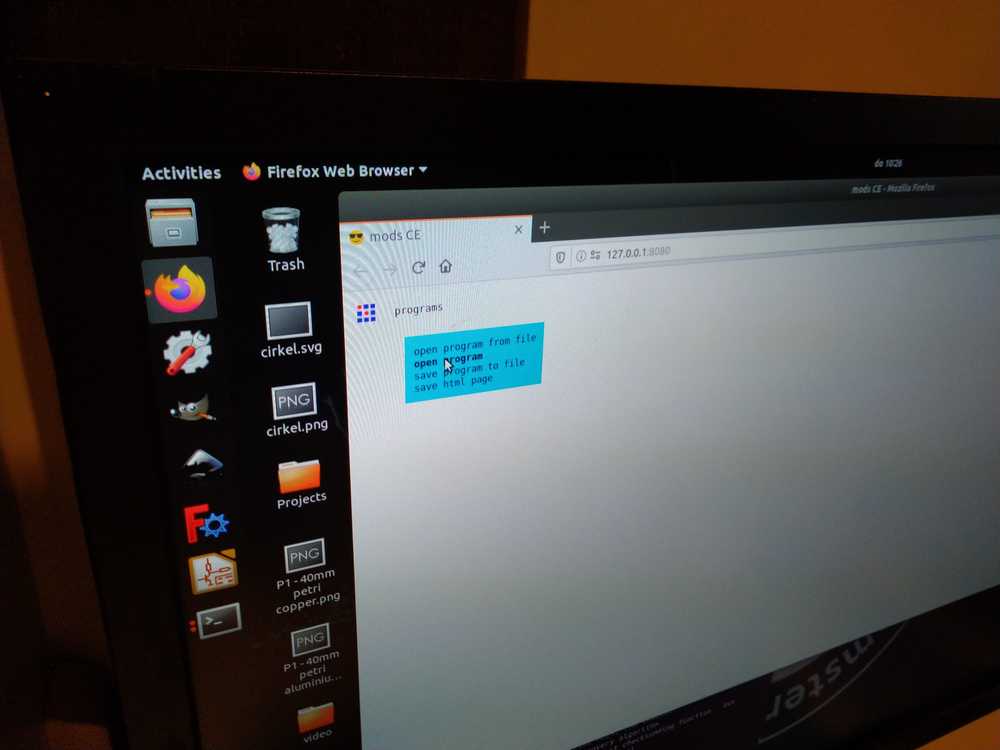 Open programs.
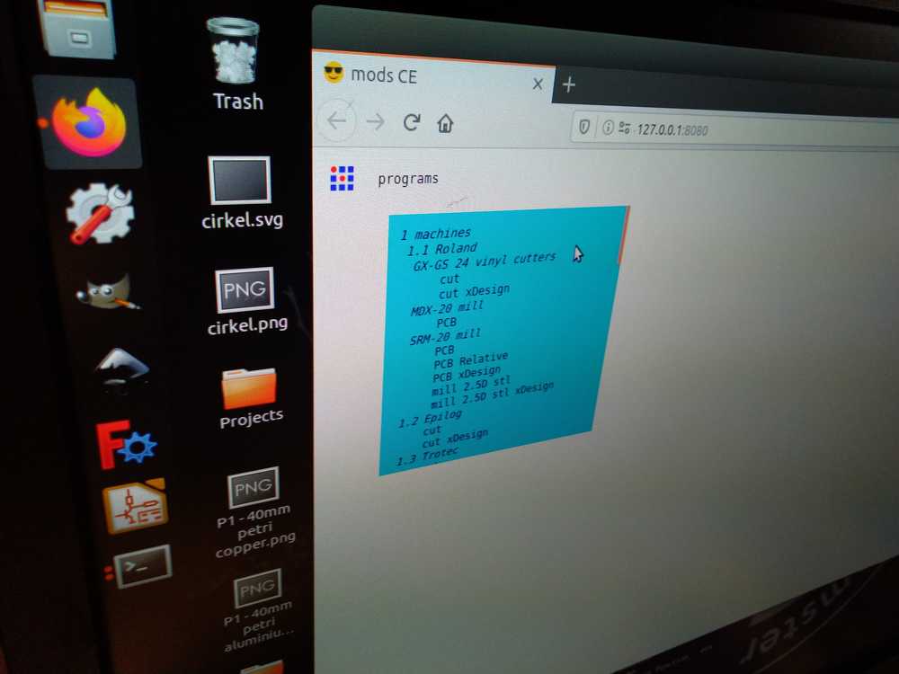 Choose MDX-20 Mill > PCB.
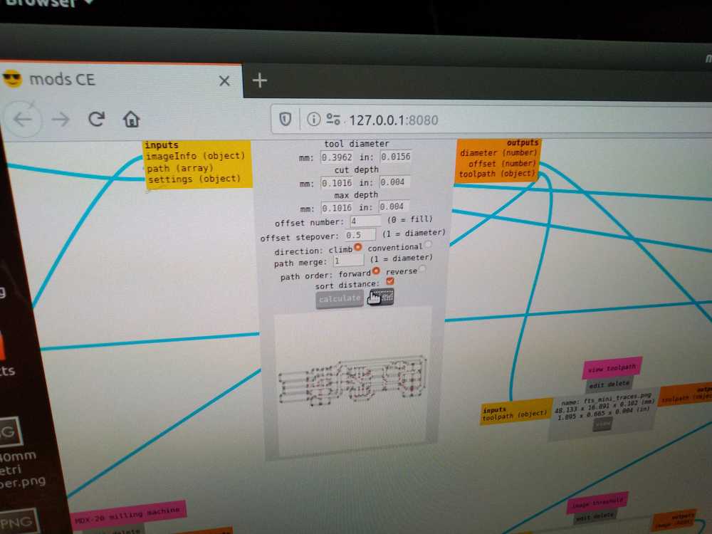
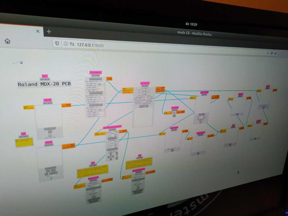 This is Mods. Mods stands for modules. Each rectangle on the screen is a module. Mods is a flow of modules that each generate G-code for the machine according to the settings you choose.
Note the connecting lines. You can see that a line from one module serves as the input for another module. You can see what it is import for.
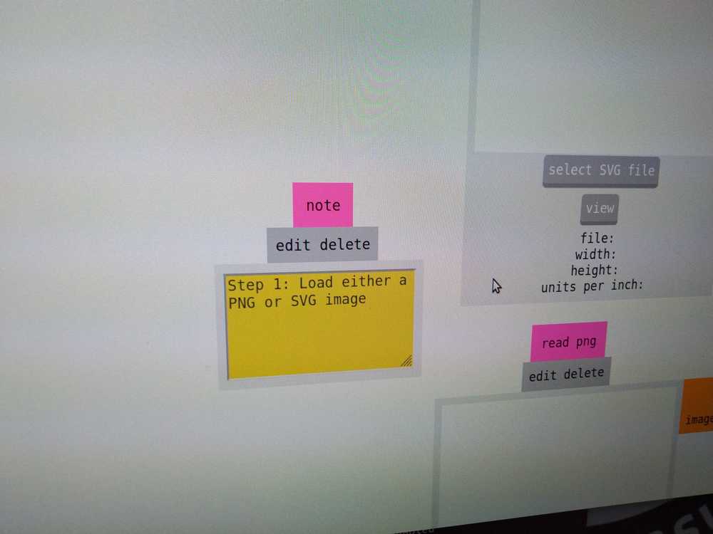 Modules: Read PNG or Read SVG. Use one of the modules to either import a PNG or an SVG. Don’t work from a USB stick. Copy your files first to the computers hard disc on path: Desktop/projects/fabacademy_2020/yourname/.
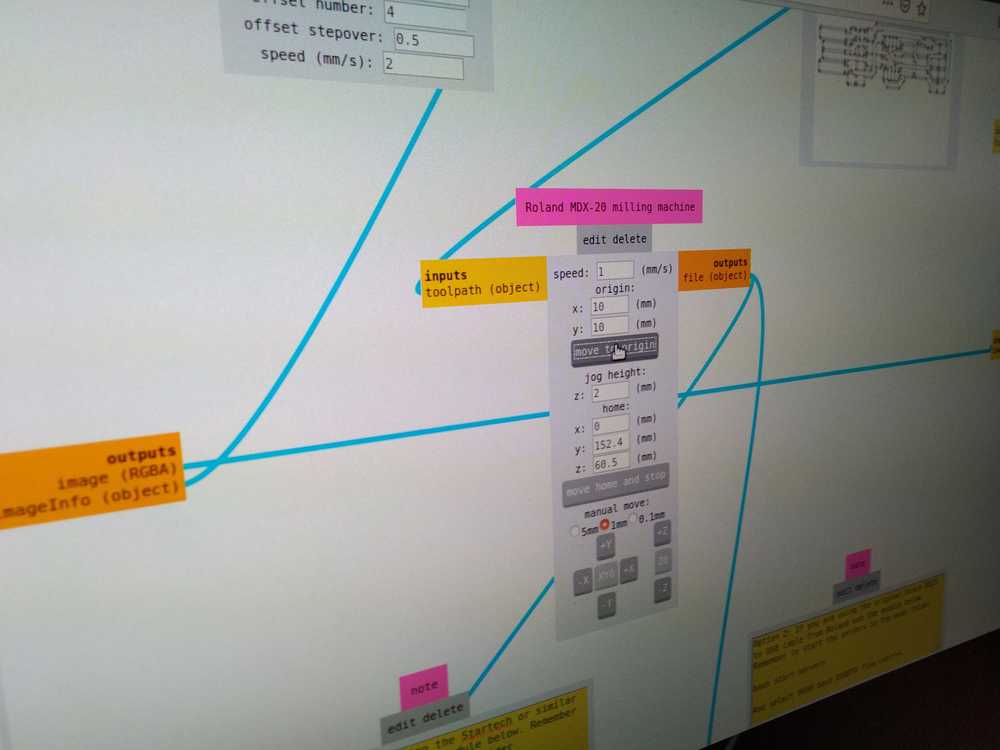
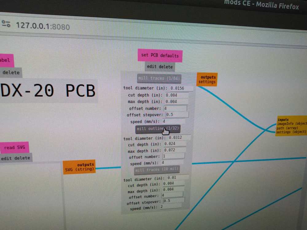 Module: set PCB default. Here you choose what you are going to do: Mill traces 1/64, Mill outline 1/32, Mill traces 10 mil (1 mil = 0.0254mm) . We use the upper Mill traces 1/64 for milling traces. The outline for making the cutting of the board. We do not use the 10 mil traces, that is so small that the drill bit will break to often. We leave the settings as they are, we only use this module to choose which operation we want to perform.
Note: If you press Mill traces again, settings in the Mill Raster will revert to deault.
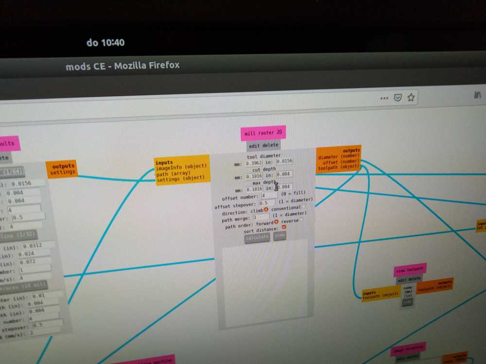 Module Mill raster: When you click one of the settings in set PCB, you see the numbers change in the Mill raster module. You can see the Mods line running from the output settings of the set PCB module to the settings of the Mill raster module.
Settings:
Tool diameter: in the picture we see 0.3962. This is default, we do not change it. We choose the setting milling 1/64 in the PCB default module. For this we use the 0,4 mm drill. We see this reflected in the setting. If we choose Outline in the PCB setting, the drill is 0.8 mm & this will be shown in the Mill raster module. (This is done automatically. Don’t change these settings.).
Cut depth: This is how deep the drill will cut. It shows a minimum and a maximum depth. The max depth ensure that you won’t accidently cut very deep and hit the bed of the milling machine. These settings too are default and you need not change them.
Offset number: number of lines we want to cut. 1 line is very thin, therefore you usually cut multiple lines for a single trace. Default is 4. Placing it to 0 will edge all copper of the board accept for the traces.
Offset stepover: The mill will retrace a part of the line it has already cut out to make sure no copper is left between two lines. Usually we put this on 0.5.
Direction: climb or conventional. Climb is most used. Climb cuts from high to low into the trace. Conventional starts in the ‘valley’ and cuts upwards. In our group assignment we saw climb gave the better result both for 1 flute and 2 flute drills. For our group assignment we made a board on four settings: we saw
Path merge: leave at 1.
Path direction: leave as is: forward.
Sort distance: leave ticked on.
Calculate: press calculate when you want Mods to calculate the model. When you enter new settings you must press calculate for them to take effect.
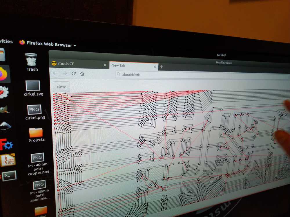
View: Press view to see an image of your circuit. It opens in new tab.*
 Press calculate to calculate the model. The image appears in the module. Press view to view it in a new tab.
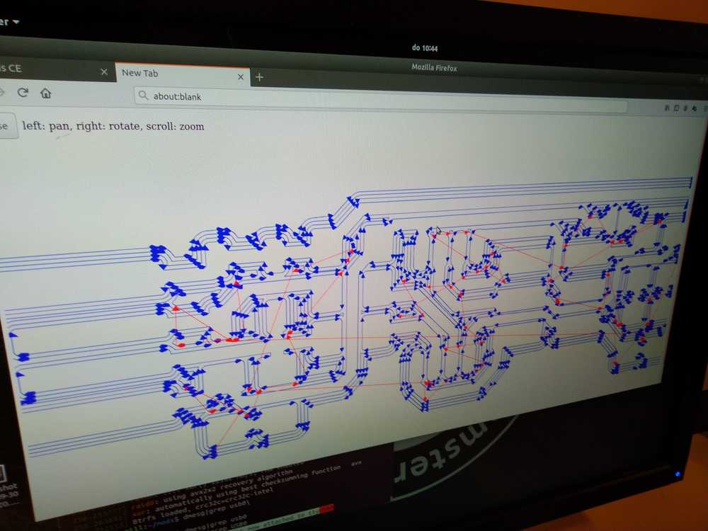 Image you see after pressing view. In this instance we have chosen offset number 4: the trace will consist of 4 lines.
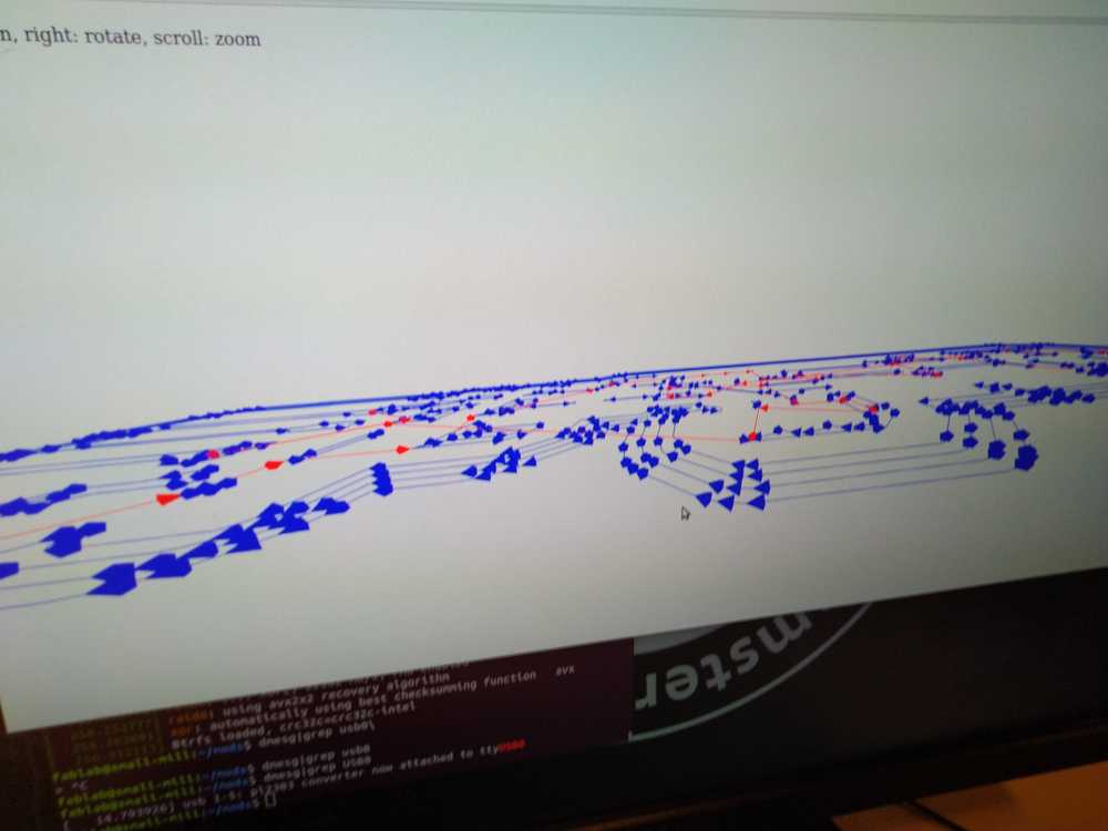 You can rotate the image over the z-axis. In this case you can see that the lines will be cut parallel to each other. When you do a cut out they will be below each other.
 Offset 1. One line. This will almost never be a good setting as the trace will be too thin.
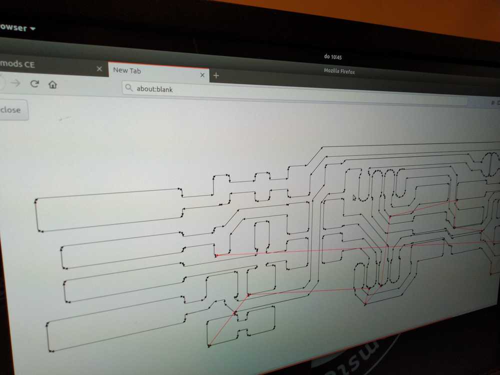
 Offset 0. The drill will clear the entire board of all the surplus copper.
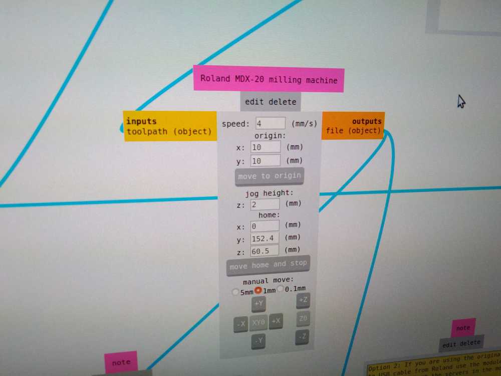 Module: Module Roland MX-D20.
Speed: for the 1/64 bit (the thin bit) we set this one to 1, to spare the bits. For the outline you can set it to 4.
View button Press the View button on the machine’s panel. The head will move out of View mode to Origin mode.
x-y-axes and origin. After having brought the head to the origin of the board, you can move the origin with the software. You can move the origin by changing the values to the x-y axes boxes. If nothing happens, check if your websocket ports are open.
Click Calculate.
Clicking ‘move to origin’ will bring the mill head there.
Write down you x-y axes. You need it again for the outline.
The drill is now above your board. Use the down button to lower the head’s Z-axis.You bring the Z-axis of the drill all the way down. Then you lift it up again.
The drill must have space to be able to go up and down. If your Z-axis is extended all the way down, the head has no room to lower. And thus it will be unable to cut the copper layer. For tracing you need less space for the Z-axis. For cutting you need more space because the drill has to go all the way through the board.
So: bring Z-axis all the way down. Move up a little. Now loosen the drill in the had and gently lower it manually until it touches the copper layer.
Then screw the dril tight again.
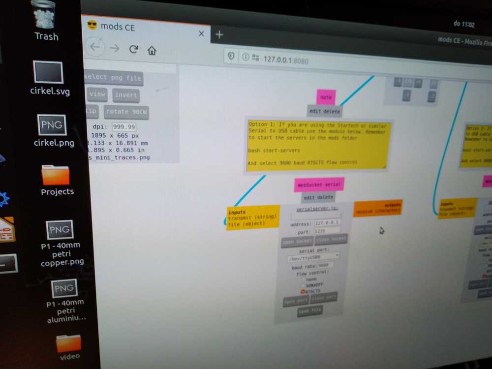 Module web socket:
We use the websocket module, not the Python module. (This has changed later. At the moment we use the Python module.) This is the module that is boss over the ports.
Check if the port and web socket are open.
Serial port says: /dev/ttyUSB0.
The settings are always on the same default: baud rate 9600 and
flow control RTSCTS ticked on. When you have to change the setting to RTSCTS make sure to press calculate and close and re-open ports for settings to take effect.
At the bottom of this module is the send file button that will send your file to the machine and it will start drilling. Don’t press send file yet. You need to prepare the machine first.
When you have prepared the machine you can run the job:
1. Note down you x and y axes settings to be used for the cut out process.
2. check that your z-axis is at the right hight.
3. check that the drill is lowered to the board.
4. Check that speed is in the right setting: 1 for traces, 4 for cutout.
5. check baud rate is 9600.
6. check flow control is RTSCTS.
7. Press calculate just to be sure.
8. close and open websocket and port. To have changes take effect.
9. Press send file in the web socket module.
Cut out.
Two different files are needed for tracing and cut-out. First you do tracing. Then the cut out.
- Change the drill to 0.8.
- For cut out you load a new file.
- Select Milling outline in the PCB socket.
- Choose offset 1 in the Mill raster Module.
- Calculate and view your model.
- Speed may now be changed to 4.
- In the Roland module place the origin at the exact same spot as you used for the tracing file.
- Give Z-axis drill head more space than during tracing.
- Lower the drill unto the board.
- Check flow control RTSCTS.
- Press calculate.
- Close and re-open ports and web sockets are open.
- Send file.
After cut is finished
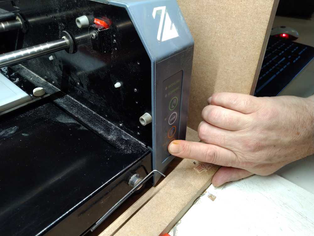
 Vaccuum the dust from the board.
Press View to bring bed forward.
 Use a screw driver to wriggle you cutout loose from the board.
Remove the surplus copper with a knife.
- Wash board with hand soap.
- Clean with water.
- Dry with paper.
- Rub with paper hard to make trace edges more smooth.
Trouble shooting
Stopping a job
Press View to stop milling.
Press View again: the head starts traveling back.
Then press up and down together for a few seconds as the head is traveling back to the origin. The View light will start blinking. Let go of up and down buttons.Meanwhile cancel the job in the software. Close the port and the websocket.
Wait for the head to be all the way to its final position. Wait till the View light has stopped blinking. This may take a while, maybe more than a minute.
Wait till head is all the way back and View light has stopped blinking.
Press View again, the head should move to the origin of the board and not start milling again. The machine is now reset.
To restart the job:
In the websocket module open the server and the port.
Press calculate.
Check x-y position by clicking and seeing where the head moves.
Press send file.
 Reset the machine by pressing View and then pressing up and down at the same time.
Short overview steps
- Press View on the control panel of the machine. The head will move to the top right corner. The bed will extend all the way toward you. You can now unscrew the bed.
- Place board top down on a cloth. Attach tape.
- Stick board to sacraficial layer.
- Lay upside down on a cloth and press hard.
- Screw bed back in machine.
- Press View. Head will move to origin of board.
- Check if the right drill is in the machine. Insert a drill pushing it in deep.
- Start mods: choose MDX-mill > PCB.
- Upload file.
- PCB default module: click Mill traces or Mill outline.
- Note: If you press Mill traces again further down in the process, settings in the Mill Raster will revert to deault.
- Check settings Module Mill raster: 0,4 for traces; 0.8 for cutout. Cut depth 0.1 for traces.
Offset number 4 is default for traces. Offset number 1 is default for outline/cutout.
Offset stepover: 0.5 is default.
Direction: climb is default.
Path merge: 1.
Path direction: forward.
Sort distance: leave ticked on. - Calculate.
- View.
- Module Roand MX-D20:
speed: tracing = 1 ; cutout = 4.
Press View button on the machine. Head will move to board’s origin. If this does not work, open the socket and port.
Adjust origin with X-Y in the MX-D20 module. - Click calculate.
- click move to origin.
- Write down X-Y settings in traces for use during cutout operation.
- On machine: lower Z-axis all the way down (drill must be fastened in deep).
- Move Z-axis up a little (it needs room to manouver).
- Unscrew the drill and gently lower drill to the copper layer.
- Websocket module:
check if port is open.
check baud rate 9600.
check flow control RTSCTS. If you have to change the flow control settings, close and open the ports for the new settings to take effect. - Final checks:
- Note down you x and y axes settings to be used for the cut out process.
- check that your z-axis is at the right hight.
- check that the drill is lowered to the board
- Check that speed is in the right setting: 1 for traces, 4 for cutout.
- check baud rate is 9600.
- check flow control is RTSCTS.
- Press calculate just to be sure.
- close and open websocket and port. To have changes take effect.
- Press send file in the web socket module.
Soldering
- Your board must be clean for soldering. So rub with hand soap, rinse with water, dry with paper. Don’t touch top layer with your fingers after cleaning because your fingers have fat oils on them.
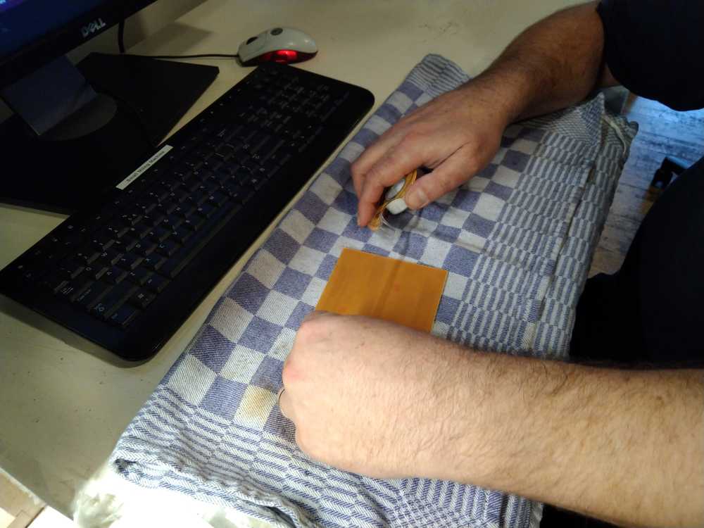
- You board will still have tape on the bottom from milling. Use it to stick your little board on a piece of paper. Now you have a larger surface to grab a hold off.
We’re doing SMD soldering this week: Surface Mount soldering.
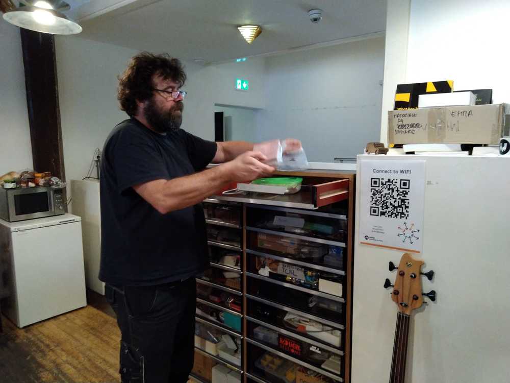
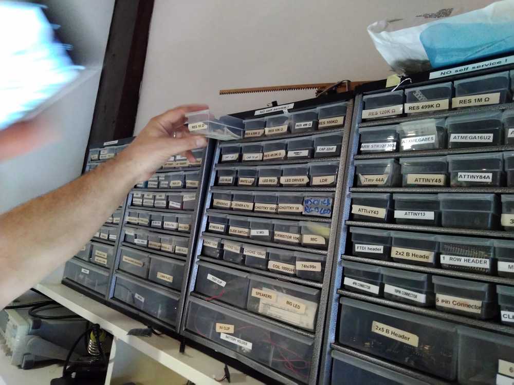 Check the designs files to see what components you need. The components are stored here. Take one component box, solder. Place component box back before you take a new component box. Otherwise you will loose overview and not know which component is which or where each box goes when putting them back.
Check in the design files if components have an orientation. If they do they have tiny markings. If you can’t see the marking use a magnifying glass.
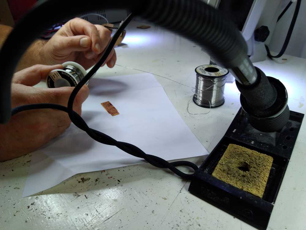 For small components we use thin solder wire.
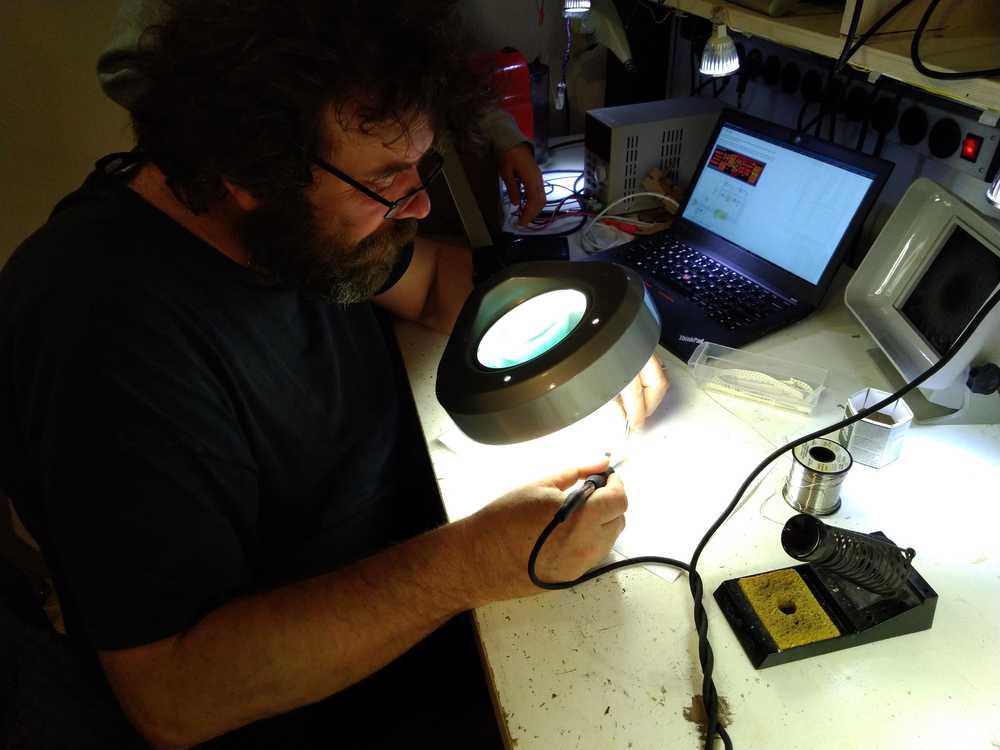 Use a magnifyer glass for a better view.
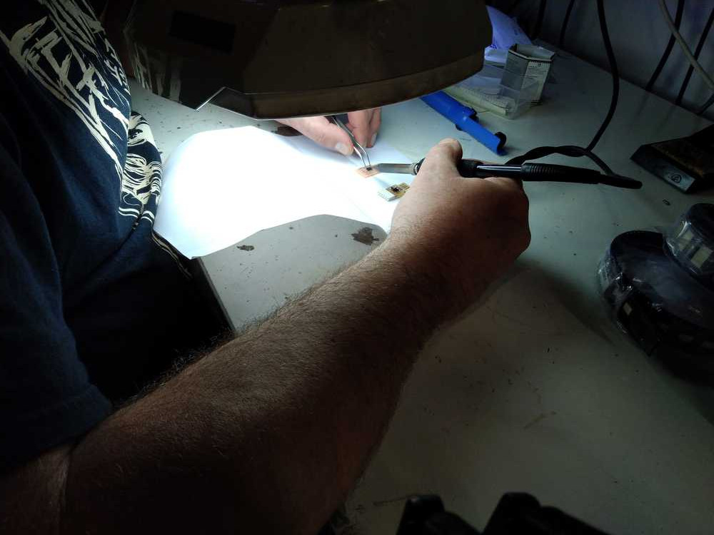
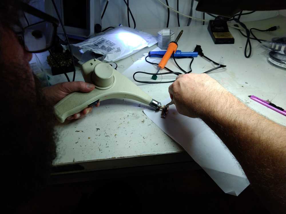
Soldering in action
preparing the solder pin:
1. Let it heat up.
2. Clean tip on wet sponge.
3. Add solder.
4. Clean tip again. Now you have a nice clean tip with a film of solder on it.
Four step soldering
1. Heat both trace and component leg.
2. Apply solder.
3. Retrieve solder wire.
4. Keep pen down. For a couple of seconds to keep the solder flowing. Retrieve pen.
To solder a small component.
1. Heat an island.
2. Apply a little blob of solder.
3. Get component between your tweezers.
4. Put 1 leg on top of blob.
5. Heat solder with pen.
6. Push leg in place.
7. Manouver the component in the right place. Are all legs nicely fitted on a trace?
Note: even if components have no orientation, you can place the lettering in the same direction for easy reading.
To solder a tiny component
Attach 1 leg of each side of the IC to the board using the method of applying solder first. Then apply solder over all the legs. Use the fancy desolder that heats up and use the sucking mechanism to remove the solder between the legs of the IC. Look carefully through a magnifying glass if all surplus solder is removed. If necessary use a knife to remove the surplus solder.
 Solder 2 legs of the IC on their islands first. Then spread solder over all the legs.
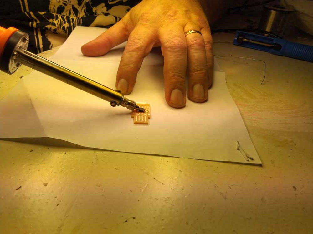 Use the fancy solder sucker that produces its own heated air. It’ll melt the solder and you can suck it out from between the IC’s legs.
Desoldering an IC
Use a heat gun. It outputs a stream of heated air on the board. Pick up the board by the component and hold it in the air. Use a tweezer. When the solder melts, the board will fall down.
 The heat gun hangs left from the soldering station. There is a box in the components cabinet that holds it nozzle. After use let the nozzle cool down before removing it and placing it back in the box for heat gun components.
Group assignment
Here is the link to the group assignment documentation.
The goal of the group assignment was to test two types of bits and two types of milling: climb and conventional.
The bits are different because the have a different number of flutes. The flute is the knife. We used a bit with 1 flute and one with 2 flutes.
We tested to types of milling: climb and conventional.
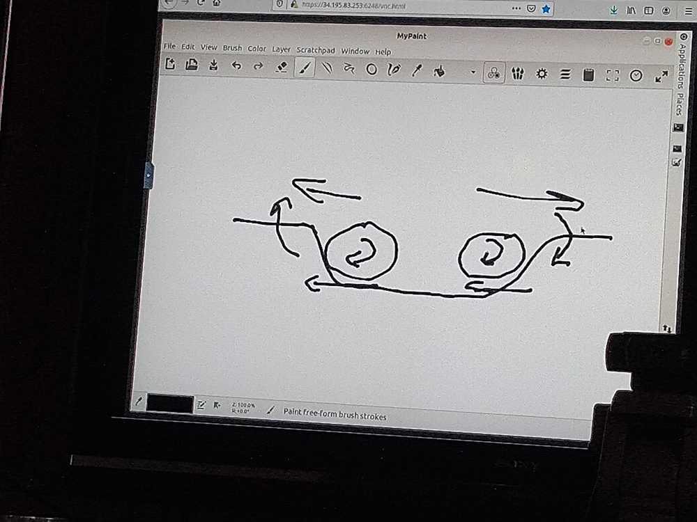 Schematic of climb milling versus conventional milling by Neil from the global lecture.*
Climb is the most often used setting. In this picture Neil shows the difference. With climb (right in the picture) the knife cuts the ‘mountain side’ of the trace into the valley. With conventional milling the knife moves from inside the ‘valley’ of the trace and cuts the ‘mountain side’ (left in picture.).
Our conclusion was that for thin lines the best setting is a bit with one flute using climb milling.
What I’ve learned from this assignment is using the milling machine. First Henk showed us how to use it. Then we worked on the milling machine together making this assignment. It took quite a long time to accomplish it. There are many steps in the process and you can do quite a few things wrong. The biggest hickup was when we did the wrong settings and we had to reset the machine. That means: making it stop wanting to do the file that was send and start with a new slate. We have done the troubleshooting manouver (see descripotion above) so often that by now I think I know it.
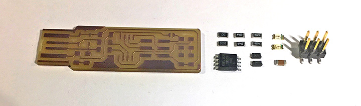
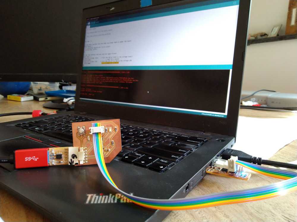
Individual assignment 1: making the FabTinyUSB
Milling
Each of us are making a FabTinyISP for this week. How to make this board is really well documented at this page.
I download both the traces file and the outline file.
From there on I tried to repreoduce the steps we had learned before from Henk’s explanation and the group assignment. I still made multiple mistakes. I had documented the steps Henk showed us. During this individual assignment I corrected the mistakes I had made in my documentation.
The things that went wrong:
1. I opened the Roland vinyl cutter instead of the Roland milling machine. I noticed because the module PCB defaults was missing.
2. Twice I stopped the mill. It moved from the origin point without drilling. I thought something had gone wrong. It turned out that the drilling did not start from the origin point. The head was simply moving to the first place it would set the drill in. So first movement without drilling does not mean it went wrong.
3. Twice the mill did really weird movements. This was because my flow control was in the wrong setting. I added to the final steps to check if your flow control setting is at RTSCTS.
Settings:
The x-y axes I used were: x 70, y 35.
After having milled the board I started with reading the entire how-to page for the FabTinyISP linked to above. The documentation warns that using USB 3 can cause problems. I checked the specs of my T460 Thinkpad, all three USB ports are generation 3. Something to keep in mind. Maybe use an older computer. (This turned out not to be a problem.)
Soldering
I removed the piece of copper at the front of the board near the USB connectors. Because this may short the USB port on your computer. Washed the board with handsoap. Dried with paper.
Heated the solder pen. When the light of the solder station flickers it is heating up. Light on permanently means it’s reached max heat.
Prepared the pen by heating it up, cleaning on wet sponge, adding solder, cleaning on wet sponge again.
Started with soldering on the ATtiny IC. Looked at the marking and placed in right orientation. First added blob of solder on the board using the heat first, apply solder, retrieve solder, retrieve pen method.
Mistakes:
Adding the LEDs I forgot to switch LEDs and now have 2 blue LEDs instead of different colors.
Note: The left LED is the power indicator, the right LED lights when the programmer is talking to the target.
At first I was worried when solder would stream away from the islands and start running over the traces. But this is okay, they’re both conductive materials.
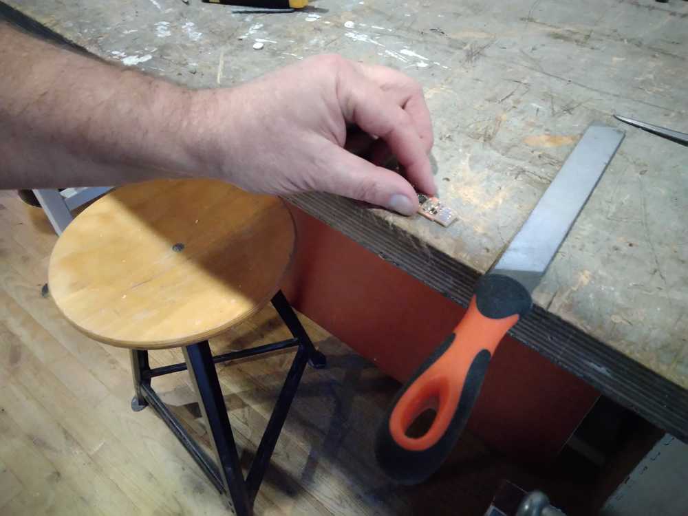
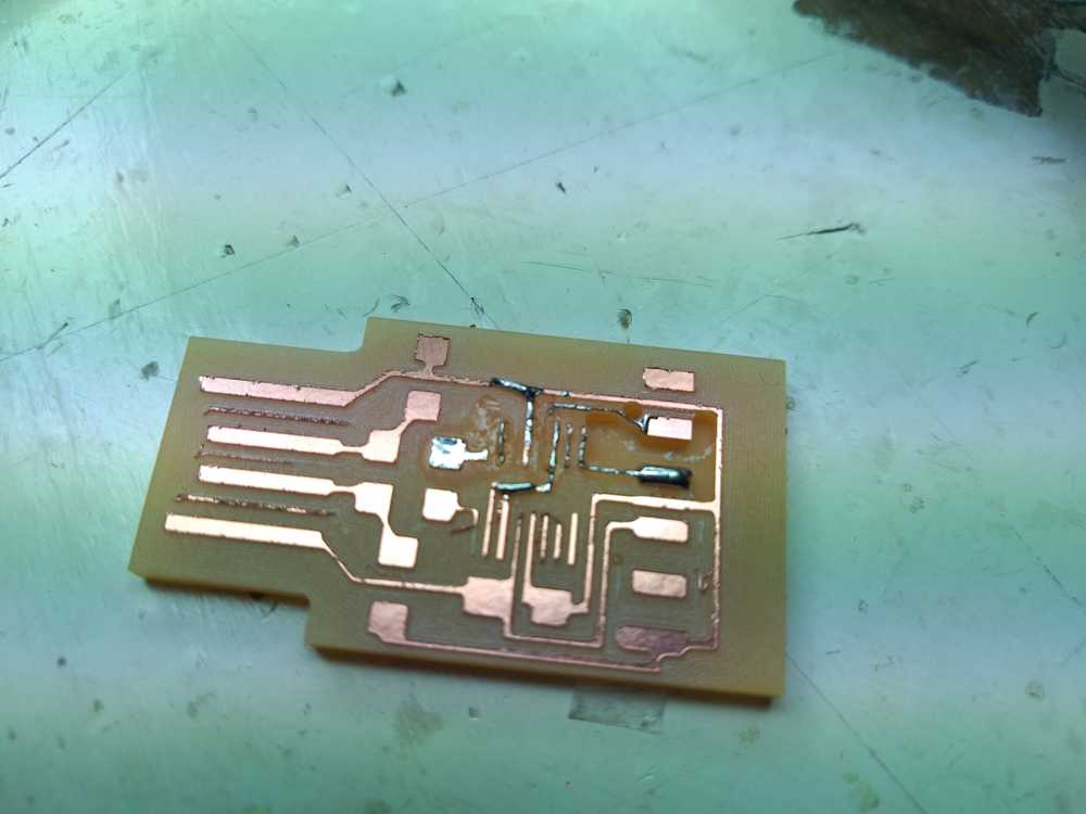
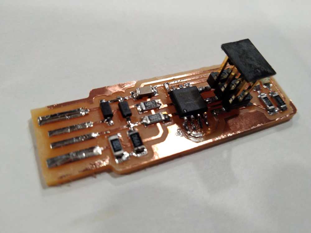 The finished board.
Programming
Back to the documentation. It advises to check your work. The ‘how to survive FabAcademy’ video advised to make a debugging table.
I noticed that the Zener diodes aren’t nicely aligned. I checked against the schematic and it seems this should be okay. But I’ll make a note of it.
Debugging table
| action | done |
|---|---|
| Hardware | |
| Copper lines same as schematic | checked |
| layout of components | checked but mind the Zener diode. |
| Test circuits with multimeter | checked |
| Check out right orientation of components | checked |
| Check out do you have the right components | checked |
| periferal devices | |
| Try different USB port | checked |
| Test on another computer that has been successfull with other ISP | checked |
| Software | |
| Check if you can flash firmware again | checked |
| research | |
| Run error messages through internet | done |
I install AVRdude with the command: sudo apt install avrdude gcc-avr avr-libc make. AVRdude ‘is a utility to download/upload/manipulate the ROM and EEPROM contents of AVR microcontrollers using the in-system programming technique (ISP)’ source: nongnu.org. In my own words: we used AVR to communicate with the ISP before it was programmed. On the documentation page they refer to AVRdude as a development environment. So AVRdude is a development environment. It can communicate to both the programmer and the FabTinyISP. It uses the programmer to program the FabTinyISP.
I download the firmware from the documentation page for the tinyISP and unzip with Ubuntu’s archive manager. (See also in my source files.)
Henk came to check if my ISP works on my computer. I have only USB 3 ports and some of my class mates had problems with that. Henk did:
dmesg (dmesg (diagnostic message) is a command on most Unix-like operating systems that prints the message buffer of the kernel. The output of this command typically contains the messages produced by the device drivers. Source: wikipedia). In my own words: it seems to print out all the internal chatter of the computer that pertains to devices and services that are running.
The terminal printed very much output but this is the important bit:
[ 8425.984613] thinkpad_acpi: EC reports that Thermal Table has changed
[11039.175780] usb 1-2: new low-speed USB device number 5 using xhci_hcd
[11039.365916] usb 1-2: New USB device found, idVendor=1781, idProduct=0c9f
[11039.365933] usb 1-2: New USB device strings: Mfr=0, Product=2, SerialNumber=0
[11039.365944] usb 1-2: Product: USBtinySPI
[11039.366633] usb 1-2: ep 0x81 - rounding interval to 64 microframes, ep desc says 80 microframes
My computer is seeing the TinyISP and calls it a low-speed USB device.
Then Henk typed: avrdude. This outputted the different command options for the program.
avrdude -c usbtiny -t t45 gave a long list of parts.
avrdude -c usbtiny -p t44 (so a ‘p’ flag instead of ‘t’) executed the right part:
avrdude: AVR device initialized and ready to accept instructions

Reading | ################################################## | 100% 0.00s

avrdude: Device signature = 0x1e9206 (probably t45)
avrdude: Expected signature for ATtiny44 is 1E 92 07
         Double check chip, or use -F to override this check.

avrdude done.  Thank you.
What this command does is that AVRdude is checking if it can see the AVR device (the FabTinyISP). The output shows AVRdude is seeing the AVR device and it can be programmed. The command does not execute anything, it is a way to check if AVRdude sees your devices.
dmesg again which resulted in:
[ 8425.984613] thinkpad_acpi: EC reports that Thermal Table has changed
[11039.175780] usb 1-2: new low-speed USB device number 5 using xhci_hcd
[11039.365916] usb 1-2: New USB device found, idVendor=1781, idProduct=0c9f
[11039.365933] usb 1-2: New USB device strings: Mfr=0, Product=2, SerialNumber=0
[11039.365944] usb 1-2: Product: USBtinySPI
[11039.366633] usb 1-2: ep 0x81 - rounding interval to 64 microframes, ep desc says 80 microframes
My computer still sees the tinyISP.
I then continue to build my firmware.
Standing in the directory of the firmware I type make
txl@T460:~/Documents/FabAcademy/classes/class04/board/firmware/fts_firmware_bdm_v1$ make
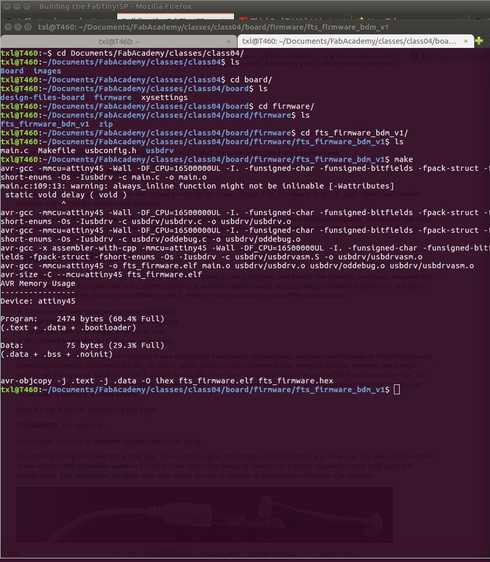
This command makes a new file with an .hex file extension. A hex file ‘is a hexadecimal source file typically used by programmable logic devices, such as microcontrollers. It contains settings, configuration information, or other data saved in a hexadecimal format. HEX files may be stored in either a binary or text format.’ Source: fileinfo.com.
This .hex file contains the code that will be programmed on the TinyISP. I now have a a file called fts_firmware.hex in the firmwarew directory.
I wondered why we have to make the hex file and why it wasn’t just part of the downloadable package. Henk explained the zip file contains the source files, these are human readable. You can make changes in these file. The Make command compiles the source files into machine code.
I open the makefile in the firmware dir with Nano. I make sure the right Programmer is named in the file. By default it says usbtiny and that is indeed the one we use. So I leave it as is.
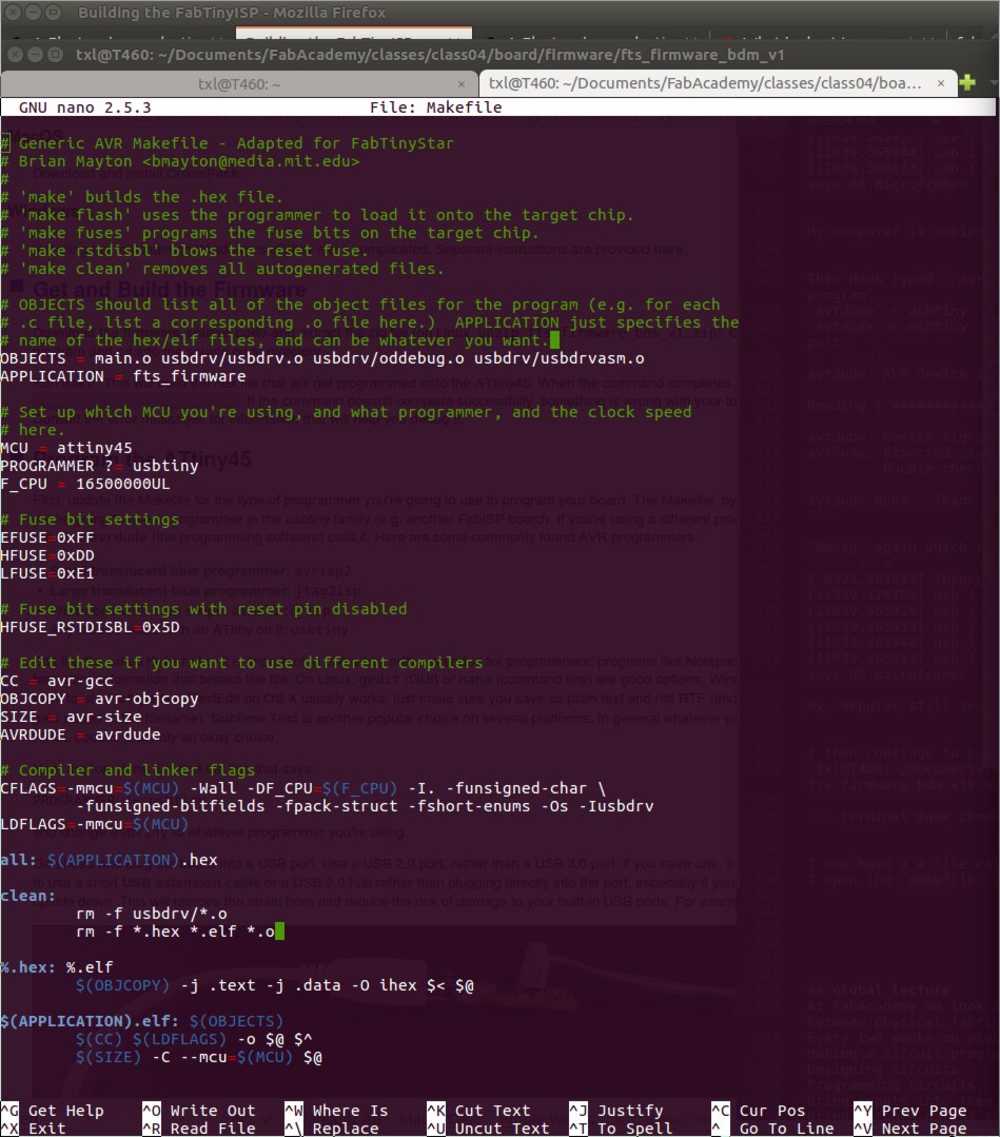 Make file
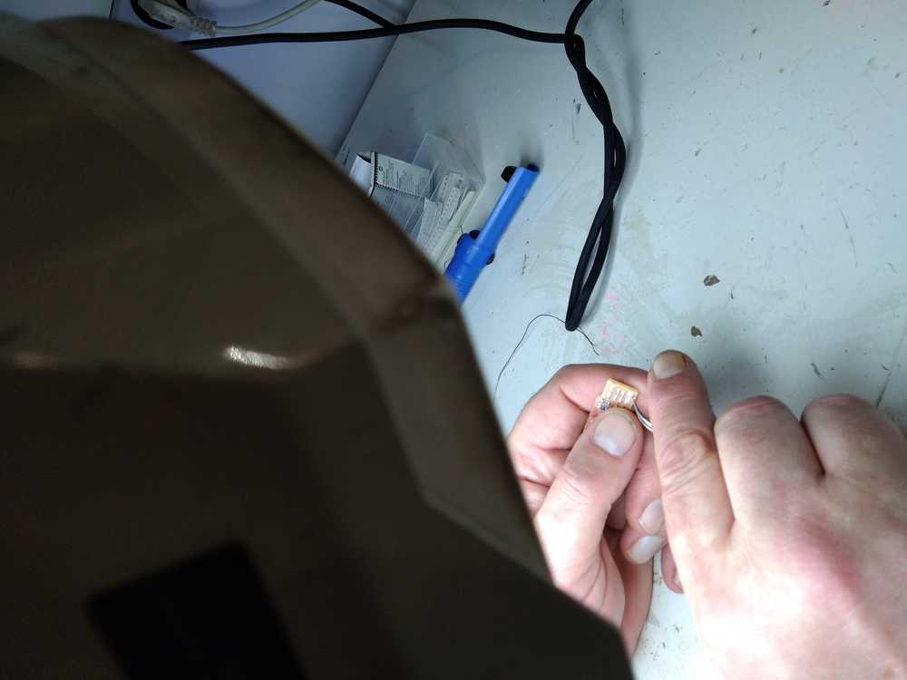
The board is plugged into my computer via a USB extension cable. The LED lights up. First test is a succes.
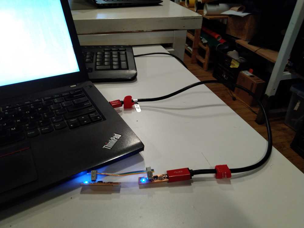 This image shows my programmer plugged into the computer and connected to the programmer that is going to be used to program my programmer.
When adding the programmer to the ISP note the orientation of the programmer. The pin connector must be rightly aligned to pin 1. Pin 1 of the 2x3 pin header on my board is the one vertical to GND. It is marked with a dot in the schematic. The connector that connects to the pins has a marking that denotes its pin 1. In our case it is a tiny triangle pointing to one of the pin connectors. Make sure that you connect the connectors of both the TinyISP and the programmer in the right way.
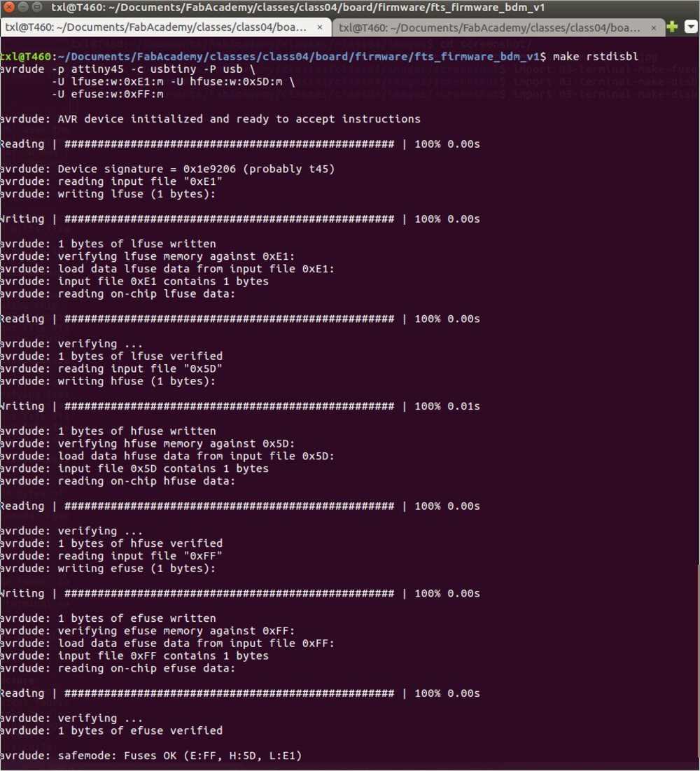
I run make flash from the firmware directory. It’s function is decribed in the makefile:
# 'make' builds the .hex file
# 'make flash' uses the programmer to load it onto the target chip.
# 'make fuses' programs the fuse bits on the target chip.
# make rsdisbl' blows the reset fuse.
# 'make clean' removes all autogenerated files.
make flash output:
avrdude -p attiny45 -c usbtiny -P usb -e \
    -U flash:w:fts_firmware.hex

avrdude: AVR device initialized and ready to accept instructions

Reading | ################################################## | 100% 0.00s

avrdude: Device signature = 0x1e9206 (probably t45)
avrdude: erasing chip
avrdude: reading input file "fts_firmware.hex"
avrdude: input file fts_firmware.hex auto detected as Intel Hex
avrdude: writing flash (2474 bytes):

Writing | ################################################## | 100% 3.75s

avrdude: 2474 bytes of flash written
avrdude: verifying flash memory against fts_firmware.hex:
avrdude: load data flash data from input file fts_firmware.hex:
avrdude: input file fts_firmware.hex auto detected as Intel Hex
avrdude: input file fts_firmware.hex contains 2474 bytes
avrdude: reading on-chip flash data:

Reading | ################################################## | 100% 5.64s

avrdude: verifying ...
avrdude: 2474 bytes of flash verified

avrdude: safemode: Fuses OK (E:FF, H:DF, L:62)

avrdude done.  Thank you.
So the make flash command goes to the programmer telling it to flash the chip with new firmware. In the output you can see that AVRdude is involved as well. It first erases the chip, removing any code that is on there. Than it flashes the code from the .hex file onto the chip.
Running make fuses command. ‘Every AVR microcontroller stores its configuration in a series of fuse bits.’ Source: hackaday.com‘ In our case it will configure where the microcontroller gets its clock source from. Source: documentation page.
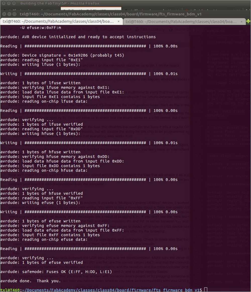
Now I test the TinyISP. I remove the programmer and plug the Tiny in on its own. i run lsusb. The computer recognizes the USB device as a tiny. Having done this I will now blow the reset pin. This means that the controller can never be reprogrammed again. Instead of a reset pin we’ll have a GPIO pin: a general-purpose input/output pin.
Running make rstdisbl
Now the board should work but it doesn’t. My computer does not recognize the device. It sees something is there but it can’t mount. I run dmesg and get the following output.
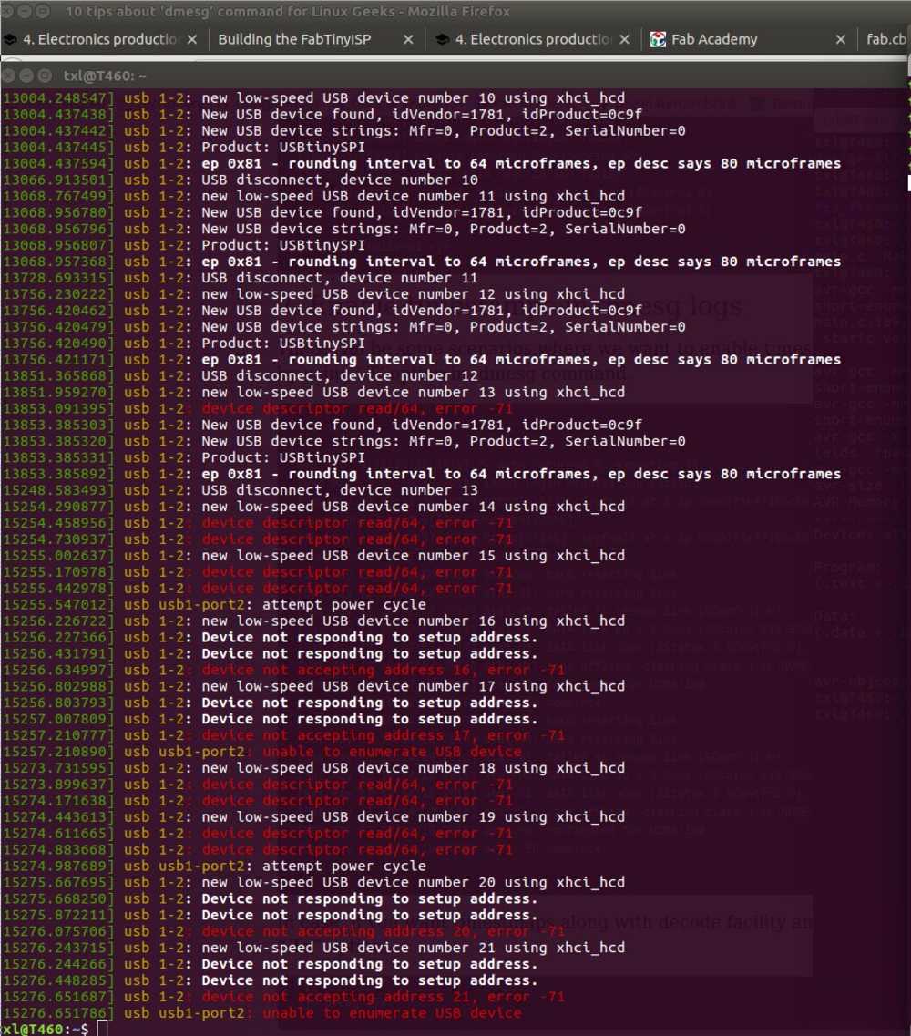
I looked up the dmesg error on the internet and found one answer on paulphilippov.com. It says the device consumes too much power and the computer refuses it: ‘USB has an over-current protection, which gets triggered when power consumption from the port is too high.’ That means something may be wrong with the electricity.
resistance meter
So I started testing the circuit for shorts. That is to say: the board has several circuits on it. Electricity should flow at each point of the circuit. You measure the circuit with a resistance meter. Place the meter on the Ohm setting. The meter should now produce its own low current. Put the two pens together to test: if it beeps it means it works. Now choose a circuit. Place one pen in the beginning and place the other pen further down the circuit. A beep means that there is a circuit and electricity is flowing. Leave the first pen where it is, with the other you go a little further down the circuit. Continue till you reach the end.
You can also test for shorts by placing the pins on two circuits that should not connect. Beep means there is a circuit and that something is wrong.
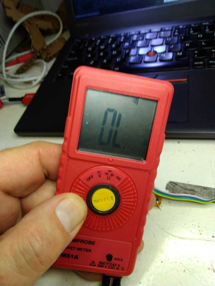 Use a resistance meter to check if the electricity current in your board is going the right way. Place the meter on the Ohm setting. When you touch two points that have electricity running between them, it will beep. If there is no current it stays silent.
Rinke had a nice schematic that I borrowed. It shows each of the circuits on the board. Each colored line is one circuit where electricity should flow through.
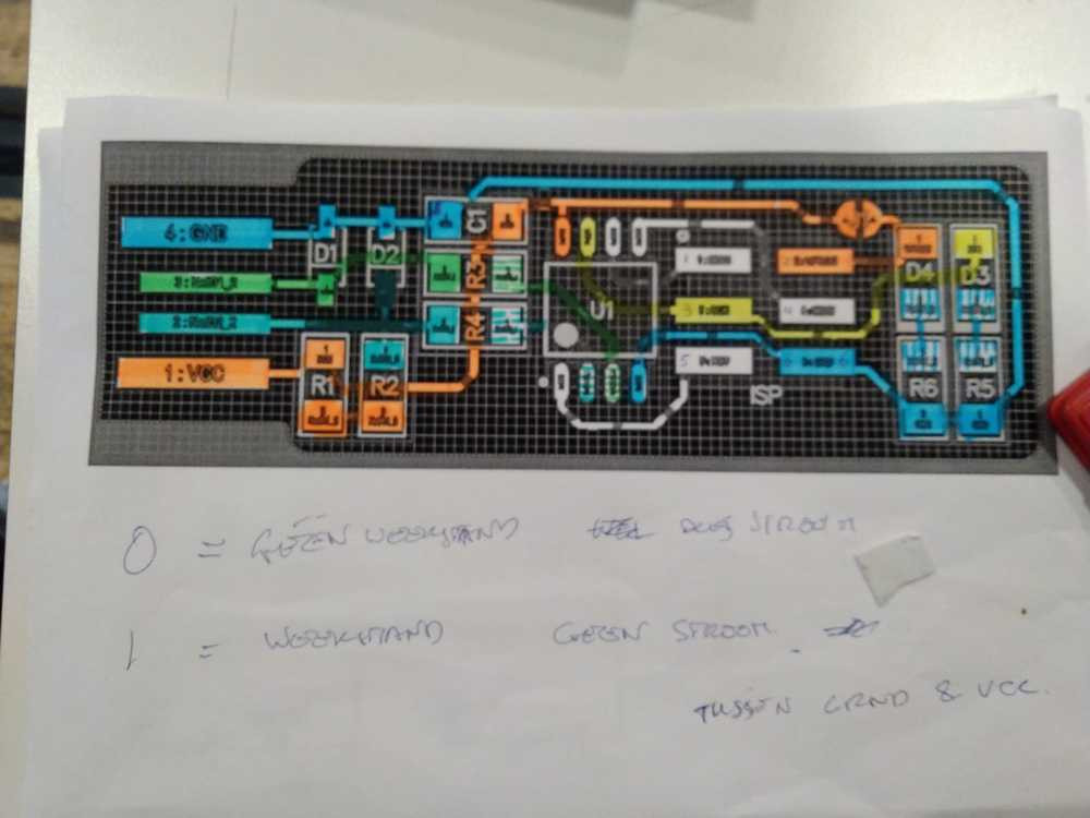
First I only tested the circuit running from the VCC pin (this is the pin where power flows through when the USB is connected to a power source like your computer.) I thought you could only use the resistance meter on a circuit that’s on the VCC. Now I understand that’s not at all how it works. As I described above, it is the meter supplying the power. You can run it through all the circuits and test them.
My ISP did not get power on the lower R1 & R2 components. But they are highlighted in the schematic above. So I thought this was what was wrong. But that turned out not to be the case. Looking at the symbolic representation of the board from the documentation page, I couldn’t tell if there is supposed to run a current there.
 Representaion of the board from the documentation page.
But Henk pointed out that on the printed board you can see R1 and R2 on the lower side are not connected. Hence, it is not an error that the multimeter did not measure a circuit there.
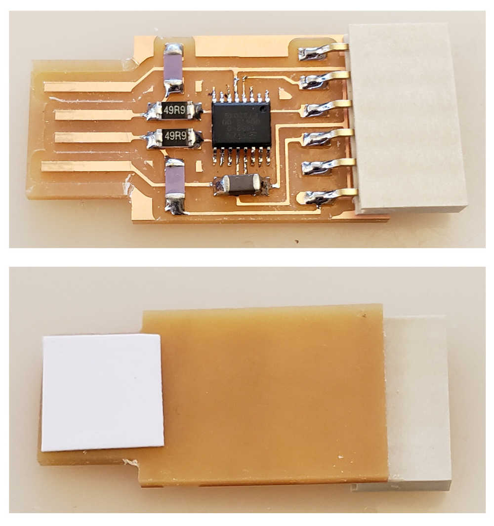
 Picture of printed board from the documentation page.
You can probably also tell that from the electronics schematic which is provided on the documentation page as well. But I don’t know how to read those yet.
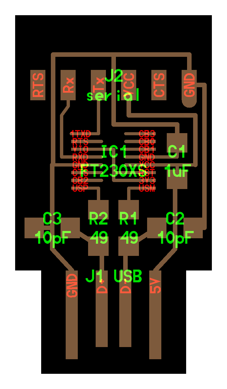
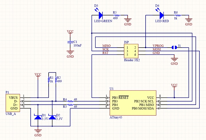 Schematic from the documentation page.
It turned out that faulty circuits were not the cause for the dmesg error message.
Checking the soldering
Henk helped me debugging. He thought the extra solder on the USB traces might be too much and piling to high. So he took a file to rasp some of it off.
A bold idea that I could appreciate. Test All The Things! But this too wasn’t the problem. In fact, some of the copper tracing was filed off as well. Henk redid it with solder. So now I know that you can replace copper with solder.
 Making sure the traces of solder dust are gone so that they don’t make a short.
The dmesg kept throwing errors. Henk thought it might be the two blue LEDs because blue LEDs consume more energy than other LEDs.
I tried going back to the earlier setup of connecting a programmer, to see if maybe I could reflash the device. That maybe blowing the fuse had not worked. But this too was a dead end.
The solution
Finally Henk found out that I used the wrong resistors. I used 499K instead of 499 Ohm. That’s a couple of orders of magnitude too much. You can see it on the resistors lettering: it says 4992. The 2 means 2 zeroes. The right resistor reads 49R0.
 You can see the 4992 resistors.
 Desoldered resistors.
After that the FabTinyUSB worked!
TinyUSB in action
In week06 the TinyUSB was put to work. Using the Arduino IDE I used the TinyUSB programmer to program the Echo board I made.
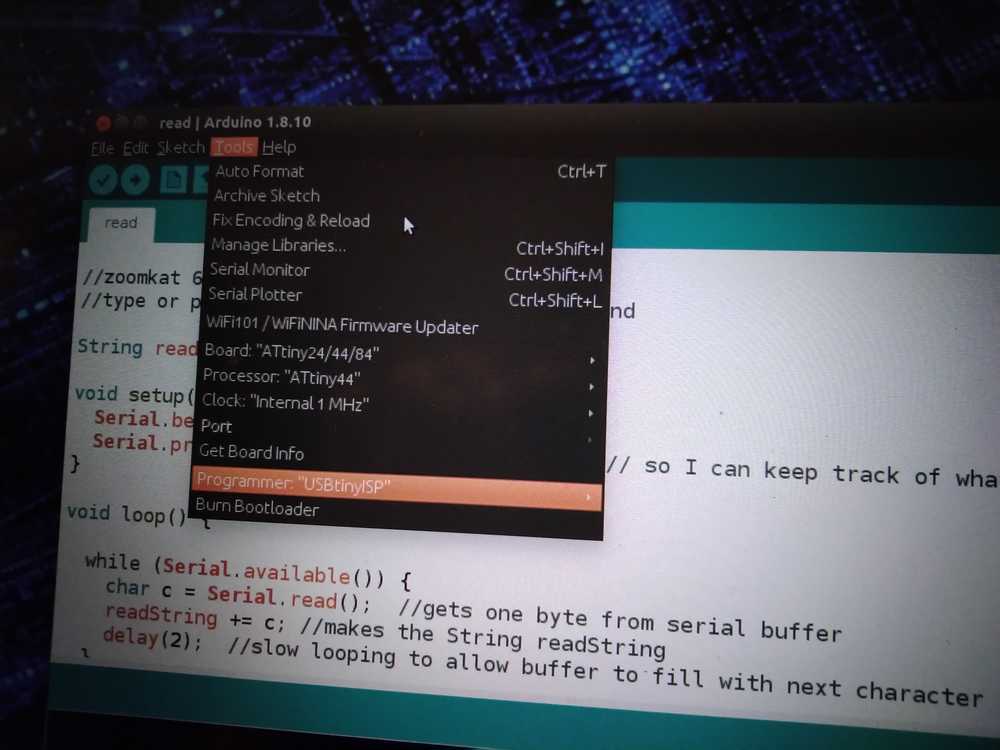 Here are the settings for the Arduino IDE.
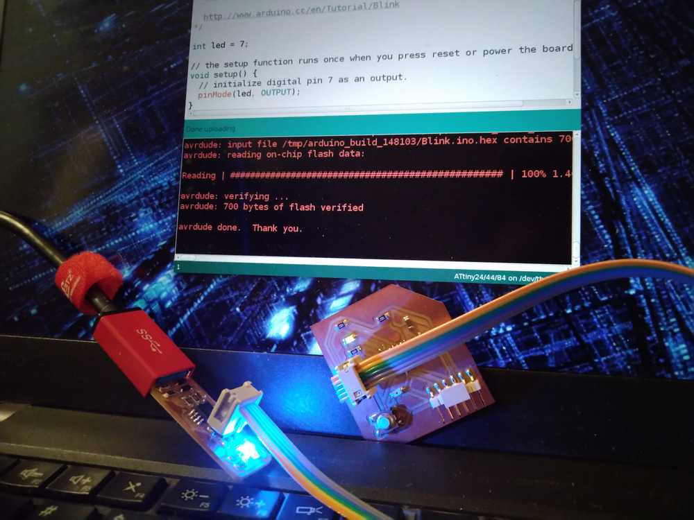
I uploaded a Blink program which can be found in my source files table of week06.
Here you can see the tinyUSB connected to the Echo board. It has just programmed the Blink program on the Echoboard. And the Echo’s LED is blinking.
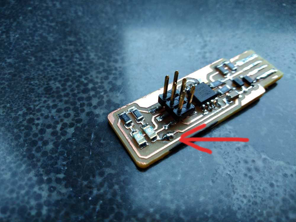
Special note on J1 bridge
We made the TinyUSB based on this explanation page. It describes the steps very precisely. One of the steps is removing the J1 bridge. This is a blob of solder that is added to the board. It connects two traces. The VCC and the Vprog traces. The explanation page states that the bridge should be removed after programming. You do that by heating up the solder and either sucking it away with the solder sucker or use the desolder lint.
However, we skipped this step. Our mentor made an TinyUSB before teaching this class to us. In his case the TinyUSB stopped working after removing the bridge. He therefore told us to leave the bridge on the board. Which is what I did.
Here is an image of my board with the J1 bridge visible.
More on the J1 bridge
For the global review the J1 bridge must be removed for this assignment to pass. There are two sources I was asked to look at: This page explains what the function of every component on the ISP is. I will refer to it as the ‘Explainer Page’. Second, there is the page we used to make the ISP. I will refer to this as the ‘Maker Page’.
They each give a different reason for the existence of the J1 bridge.
Different reasons for the existence of the J1 bridge
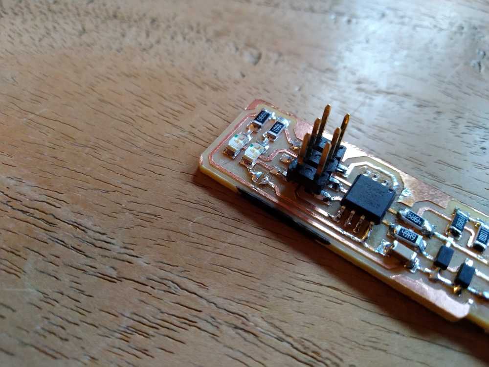 J1 bridge removed. A.k.a. the blobless tinyISP
The function of the J1 bridge according to the Explainer page:
Two different reasons are given for the existence of the J1 bridge. This is the reason given by the Explainer Page. This page explains what the function of every component on the ISP is. About the J1 bridge it says:
The J1 bridge is either made by a blob of solder or a 0k resistor. When making the board you put on the J1 bridge. Having J1 on the board enables another device to program the ISP. By programming it you turn the ISP into a programmer that can program other boards. Once you’ve programmed the ISP you want to prevent it from ever being reprogrammed again. Therefore, after the board is programmed you want to remove the ability to reprogram the board.
The Explainer Page says that the function of the J1 bridge is to prevent reprogramming the board:
To program the ISP, its RESET pin must be pulled LOW. Therefore the default state of the RST must be HIGH. When the programmer is connected to the ISP it must be able to pull the pin LOW. This is accomplished by connecting the RST pin of the AtTiny to a pull-up resistor. It is also connected to the RST of the ISP header.
So this is the reason why the J1 bridge is there in the first place: in order to program the ISP RST must be pulled LOW and this is done by connecting to the pull-up resistor.
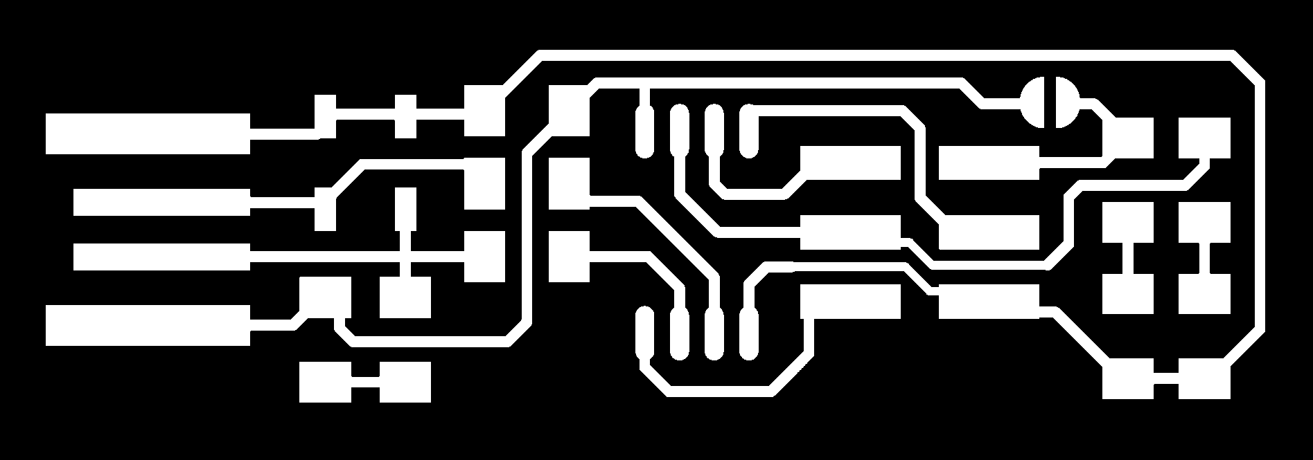
This is the traces file of the Explainer Page:
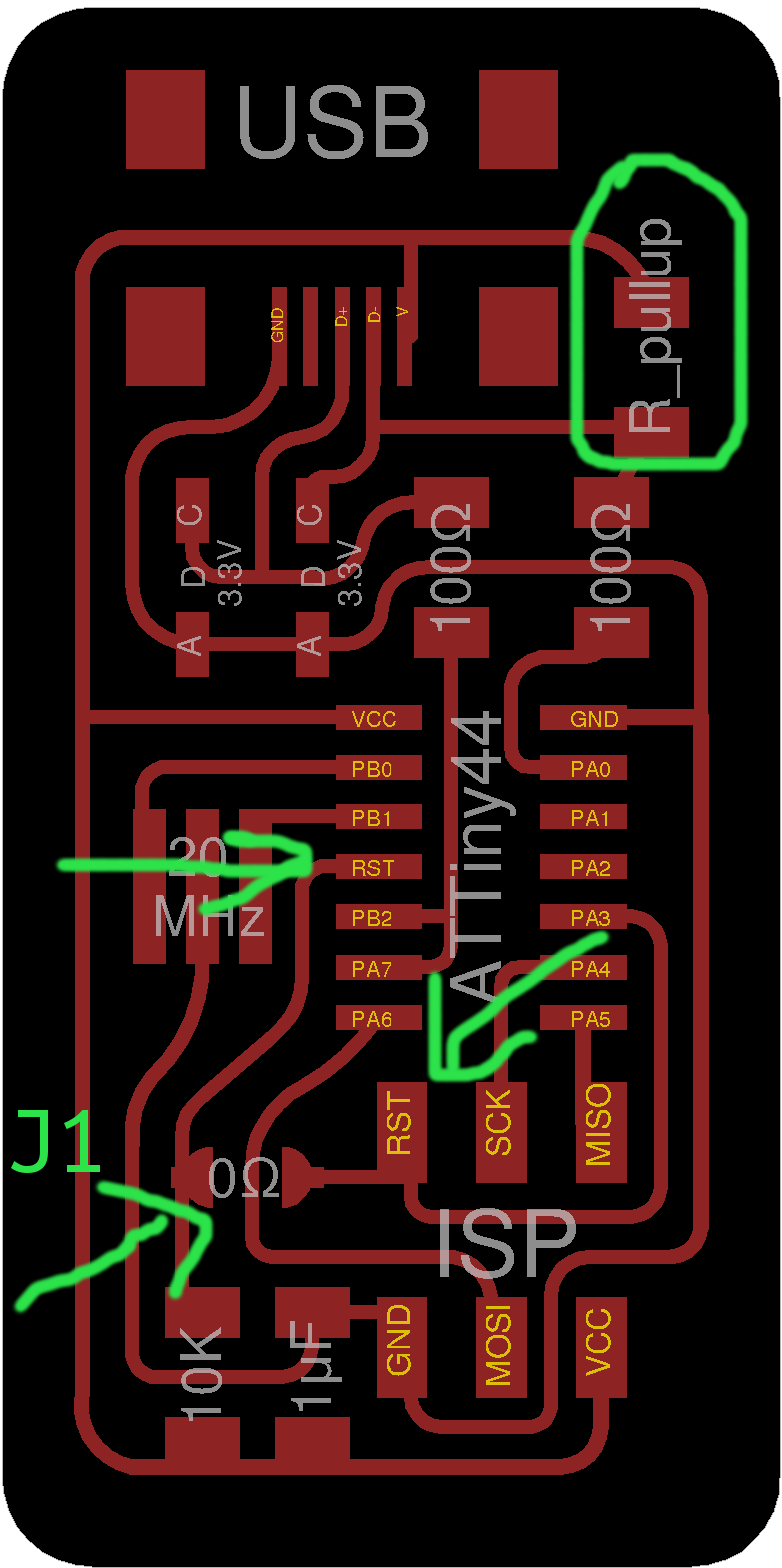 The arrows point to the pull-up resistor, the RST on the ISP header and the RST on the AtTiny. J1 is also marked. Source + my markings.
So, why remove the J1 bridge? The Explainer Page ties the J1 bridge to disabling the ability to reprogram the TinyISP. It says the J1 bridge is removed in order to disable the ability to pull RST LOW. When the bridge is removed the ISP can no longer be programmed.
The function of the J1 bridge according to the Maker page:
The Maker Page gives a different reason for removing the J1 bridge. It accomplishes that in a different way. Quote: “we need to disconnect VCC from the Vprog pin on the ISP header by removing the bridge on the solder jumper”.
When you compare the two board files, you can see that the different reasons for the J1 bridge are also visible in how they designed the boards.
This is the board file from the Explainer Page: the J1 bridge connects RST on the ISP header to RST on the Attiny.
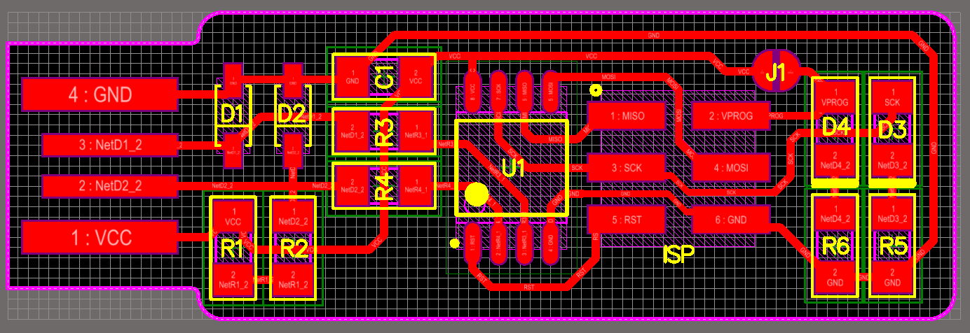
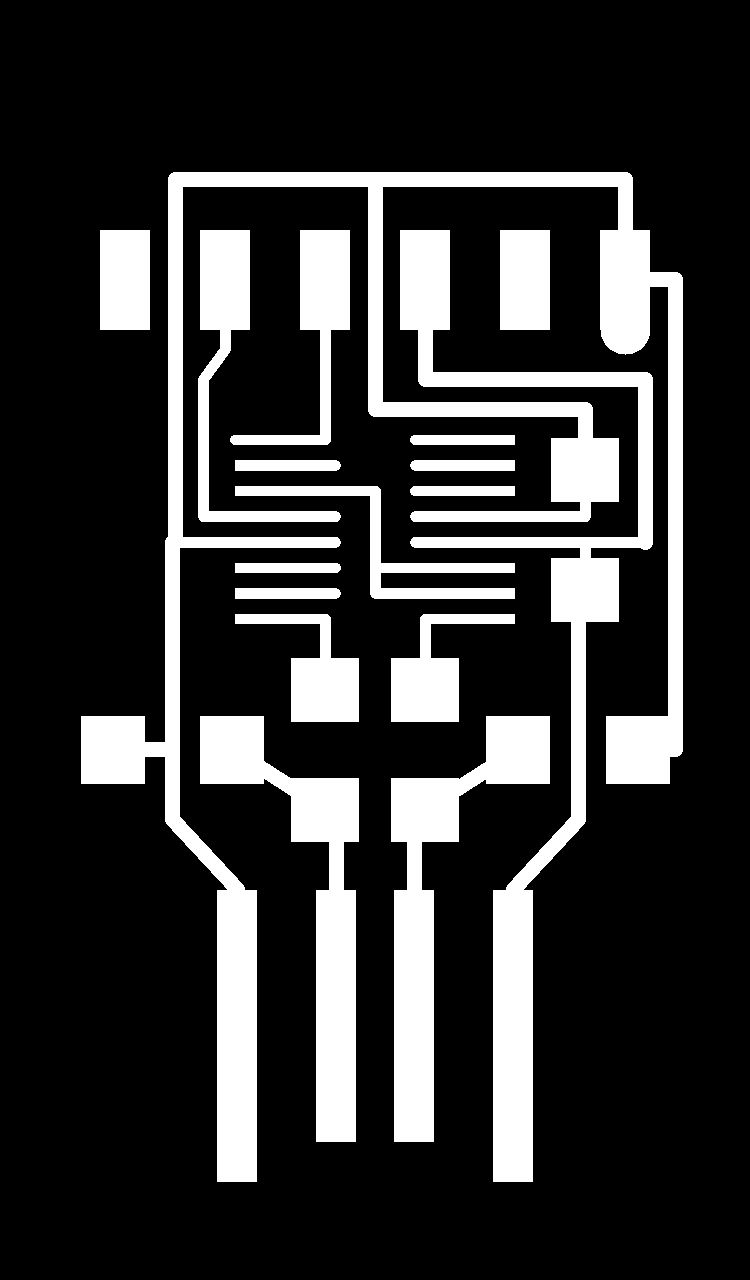
This is the board file of the Maker Page. The J1 bridge connects Vprog to VCC.
The Maker Page does not use the J1 bridge to disable the function to reprogram the board. It states that it accomplishes that by blowing the fuses. quote from the Maker page: “we need to change the bit that will turn the ATtiny45’s reset pin into a GPIO pin. Once again, this will disable our ability to reprogram this ATtiny45 in the future, which is why we wanted to make sure everything was working before doing this. Connect your ISP programmer to your board one more time, and run make rstdisbl. This does the same thing as the make fuses command, but this time it’s going to include that reset disable bit as well.”
The Explainer Page does not use the J1 bridge to disconnect VCC and Vprog. Instead, it tells you to remove the J1 bridge to prevent reprogramming and to cut the trace running from the VCC pin to the ISP header. From the Explainer Page: “After you program the board, you must remove the 0Ω resistor, and you must also cut the trace leading to the VCC pin on the 6-pin programming header.”
Why disconnect VCC and Vprog
So both sources accomplish disconnecting VCC and Vprog in different ways. The Explainer Page states why VCC and Vprog should disconnected. We are now talking about the situation after the ISP has become a programmer. When VCC and Vprog are connected the ISP supplies power to the other board it wants to program.
The Explainer Page states that this situation is undesirable. The reason: in this setup both the ISP and the to-be-programmed-board draw power from the same USB port. This could result in the USB port not being able to provide enough current to power both boards.
However, this was not the case in our situation. We were able to program the Echo board with the J1 bridge in place.
Programming with the blobless ISP
Here is proof of having programmed a board with the TinyISP with the J1 bridge removed.
 Setup is: USB cable connects to FTDI connects to Echo board connects to TinyISP.
In the back is the Arduino IDE with succesfully uploaded code. (I know your not supposed to plug in the ISP naked into the USB port but I do not have two USB cables.)
ISPtiny programming Echo board from Tessel Renzenbrink on Vimeo.
Video of programming with TinyISP without J1 bridge.
Individual assignment 2: making an FTDI
We are making an FTDI. This is a USB to serial device. Commonly this is an expensive cable but we’re making an affordable board to do this job. Most machine talk through a serial port. For you computer to talk to them you need a USB to serial converter. And that is what the FTDI does.
The documentation for the FTDI is provided on the FabAcademy embedded programming chapter. I can’t link directly to it as there are several files. Look under: host communication > FTDI > chip > hello etc.
The source files are added to the source file table at the top of this page.
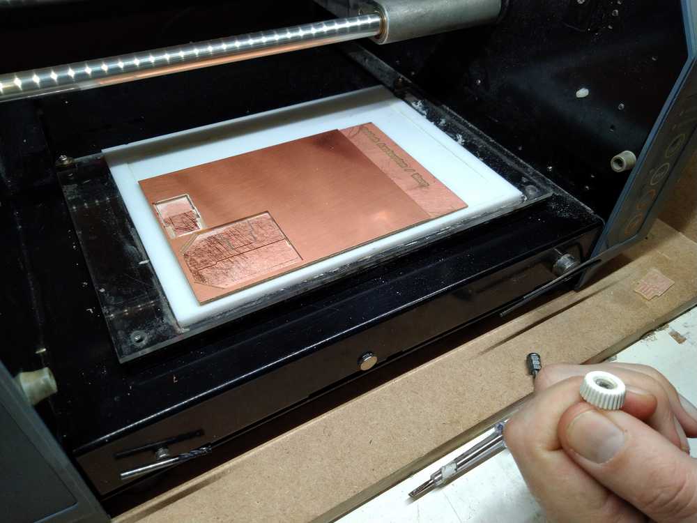
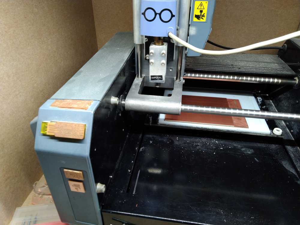
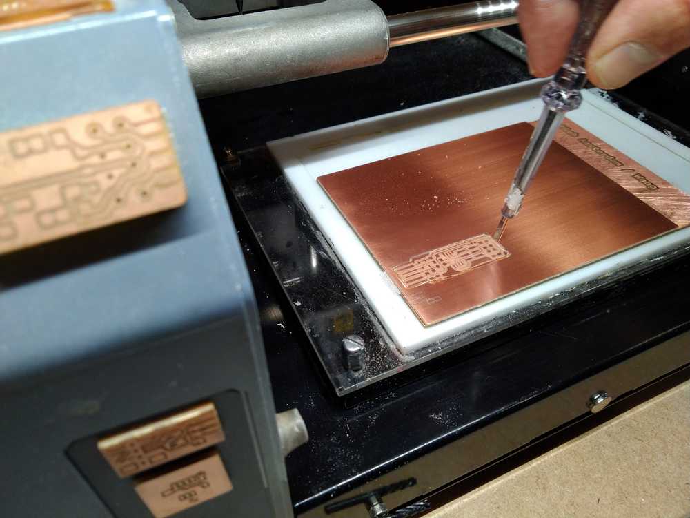
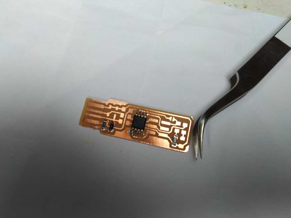
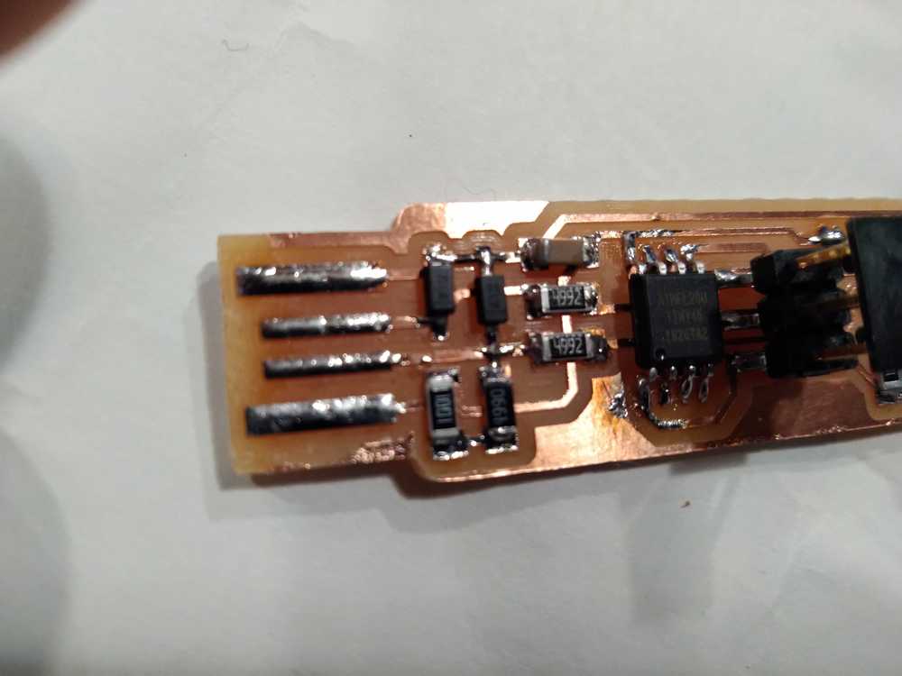
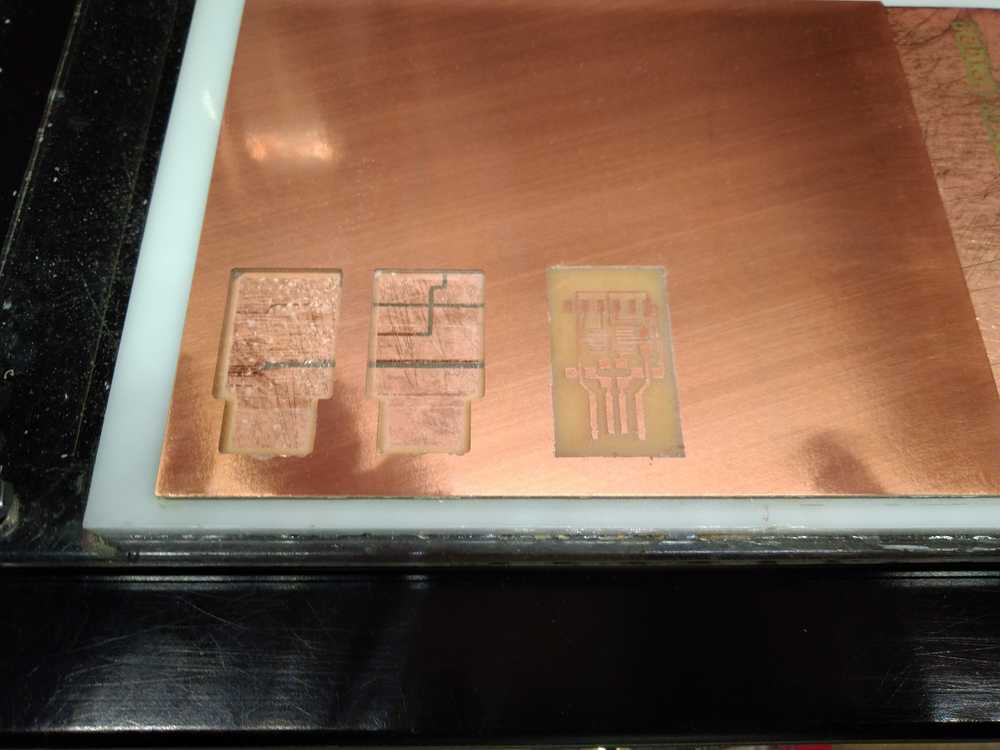
First I started on the milling machine. Uploading the traces file to Mods. The difference this time is that the offset number is set to 0. This means all the surplus copper will be removed from the board.
When the board’s traces were milled I uploaded the traces file. Using the same X-Y settings x-72 y-10.
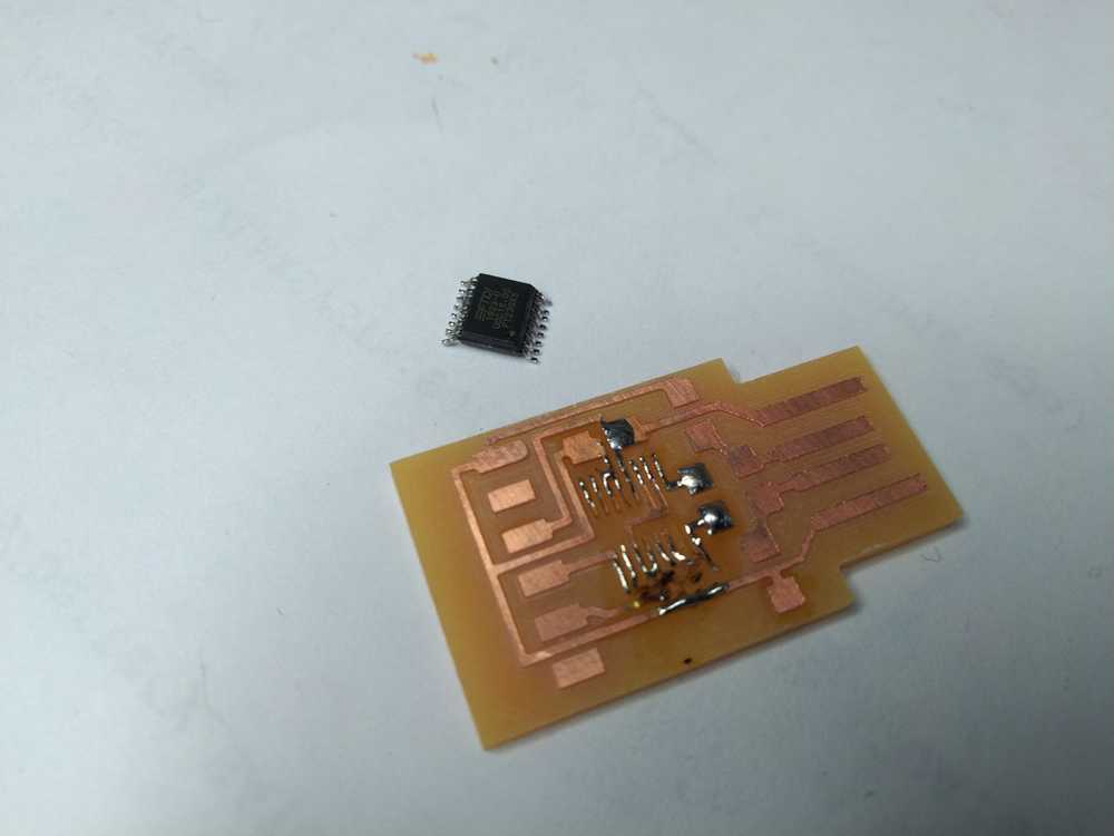
Unfortunately the traces for the IC a not entirely fastened to the board. This needs special attention while soldering.
The IC is a tiny component. Henk showed us how to solder it. First fasten 1 leg on either side of the component. Then apply solder by spreading it over all the legs. Then remove the surplus solder using the fancy solder sucker that has its own heat supply.
This went wrong as the heat sucker sucked out the copper traces. And I burned the board a little.
 Burned board with desoldered IC.
I commenced to make another FTDI board. This time I used conventional instead of climb as a setting. Henk advised that this might help against the rather loose copper traces of the first run. But the traces came out even worse this time. Some of the traces needed to connect the IC ;came loose right away. Henk said it might be the result of a blunt drill. I decided that this time I was going to make it work because I felt like a bit of a failure messing up two board. So I wanted to make new traces with solder to replace the missing copper ones. This turned out to be impossible. The board’s substrate repels solder. That is one of it’s functions. So I had to admit defeat and be a three-time board maker.
I also made another mistake. I went to make the cutout. But had failed to load the new file. The outline started then milling the outer lines of the traces again, instead of the outer line of the board. I cancelled the job. The board had partially been cut out in the middle. But since it had followed the traces, it had not yet cut through any traces yet. I thought I could still use the board. Retracing the copper traces around the indent with solder. But I haven’t found out if that would’ve worked since there were other problems with the board as well.
 Two mistakes are visible on this board. 1. There is a cut-out in the right side. 2. Copper traces are missing. Attempts to replace with solder failed.
On the third try I made another mistake. I checked the flow control, it was on the wrong setting so I changed it to RTSCTS. But I did not press Calculate and I did not close and re-open the web socket and port afterwards. That meant the changed setting did not take effect. So I added to my steps on working the milling machine to always close and re-open the ports before commencing a job.
I am now on my fourth try and make yet another mistake. I forgot to move the Z-axis up. This means the drill has no room to cut the copper. It is only engraving it because there is no space on the z-axis to move up and down. Henk advised to let the job run out and then just redo the traces again after moving the Z-ax up a bit.
X-Y settings of the fourth and fifth try: x - 117 y -10
This time the bed is not 100% vertically straight. The left side of the board has all the copper removed but the right side does not. Henk offers a solution. Place a piece of paper between the bed. This will lift the bed a couple of tens of millimeters. This time I set the offset to 4 rather then 0 to save some time.
I hit send, when the job was done nothing had happened. Forgot to lower the drill.
 The milling bed is skewed and the drill did not remove all the copper. Solution: screw a bit of paper between the bed and the machines surface. This will lift it up a tiny bit.
The paper hack didn’t work. It turned out that the FR1 board wasn’t taped properly to the bed. Someone had used too few double sided tape and the board did not stick the the sacraficial bed. The result is that it swings up and down with the drill, which, not getting any resistance, can’t mill.
A new FR1 board then. The double sided tape was spent. None to be found in the entire lab. Het to go to the store to get some. There is some kind of unfavorable streak going on here, haha. I am writing this as the sixth try, third board is milling. After that there is still the soldering that could go wrong…
X-Y settings of the sixth try, third board. X-20 Y-10
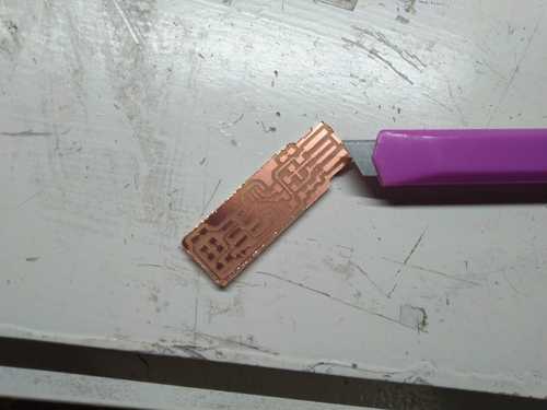
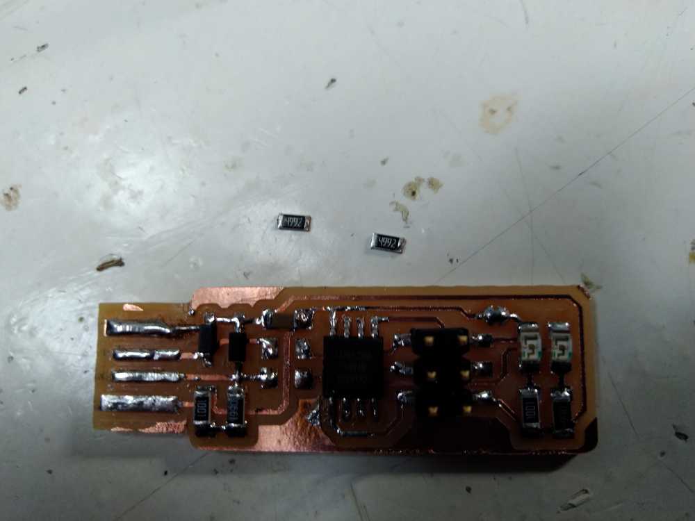
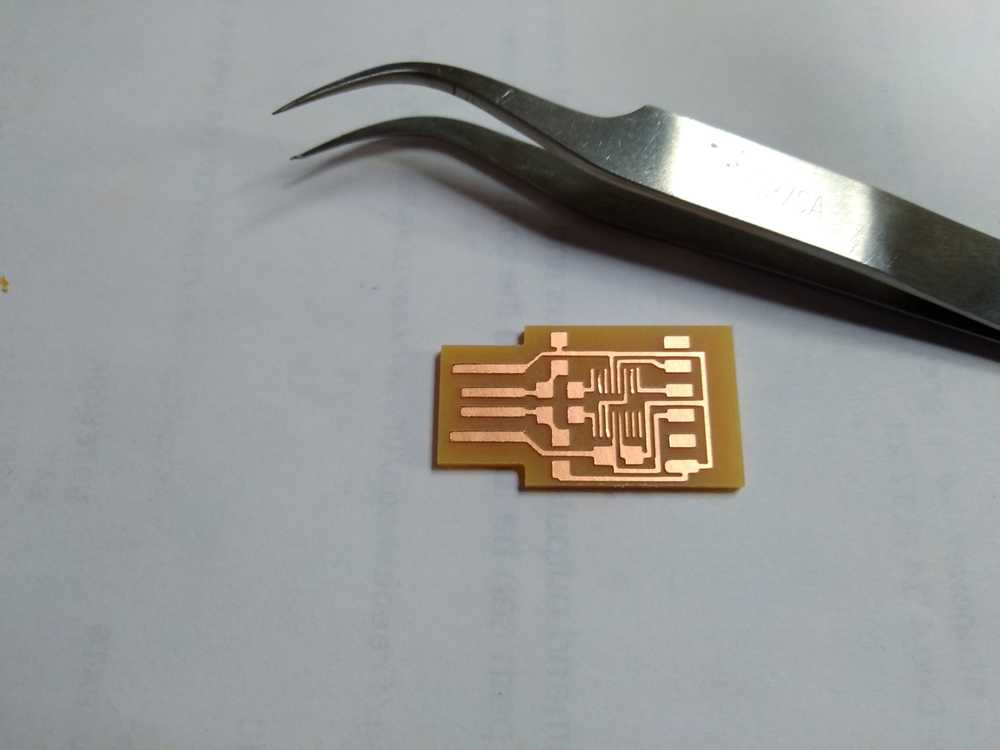
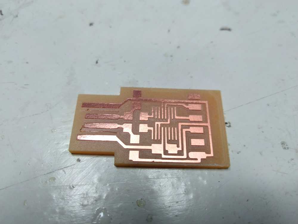 The board is finished and it came out well. The copper traces are not loose this time
Drivers
On the FabAcademy documentation page is a link to the drivers. The page has multiple kinds of drivers. It says: ‘ For most of these operating systems two types of driver are available: Virtual COM Port (VCP) drivers and direct (D2XX) drivers. The VCP driver emulates a standard PC serial port such that the USB device may be communicated with as a standard RS232 device. The D2XX driver allows direct access to a USB device via a DLL interface.’
Since we want to use the FTDI to communicate to machines over USB I choose the VCP driver.
Then I looked up the Linux driver because that’s what I run. It turns out Linux does not need extra drivers to operate this device. From the driver age: All FTDI devices now supported in Ubuntu 11.10, kernel 3.0.0-19. VCP drivers are integrated into the kernel.’
Mistakes I made
I made many mistakes this week. They are all described in detail above. To sum up: Making the FTDI board took me five tries. The first mill job went fine but then during soldering I made so many mistakes that the copper traces disappeared from the board. Not checking flow control and milling on the wrong setting. Not changing from the traces file to the cutout file before starting the cutout. Not moving the Z-axis up, resulting in to shallow a trace. Drilling with a blunt drill. The bed was not entirely straight and the drill removed not all the copper.
I soldered on the wrong component on the FabTinyISP using 499k Ohm instead of 499 Ohm.
What I liked
After the first failed solder job on the FTDI and the subsequent ruined board I felt bad. I guess I felt ashamed for making so many mistakes. First I also thought I had had a useless Tuesday. I had come in in the morning to make an FTDI board and left in the afternoon not being one step closer. The shame parameter plus the uselessness parameter made me quite frustrated. But soon I realized it wasn’t a failed day at all. I have learned many things about the milling machine. What can go wrong obviously. But also that with this machine you have to follow your documentation to the letter. I learned that I am here to learn and that a finished product (the FTDI) is but a small element in the entire process. I also learned that things go wrong but feeling frustrated about it does not help in any way. After that moment of frustration, things went wrong at least 5 more times. I am very happy that by that time I had decided not to be frustrated or ashamed anymore or it would have become a guelling proces. Now it was actually becoming quite of fun. Doing the milling over and over again getting intimately acquinted with the process.
Also, both my fellow class mates and Henk were all quite merry about all the mistakes. Rather then riduculing or getting frustrated, that was pleasant to experience.
Global lecture
At FabAcademy we look at Form and function. The next weeks we will alternate between physical fabrication and making circuits.
Every two weeks on electronics:
Making a circuit programmer.
Designing circuits.
Programming circuits.
Bring inputs into them.
Bring outputs out of them.
Group assignment: characterize the design rules for your PCB production process.
Individual assignments. make an in-circuit programmer by milling and stuffing the PCB, test it, then optionally try other PCB processes. We’ll be making a programmer to program other circuits.
Beginner mistake: you can break the end mill. Therefore follow the steps of the instructor. Fix the board with adhesive. There is an underlay layer. That is to prevent cutting into the machine bed. Place your board on the stock to avoid wasting material. Zeroing the tool. Hold head in place when screwing tight the set screw. Do not tighten the set screw too much. Debur the board: removing the access dust. Clean the board.
The setting climb versus conventional. Climg is the most often used setting. In this picture Neil shows the difference. With climb (right in the picture) the knife cuts the ‘mountain side’ of the trace into the valley. With conventional milling the knife moves from inside the ‘valley’ of the trace and cuts the ‘mountain side’ (left in picture.).
You can make circuits on the vinyl cutter and place it on any substrate. You can put it on a cube for instance. You can make a multilayer by alternating between circuit layer and mask layer. You can capsulate it in epoxy.
Window is great for high frequency, industrially done on teflon. We can do it on glass.
Layers:
via’s: holes to connect top and bottom of a board. You can use rivets to easily make them.
Octopart: search engine for parts.
Instead of breadboards we use a different workflow.
Solder
many different kinds. Different melting temperatures: eutectic
All joints ought to be shiny and smooth. Solder tip has to be small, it has to match what you are doing. Remove surplus solder. Bring it on on the intersection of both parts. Wait a moment, does solder flow. The heat must flow up the leg and down the trace. Keep iron there, to allow the solder to keep flowing.
Reflow: parts are underneath. Put solder on the board and heat up with hot air.
Drag soldering: add flux & rub the solderer back and forth.
Stuffing: putting parts down. Right orientation. Solder from low parts to high parts and inside out.
Desoldering: braid (lint): trick: add a bit of solder to get the solder flowing.
Vacuum pump: suck away the surplus solder.
Removing a part. Pick it with a tweezer. Apply heat and hold the entire board by the part. The Board will fall away.
This week I worked on defining my final project idea and started to getting used to the documentation process.
CAM
This week we get the design for the circuit. Gerber format is historical. We use bitmaps. We work with 1000th of an inch. You can view it and make small correction easily. Picture you use must be at the resolution of the screen.
Group assignment: what is the skinniest trace you can make.
indiv: make and test programmer: extra credit: try vinyl cutter.