15. Networking and Communications
This week we learned about and practiced networked communication between nodes. Group assignment and personal assignment kind of blended together as we were connecting a number of self-built and commercial nodes to each other on an I2C bus.
Group Work
A detailed documentation of our group assignment work can be found on the shared group assignment webpage. I had never used I2C communication between microprocessors before, just to communicate with sensors and other peripherals, so this was a very useful exercise. Another very important lesson learnt was that the Serial communication TX and RX LEDs on the Arduino Nano are actually not connected the same way as they are on an Arduino Uno, which threw us a big curve ball when trying to debug things - they do not blink whenever the hardware UART is in use, but actually only light up when the USB-Serial converter is sending or receiving.
Individual Work
This week 15 was the second week of my Covid infection and isolation, meaning that I could only return to the lab a few days before assignment due date to work on the Networking topic. Upon returning to the lab, I found that my colleagues felt very challenged by the topic at hand, so I made it my focus of this week to try and explain the basic concepts of I2C communication (as that is one of the more useful ones when talking to sensors and/or between boards) to them as good as I could.
Building a Network
To that end I decided to set up a slightly larger network than just two nodes, to emphasize the point: that the network could be flexibly sized and the setup was very simple due to all nodes simply being connected to the same bus.
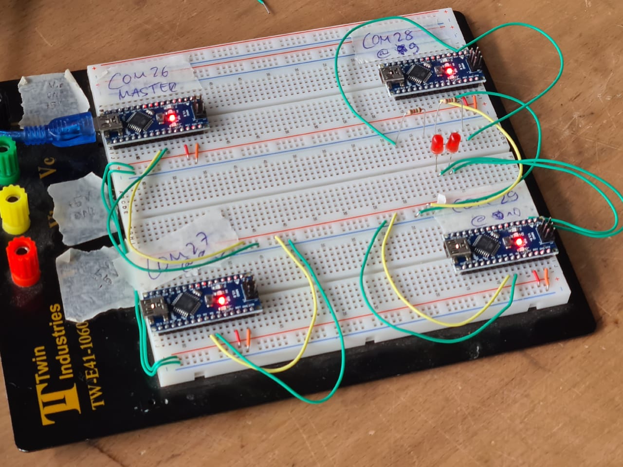
I started out by arranging four Arduino Nanos on a large breadboard, so we would have enough space to arrange the nodes in very similar ways. Spacing them out that far was deliberate to emphasize the network aspect of things. I started out by wiring all nodes to a common power bus:
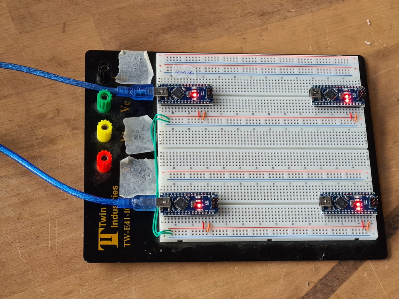
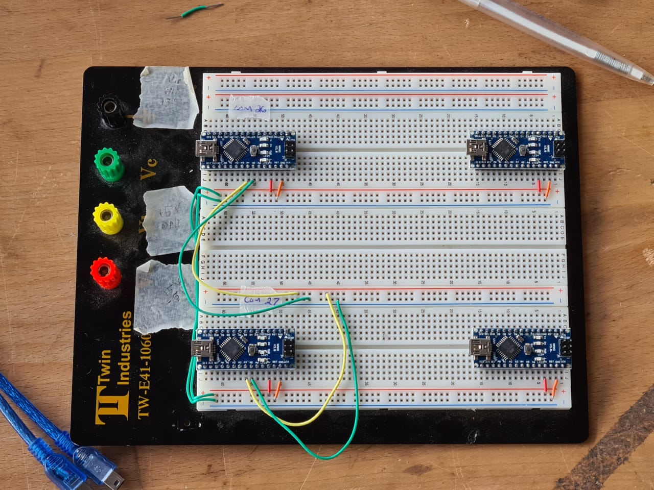
After that, I started wiring up the nodes to common I2C SDA and SCL data and clock lines. To emphasize the idea of this being a bus and not a point-to-point network, I used one of the breadboards middle, unused power bars to carry the SCL and SDA signlas across the breadboard:
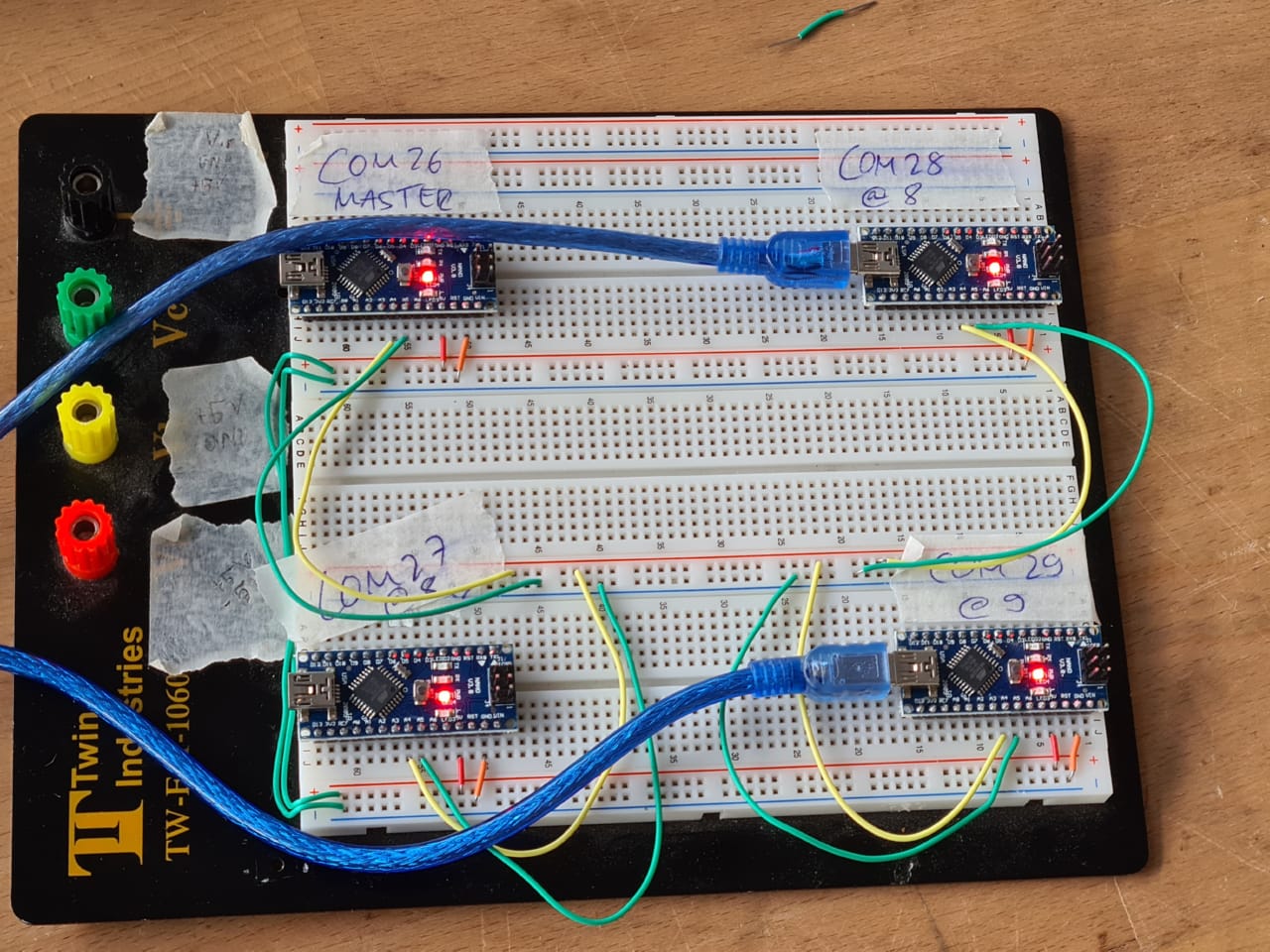
After connecting all nodes to the bus, some major relabeling was performed to keep tabs on who was master and secondary and which addresses the respective devices had on the bus:
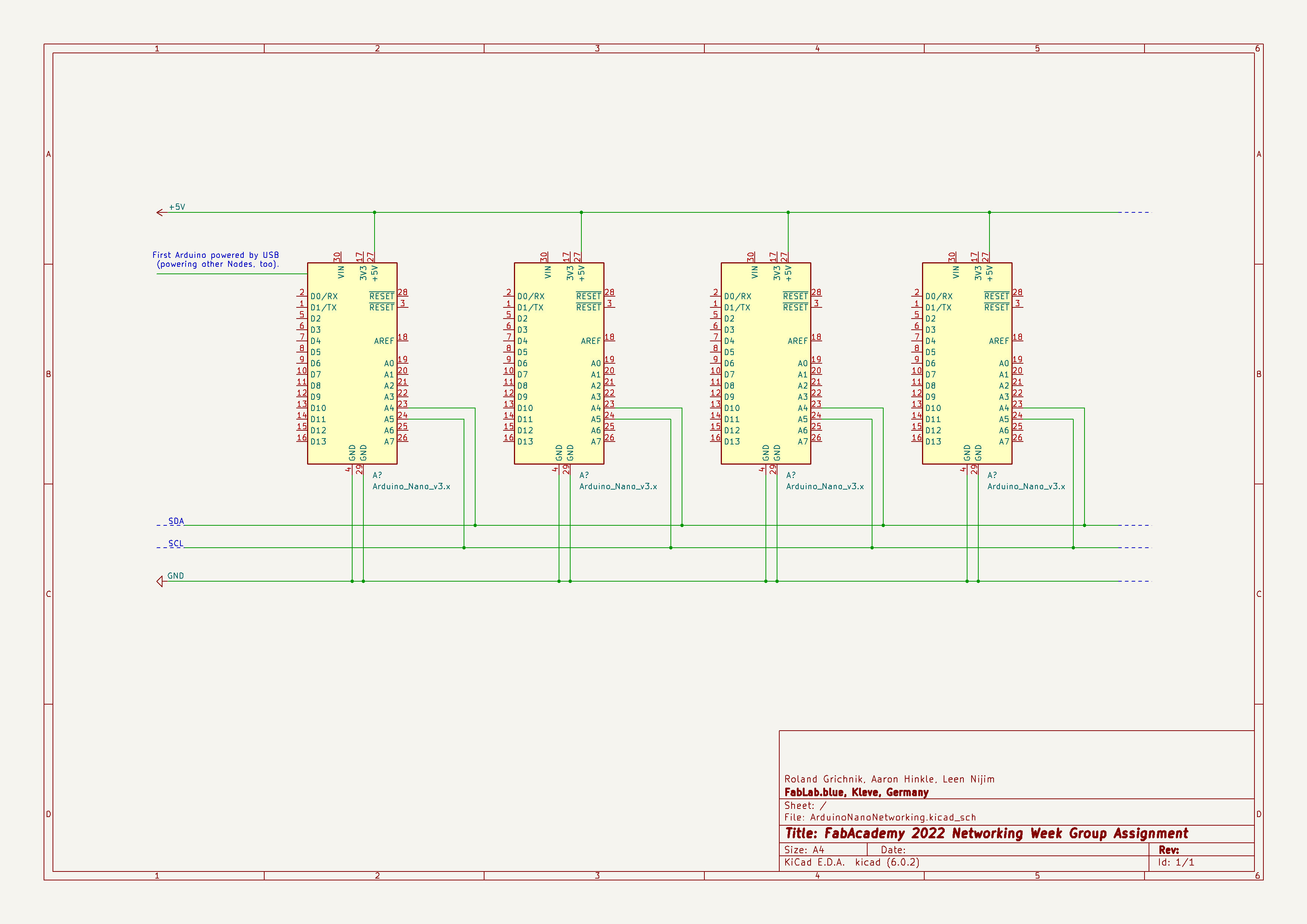
Here is the basic schematic for how the Arduino Nanos were connected. Since this is simple bus communication, the Arduino Nanos’ hardware I2C pins were connected all to the same bus, as well as power. Only the first node was powered via USB and powered the other ones with it:
Between two secondary nodes, I also set up a little direct connection via UART. This was mainly to illustrate some key differences between the direct endpoint-to-endpoint UART connection and the more open bus network communication in regards of setup, communication and programming:
Here, some direct communication via UART can be observed between the two secondary nodes (by the flashing lights on the data lines), while the nodes also participate in the I2C bus communication:
Finally, the master node was programmed to cycle all secondary nodes’ LEDs on and then back off again, just I2C bus communication with recipient addresses:
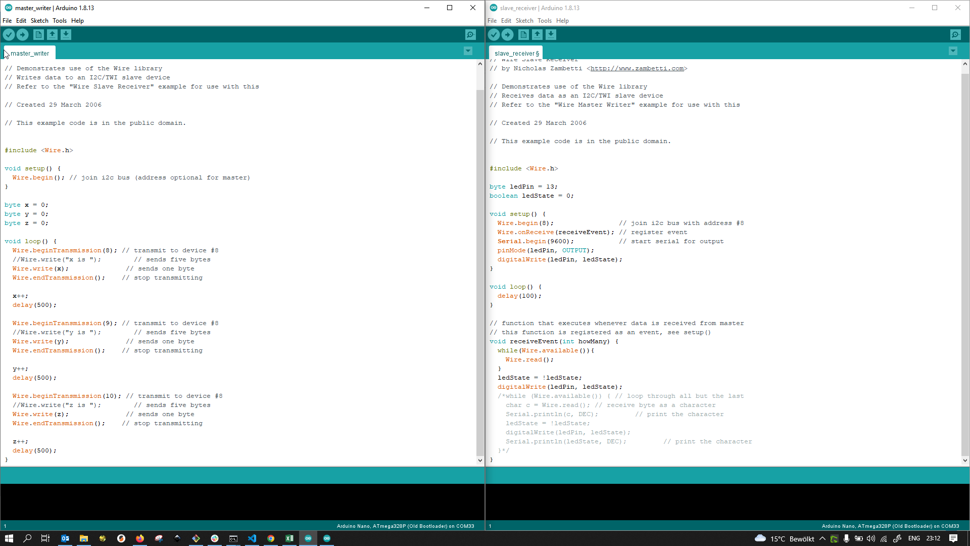
For this general, big Arduino Nano network, I used the sample code from the Wire library in Arduino IDE and slightly changed it. The master was just uploaded to one node and would send garbo data to devices at addresses 8, 9, and 10. All the while, the secondary code that was uploaded to the three secondaries was changed slightly for each node so that they initialized as addresses 8, 9 and 10, respectively. Upon receiving data (the actual data didn’t matter, they toggled their LED state. The master node would simply cycle through all the recipients, thereby flipping all their LEDs sequentially:
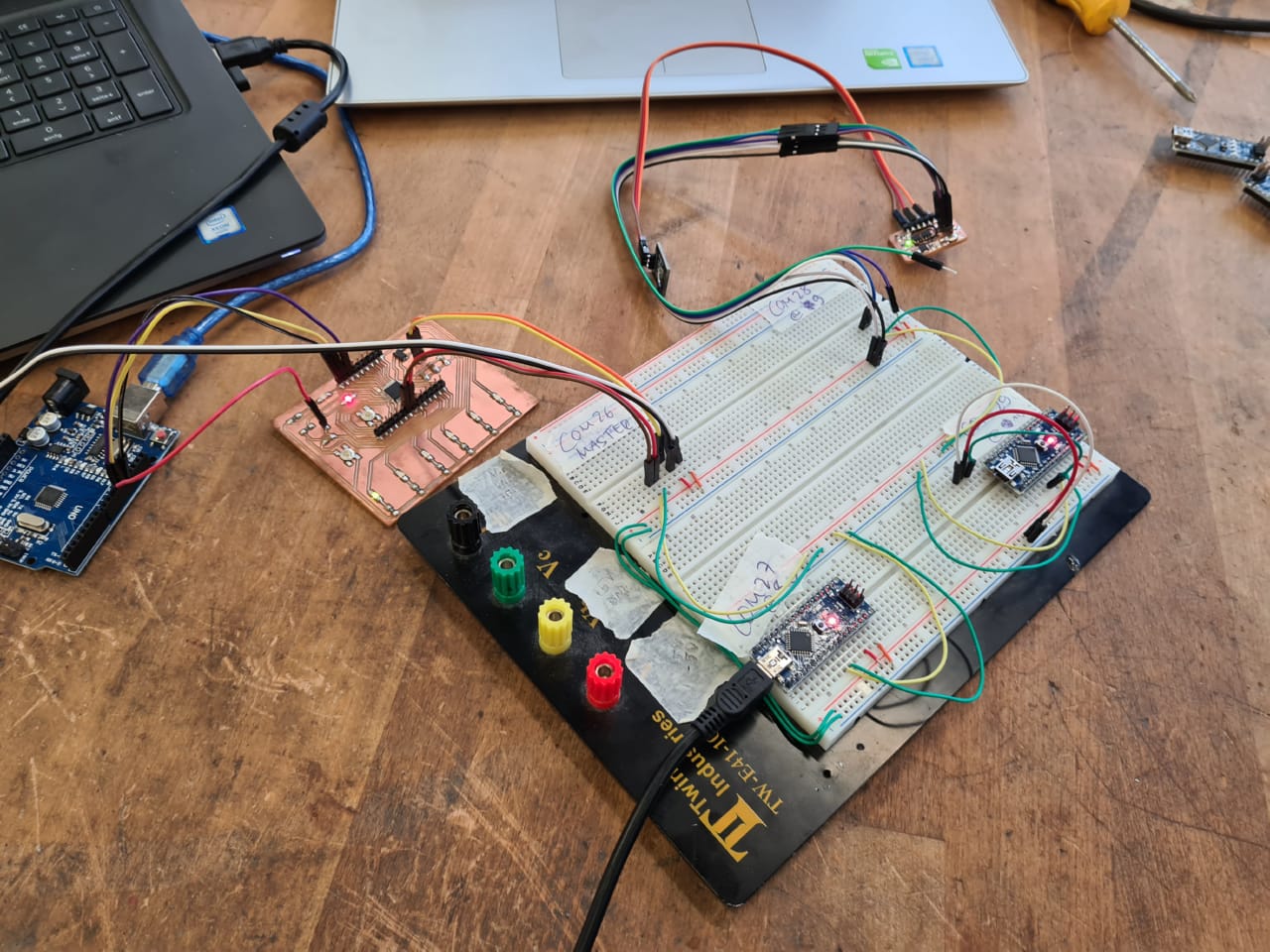
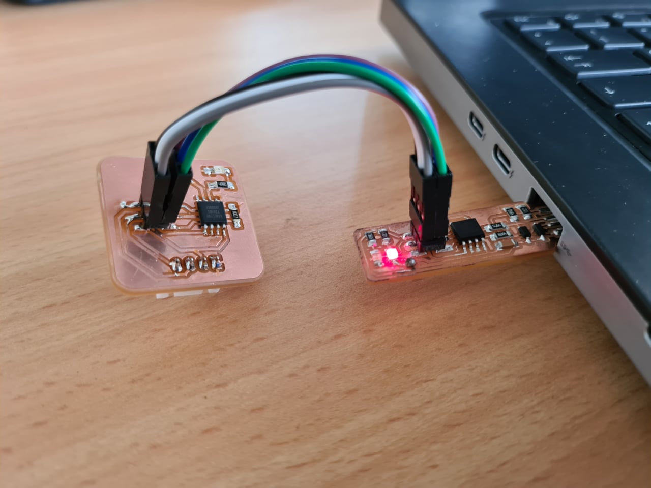
To spice things up, Aaron and I teamed up to join our project boards on the bus, too. A beginning was made by connecting Aaron’s Satshakit board (and the accompanying Arduino as an ISP programmer) to the breadboard as a secondary node (yes, the label on the breadboard is inaccurately saying Master at this point):
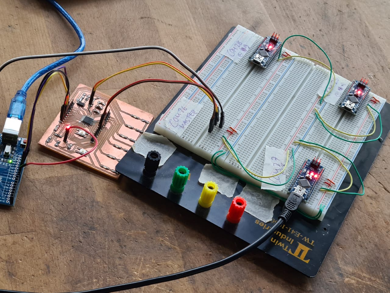
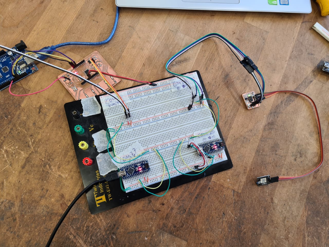
This was followed by adding my very own ATTiny44 FTDI Echo board to the bus, too. The firmware was running the TinyWireS library for providing I2C functionality:
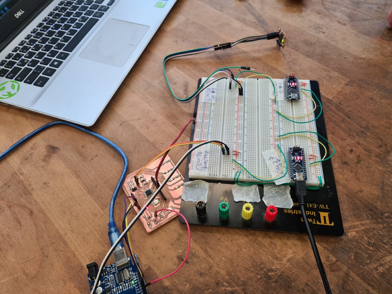
I then added a sensor to my little node that would be polled from a master node. I chose an analog hall sensor that would be able to return the distance to a magnet:
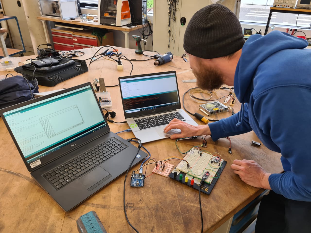
Aaron Hinkle at work uploading things to nodes:
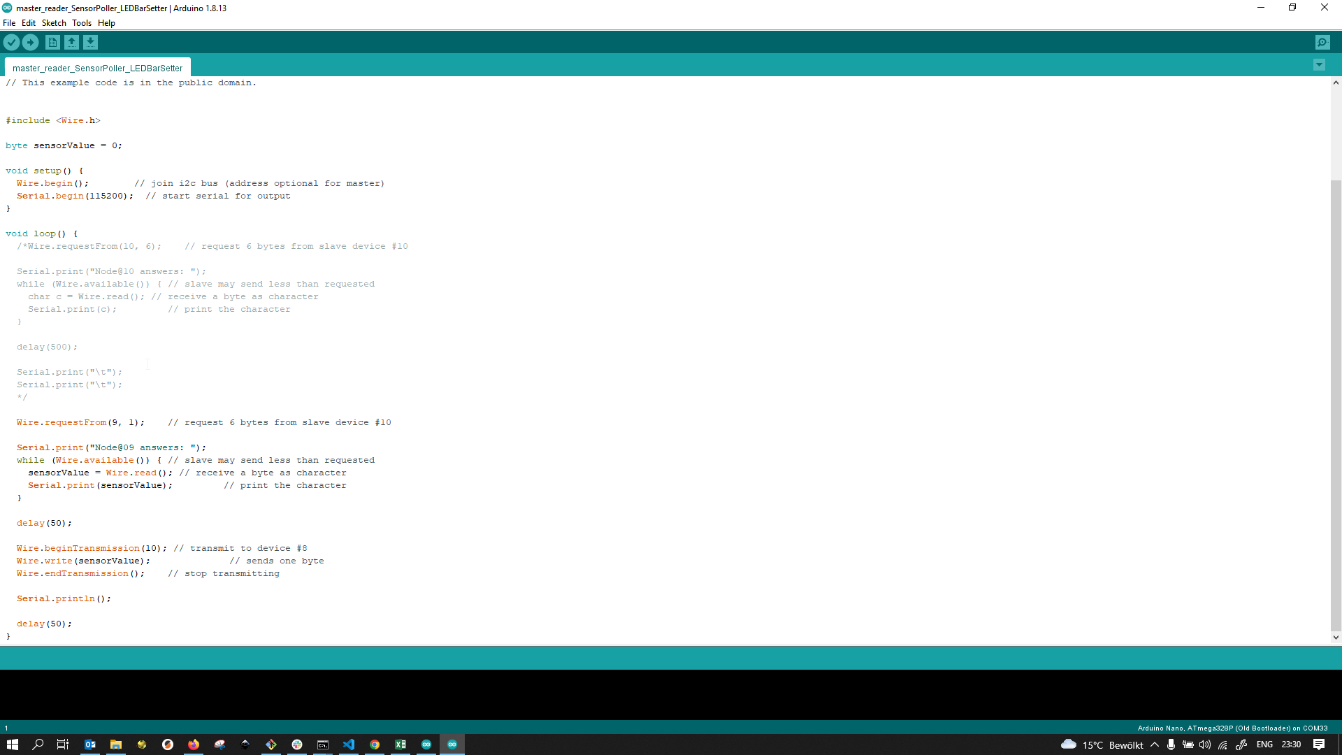
And in the end, we had an Arduino Nano master node that would request data from my ATTiny44 FTDI ECHO secondary node, which would then read the analog sensor data (distance to a magnet) and return it. The master node would then send the data to Aaron’s Satshakit secondary node which would display the measured intensity using the LEDs arranged like a bargraph on the board:
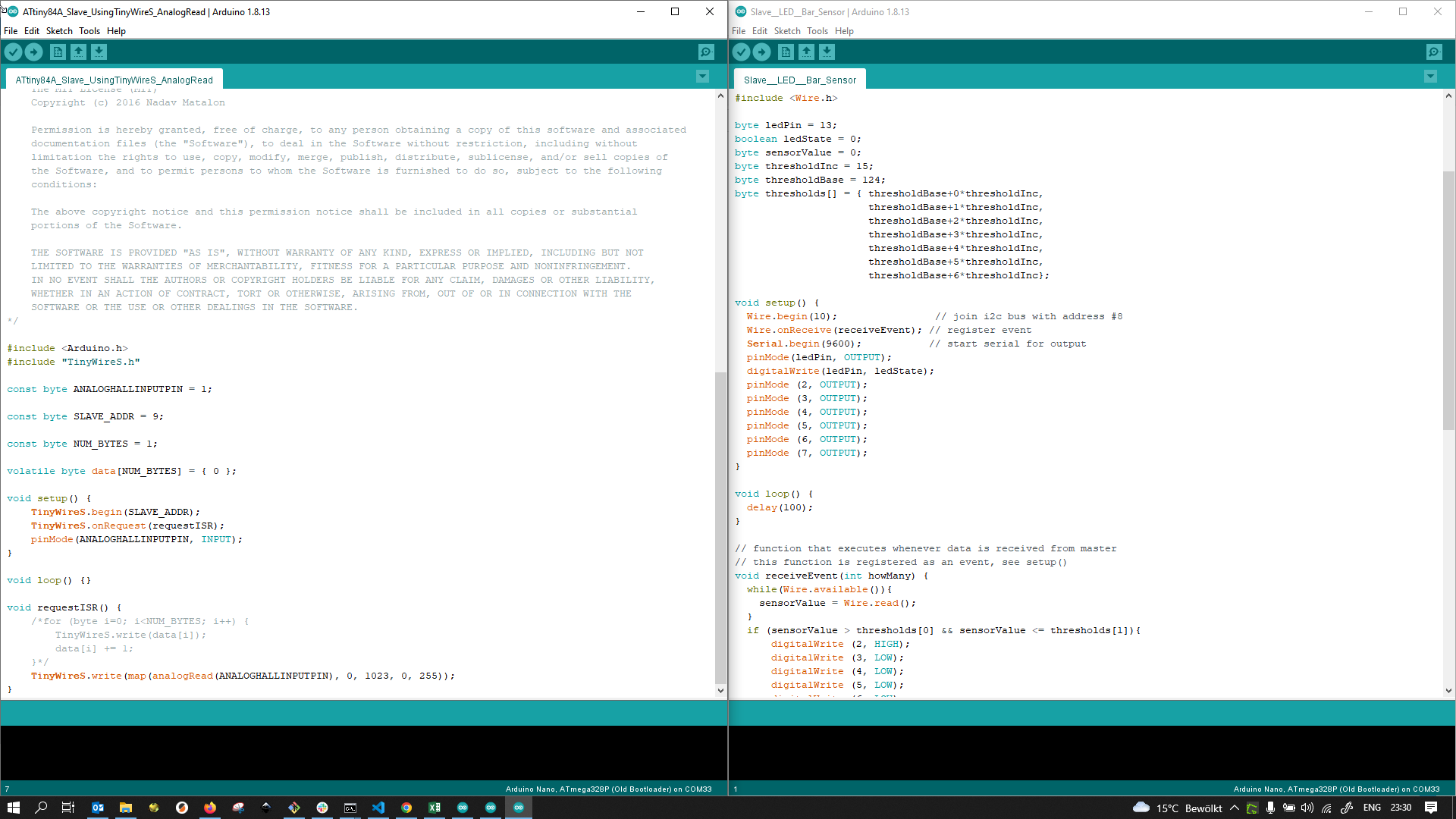
For the network that contained our own nodes, here are the two secondary’s codes. One of the is a secondary that waits for a request and when requested, returns data from an analog input. The other one is a secondary that waits for data to be received and when receiving some, sets the led bars accordingly.
The last piece of code here is the master code, which was running on an Arduino Nano and read the data from the one secondary board and sent it to the other one. All the adresses in the codes changed often, so they are not necessarily in sync. At the time of actually programming this network, of course all the adresses were properly determined:
Conclusion
This was a very valuable week. Much more than on the electronics network, we actually came together as a small network of people, transferring date (/knowledge) between one another and learning one or two valuable electronics tidbits along the way, too. It’s all about communication :)
Addendum
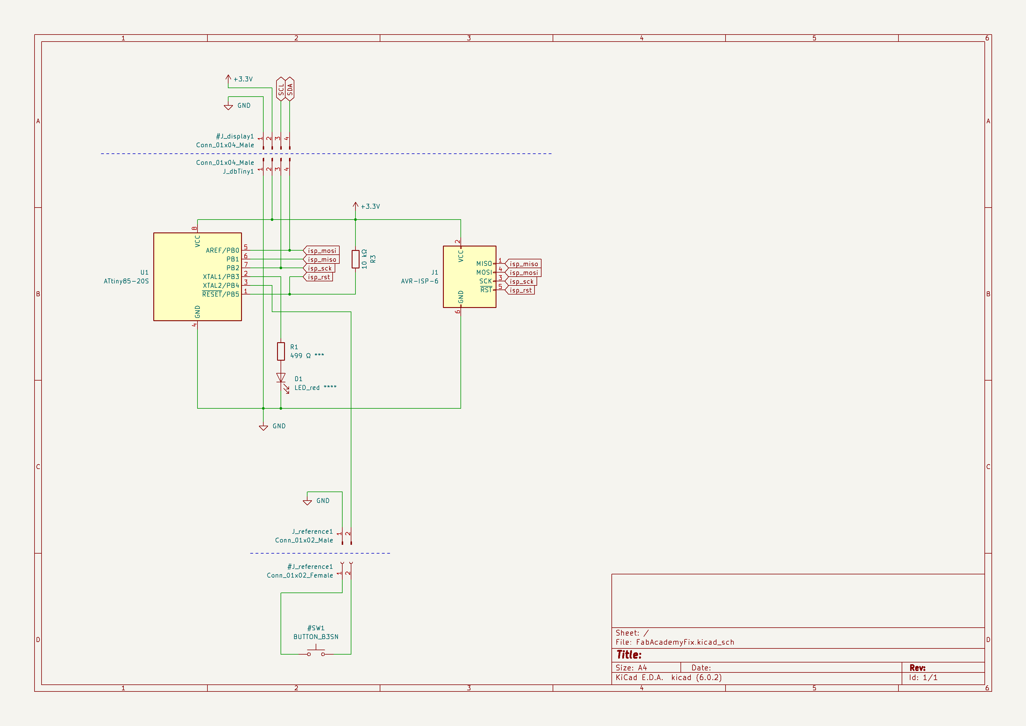
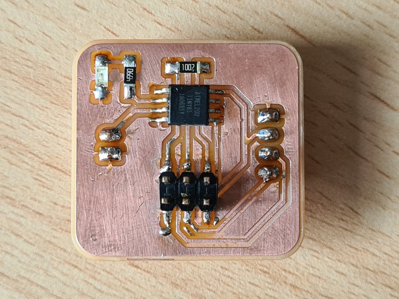
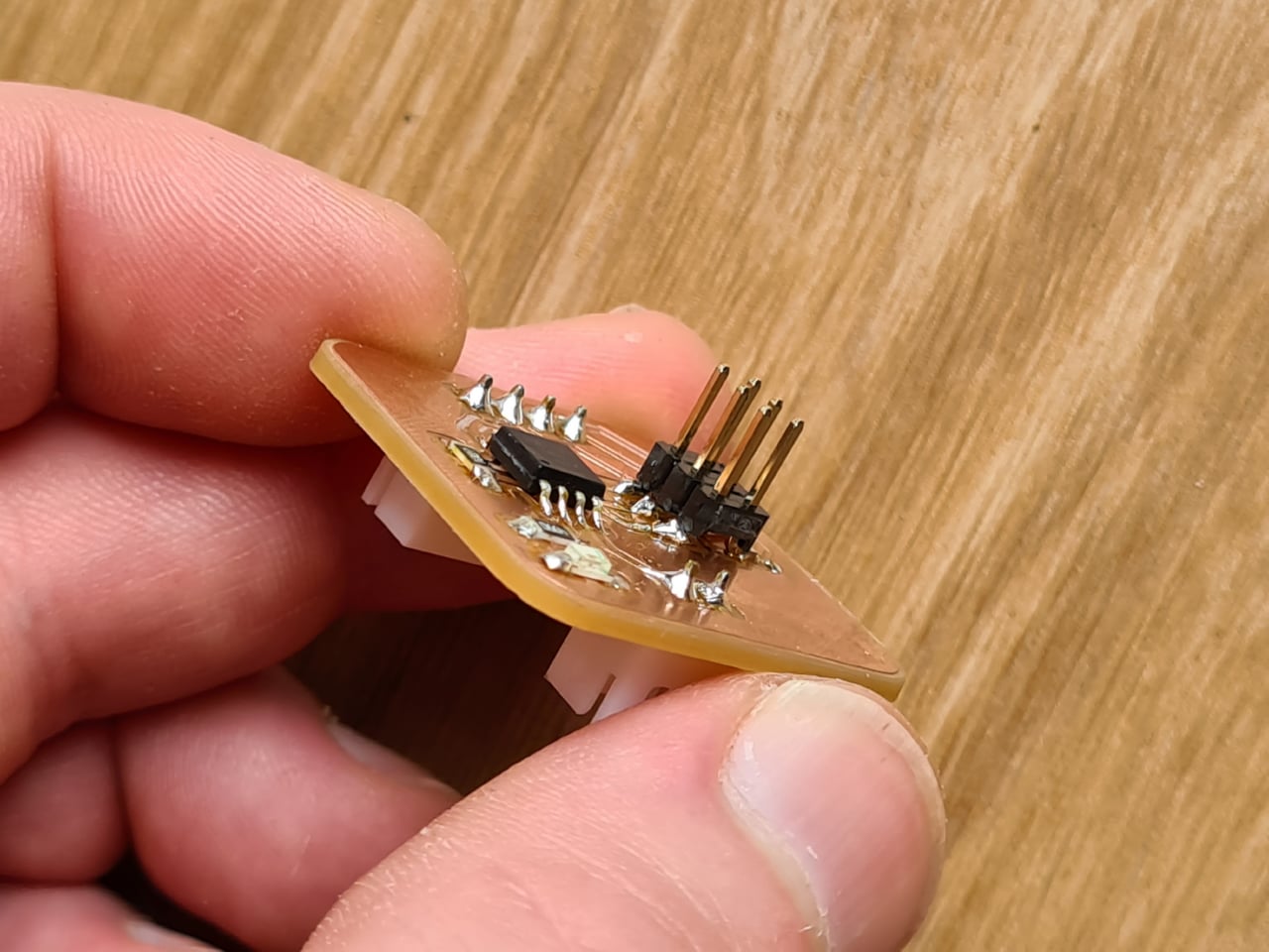
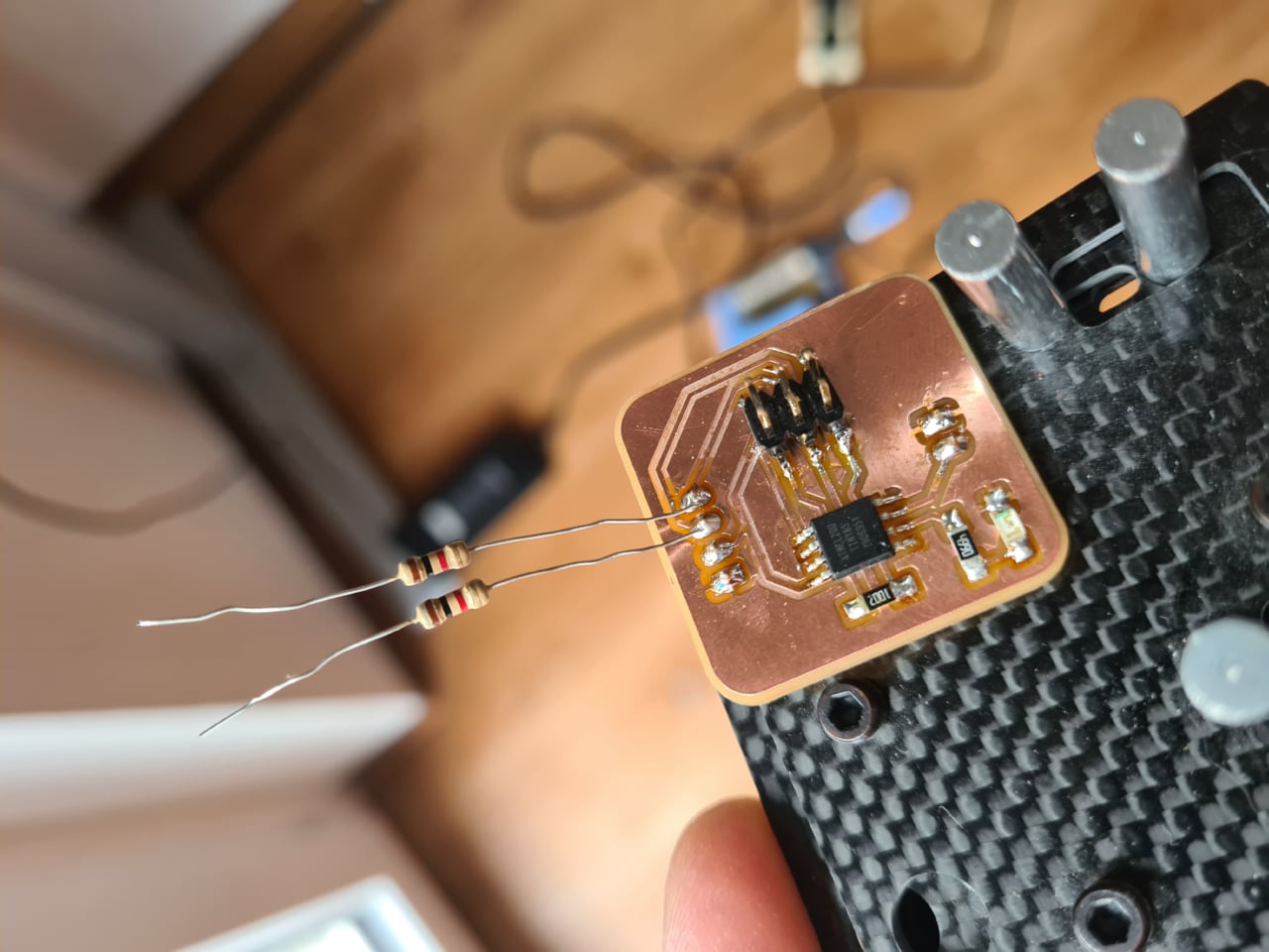
As part of the global review, I designed and made a little 30x30 mm board that ties into my final project using the I2C bus. The board uses a minimal ATtiny85 micro controller setup. The ATtiny85 is a very minimal microcontroller with only 8 pins, 2 of which are for VCC and GND, respectively. This leaves only 6 pins for general input/output (GPIO) purposes. I wanted to reserve the four ISP programming pins (MOSI, MISO, SCK, RESET, plus VCC and GND of course) for programming and communications functionality exclusively, so that left me with 2 GPIO pin to work with. Enough for an input and an output device. I decided to add an LED to the board as an output device and a button on a cable as an input device. Communication with the main project board would happen via I2C, tying this nicely into the networking topic. The two SDA and SCL pins needed for I2C communication were overlapping with the ISP pins, so there would not be any conflict with the remaining GPIO pins.
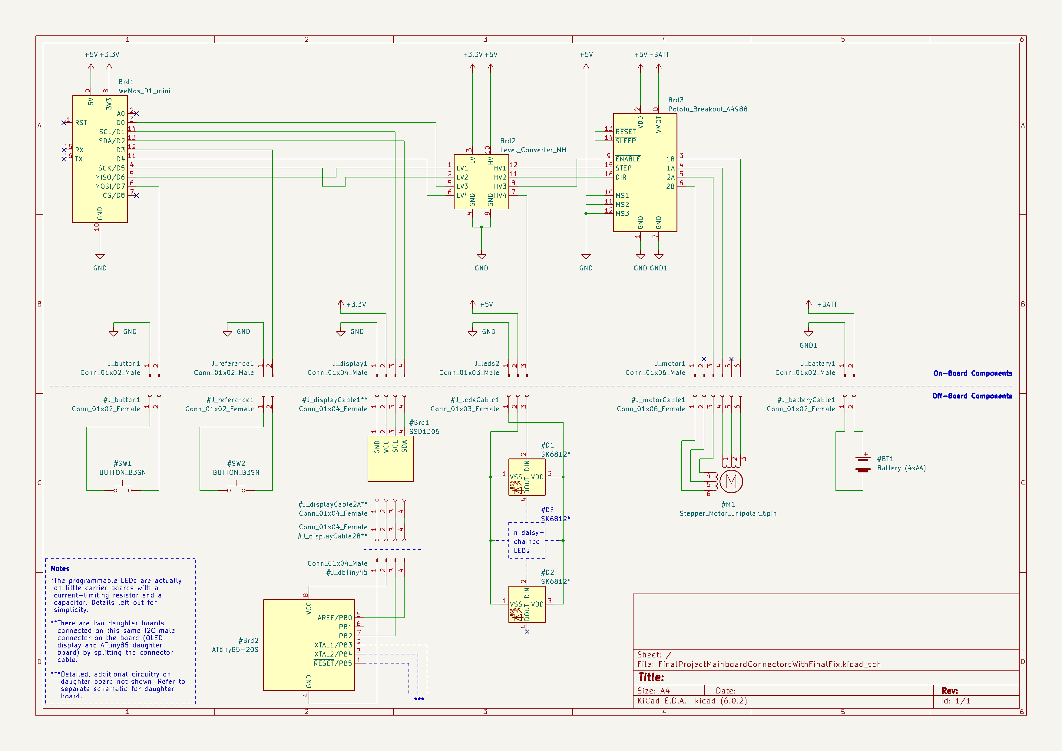
The I2C communication would look as follows: The main project board with the ESP8266 micro controller already uses the I2C bus for talking to an OLED extension board. The newly designed board would tie into the existing I2C bus connection (JST connector header) by means of a self-made Y-splitter cable. The ESP8266 board will continue to act as an I2C master node, whereas the new ATtiny85 board with button and LED will act as a slave/secondary on the bus. In the main node’s main loop, the ESP8266 master will poll the ATtiny85 secondary by sending a request on the I2C bus, requesting 1 byte of data. The secondary node will have a request event that, when triggered by the master, will read the button pin and return the state of the button as ‘0’ (not triggered) or ‘1’ (triggered). The master node will then act on this information by triggering the weather display, if the secondary node’s button is pressed. At the same time, the secondary node will start flashing the LED once noticing a button press on its side.
I started by designing and making the little extra board. I placed an ATtiny85 in the schematic, then added the 6-pin ISP header, a 4-pin I2C header, a 2-pin button cable header, a pullup resistor for the reset pin and an LED on pin PB3, along with its accompanying current limiting resistor. The button I placed again as a virtual component in KiCad, so it would be visible in the schematic, but be ignored when making the board layout. Here is both the daughter board schematic as well as the overall system schematic incorporating the new daughter board:
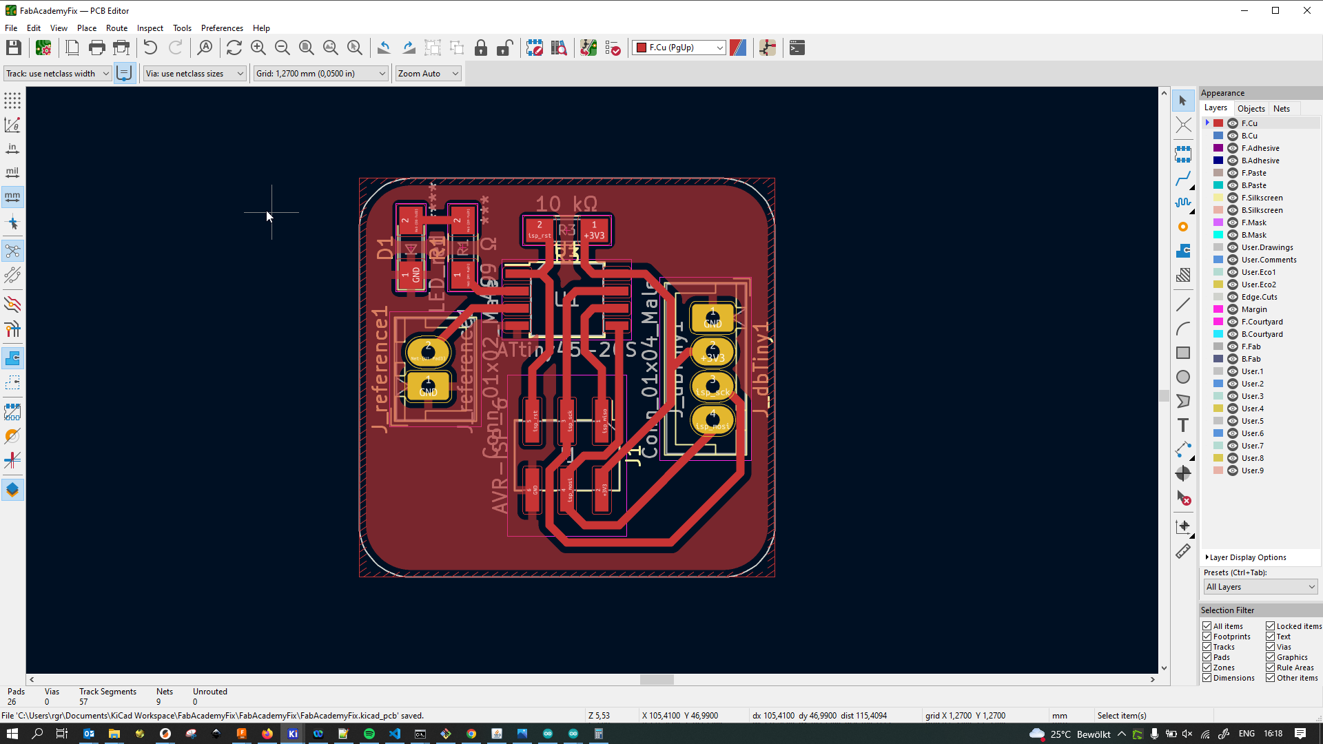
After putting down a ground fill and routing all the connections, I fattened up all traces to 0.6 mm and 0.2 mm clearance to avoid problems during routing the board. All holes for the through-hole header components were set to a hole size of 1 mm.
I then exported the file as an SVG (front copper, edge cuts and holes layers) and merged them into one file in Inkscape. I then added 5 mm padding on all sides to the file and exported the copper, edge cuts and hole pictures as 1500 dpi PNG files separately. I loaded up Mods in the browser and prepared the RML files for cutting on the Roland SRM20 using following parameters:
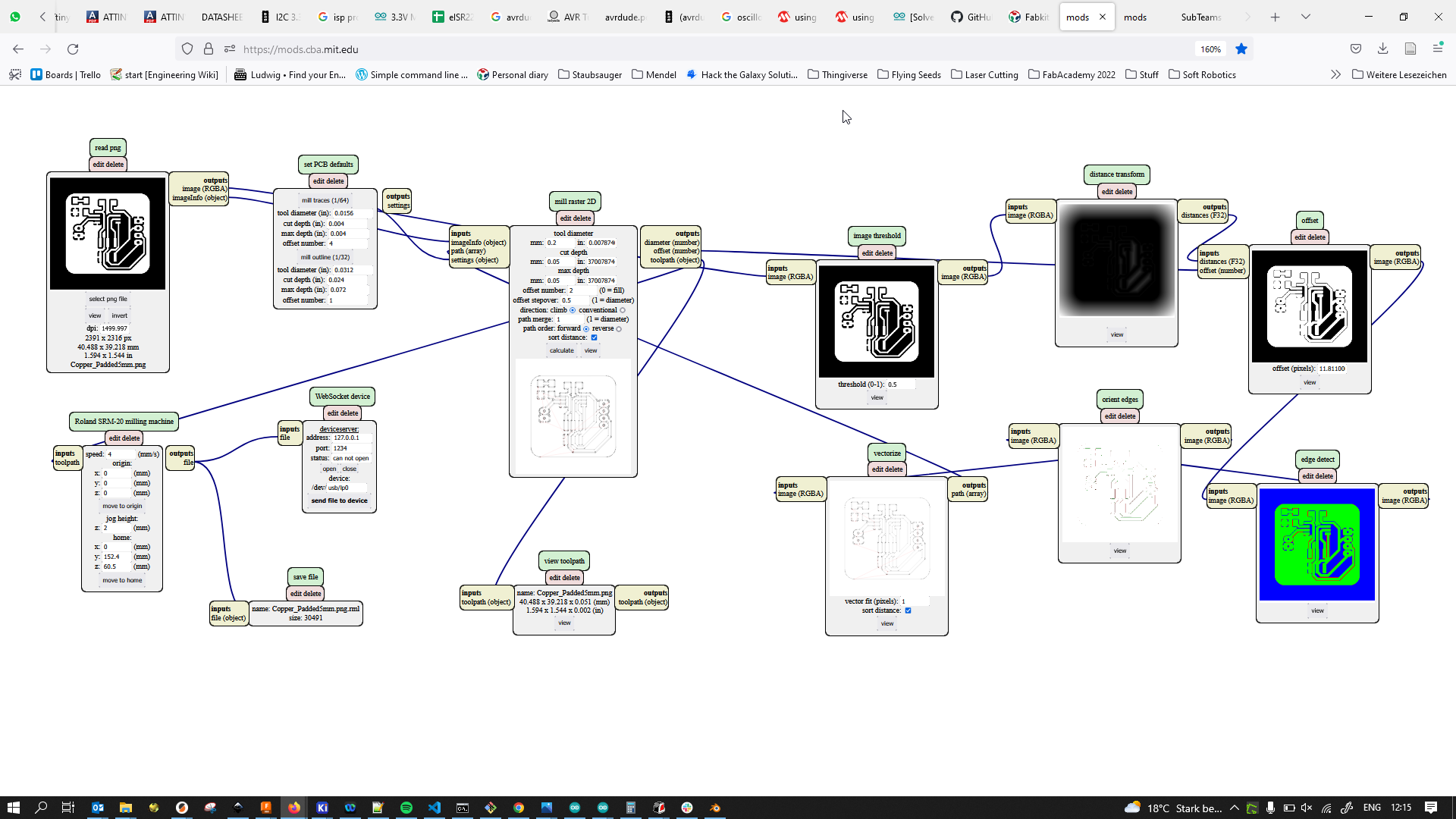
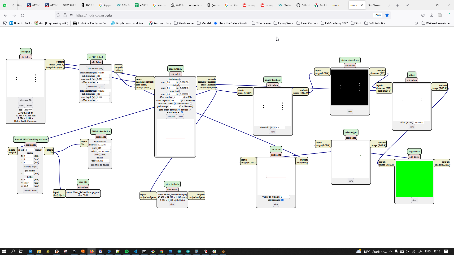
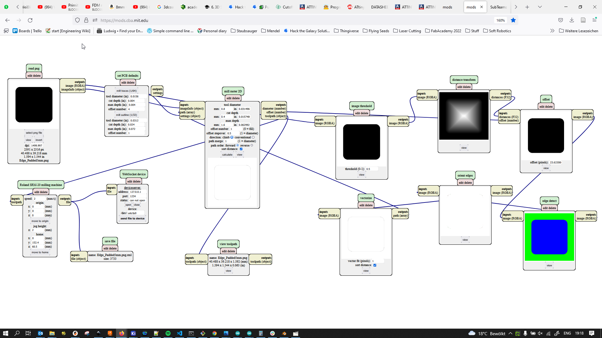
The copper traces I milled using a v-tip bit (labeled 0.20-0.50). The edge cuts and the holes were made using a 0.8 mm mill bit, so with the holes being 1 mm diameter, they could be milled with small spiraling, too. After cutting the board, I noticed I had accidentally left the option to print mirrored on in KiCad, meaning that my whole design was horizontally mirrored… D’uh! I repeated the whole process with a non-flipped version of the design. After cutting and removing the board, I gave it a quick polish with steel wool and cleaned it with water and detergent, followed by an alcohol wipe. I then added the ATtiny85 and all the other components, which went without problems.
Here is the daughter board starting to mill in the SRM20 …
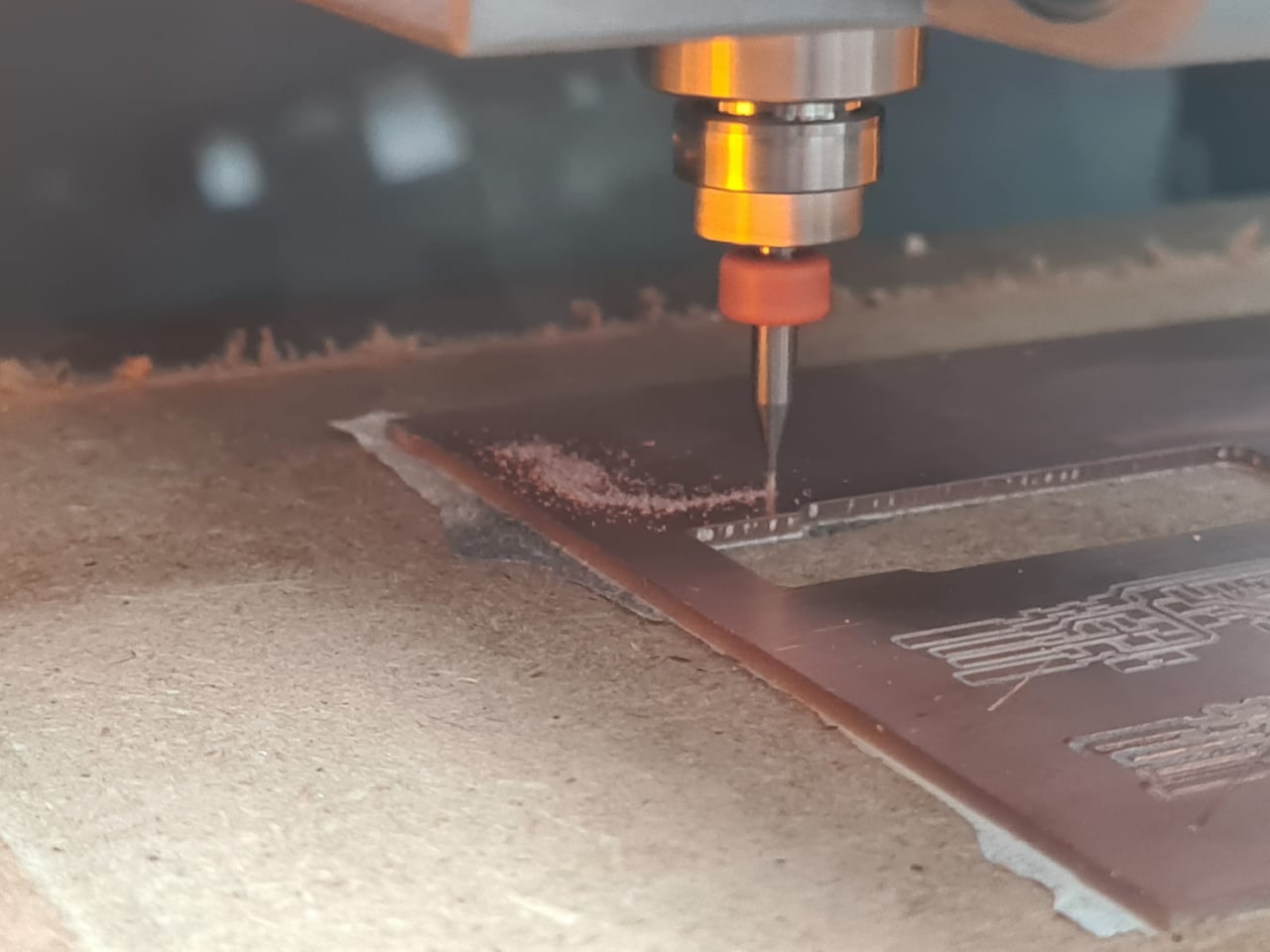
… and after drilling the holes for through hole components.
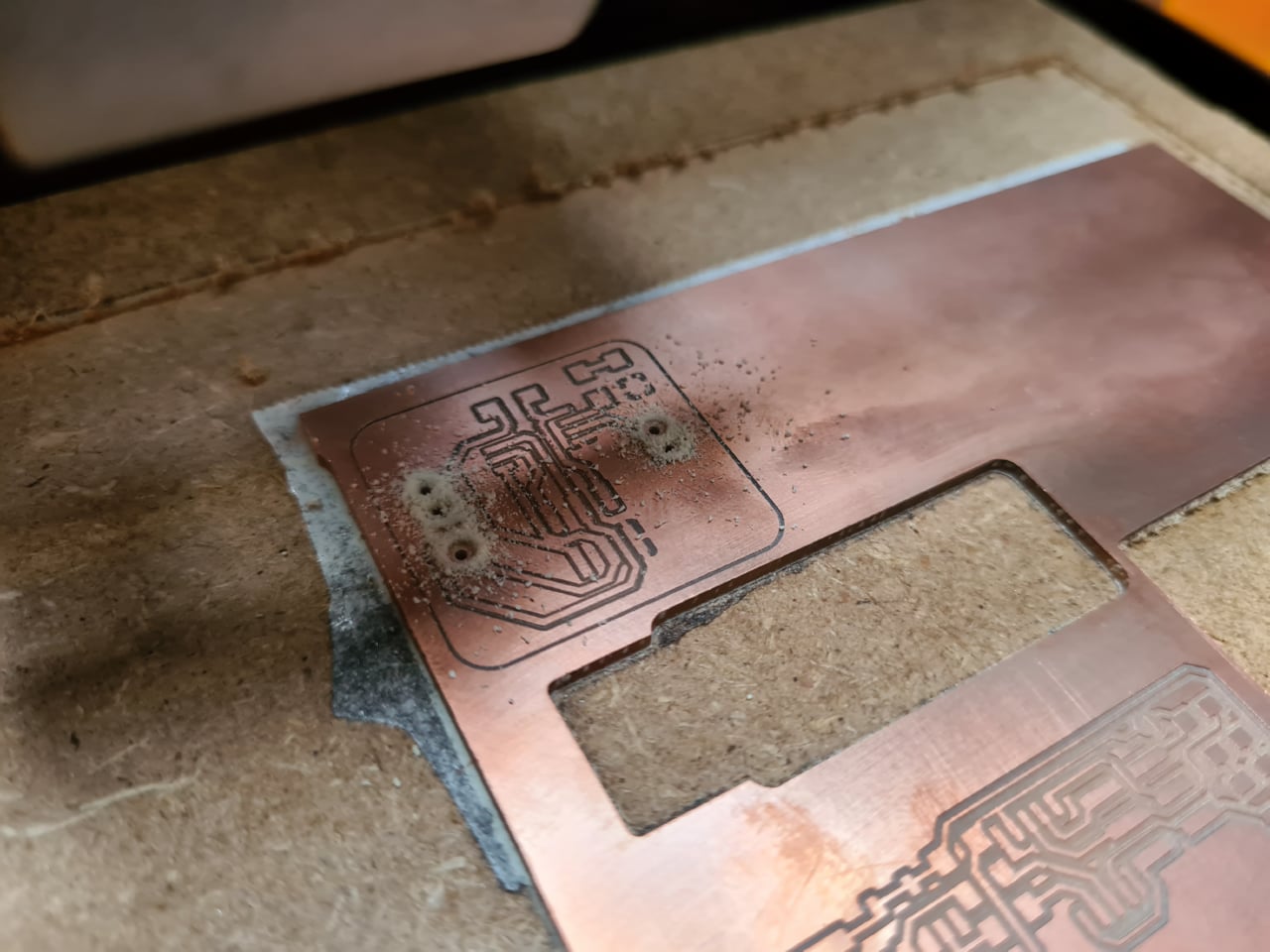
Here I noticed that the board was flipped and I had to remill it. D’uh!
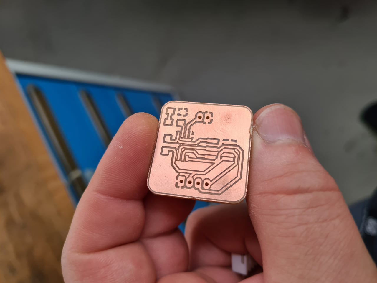
Here is the finished board top side …
… and the bottom side …
… and an isometric view showing both electronics and connectors:
After finishing up the board, I tried to upload the Blink sketch onto the board using the Arduino IDE, using my self-built USBtinyISP. Preparations for working with the ATtiny25/45/85 in Arduino IDE had already been made in a previous week when installing the ATtiny core in Arduino IDE to work with an ATTiny44, so I did not have to prepare anything there besides selecting the proper ATtiny85 chip. Unfortunately, the sketch would simply not upload. Upon closer inspection, I noticed that there was a little copper bridge halfway underneath the 6-pin ISP header tying the MOSI pin to 3.3V and thus preventing communication.
After stuffing and soldering the board, the board simply would’t upload with my USBtinyISP:
I severed the connection with a box knife and checked for continuity with a multimeter. When the connection was severed, I tried uploading again and it worked!
For the Blink sketch I had to use pin 3 as LED pin, as the LED was connected to PB3 on the ATTiny and that translates to 3 in Arduino terms. I used following cheat sheet for all following checks for which pin numbers to use:
//picture of ATTiny cheatsheet
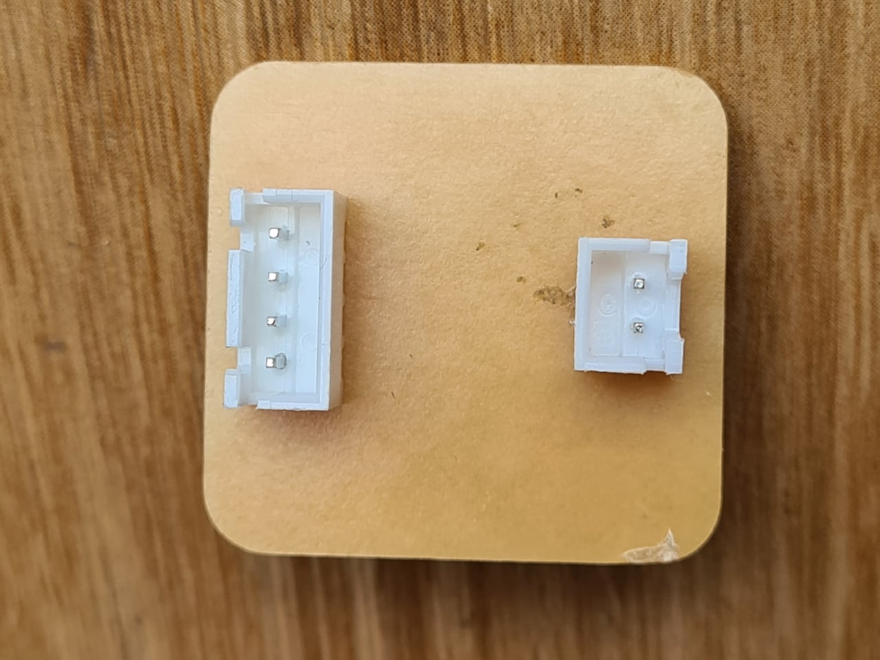
After making sure that the LED worked, I also prepared the button by soldering a microswitch to a 2-wire cable and crimped a JST connector to the other side. This button would connect to the 2-pin JST header on the daughter board. For the I2C connection, since there only was one I2C header on the ESP8266 main board and it was already occupied by the OLED screen connection, I cut the 4-wire cable connecting the main board to the OLED screen in half and crimped another 4-pin JST connector in between, making it a Y-splitter cable. I then noticed that I had soldered the 4-pin JST header (which are keyed to prevent reversed polarity) onto my daughter board the wrong way around. Instead of trying to desolder the 4-pin connector at home with my crappy soldering iron, I decided to simply pop out the contacts out of the JST connector and revert the 4 wires in the connector, so even with the keying the correct wires were connected to the correct pins.
Here is the I2C cable split in half to accommodate both the OLED screen connection as well as the daughter board …
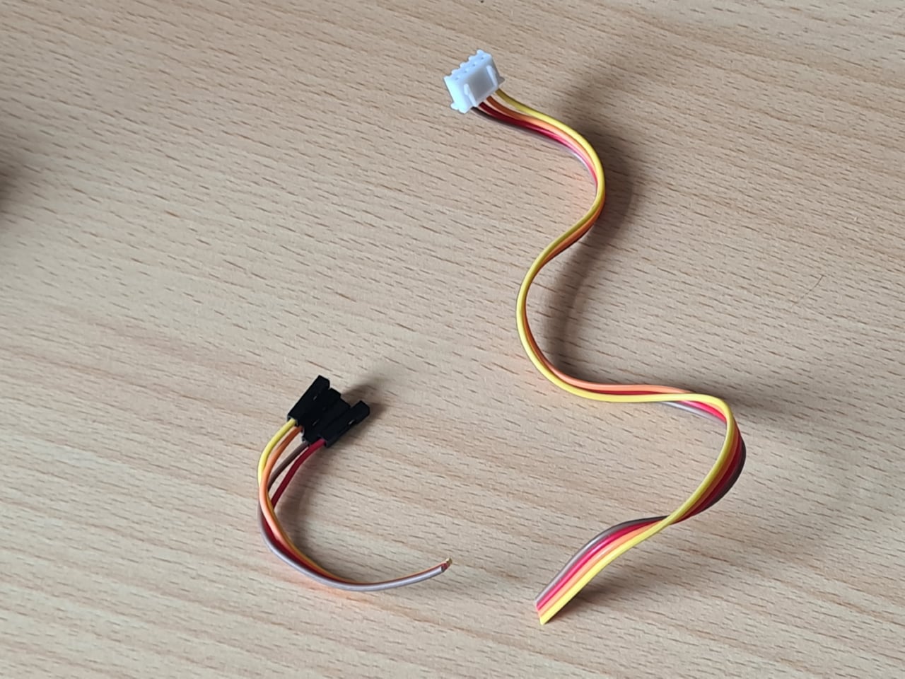
… and the resulting Y-split cable:
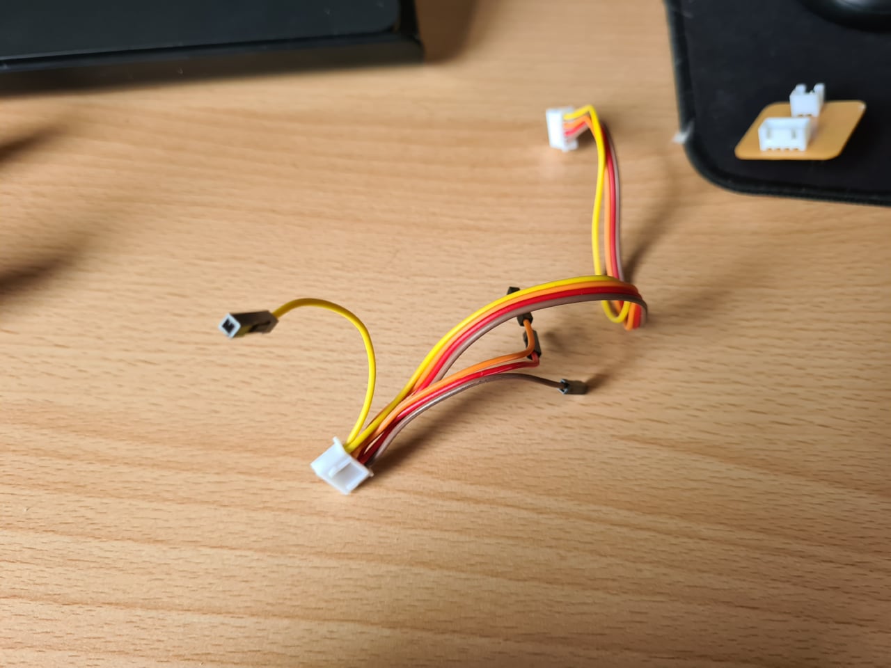
Here is the ATtiny85 daughter board connected into the common I2C bus of the final project device:
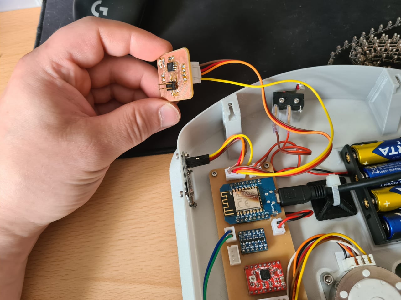
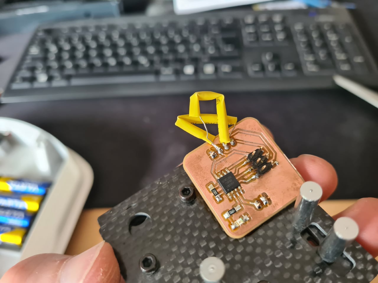
After connecting the board, I noticed I had forgotten the pullup resistors on the I2C bus. I added 1k resistors to both data and clock lines of the I2C bus …
… and insulated them using heat shrink tubing:
I then went ahead and implemented the program for the daughter board and changed the main board program to also take the daughter board into account. This was a little more futzing around than I care to admit, but in the end I arrived at a working solution.
Some test code to see whether the data transfer between I2C secondary node and master node works:
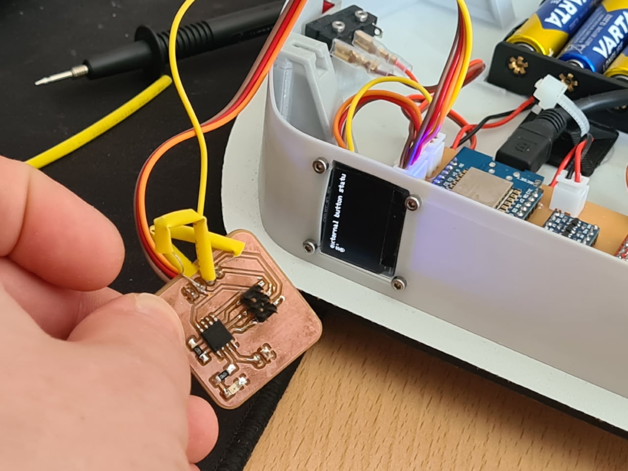
On the daughter board, inside the main loop the board constantly polls the attached button. If the button is pressed (and thus pulled to GND), the board notes this change, turn on its LED to indicate it registered the button press and stops polling the button. At the same time, the main board regularly polls the secondary board via I2C by sending I2C requests, using the Wire library. It only requests one single byte of data from the daughter board. The daughter board upon those requests returns whether the button had been triggered in the meantime and resets its state. If the daughter board returns that a button press event had happened, the main code starts the weather forecast display process, the same as when pushing the internally connected button.
Here is a little demo video of the daughter board tied into the final project device:
This way, the external button can be placed somewhere apart from the device, maybe inside a plush toy or sth else the children might interact with. This is something to tangibly implement in the future though, but the provisions exist.
Design Files
- Network #1 Codes (INO, Arduino IDE)
- Network #2 Codes (INO, Arduino IDE)
- Addendum Master code (ESP8266 Arduino Code) (INO, Arduino IDE)
- Addendum Secondary code (ATtiny85 daughter board Arduino Code) (INO, Arduino IDE)
- Addendum ATtiny85 daughter board design files (KICAD_PRO/KICAD_SCH/KICAD_PCB, KiCad 6.0)