7. Electronics design
Group Work
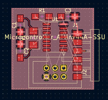
A detailed documentation of our group assignment work can be found on the shared group assignment webpage.
Background - Electronics Design
When I got into Electronics around 2009ish, I pretty quickly started making my own circuit board designs using EAGLE. I mainly worked on LED designs, like a POV-wand with LEDs or a Word Clock with LED matrix. The boards were designed for being toner-transferred and then etched, not milled. In the years following, I only worked on electronics design intermittently, using EAGLE and later Fusion360 (when they implemented that functionality). I hadn’t used KiCad until FabAcademy.
Designing a Board
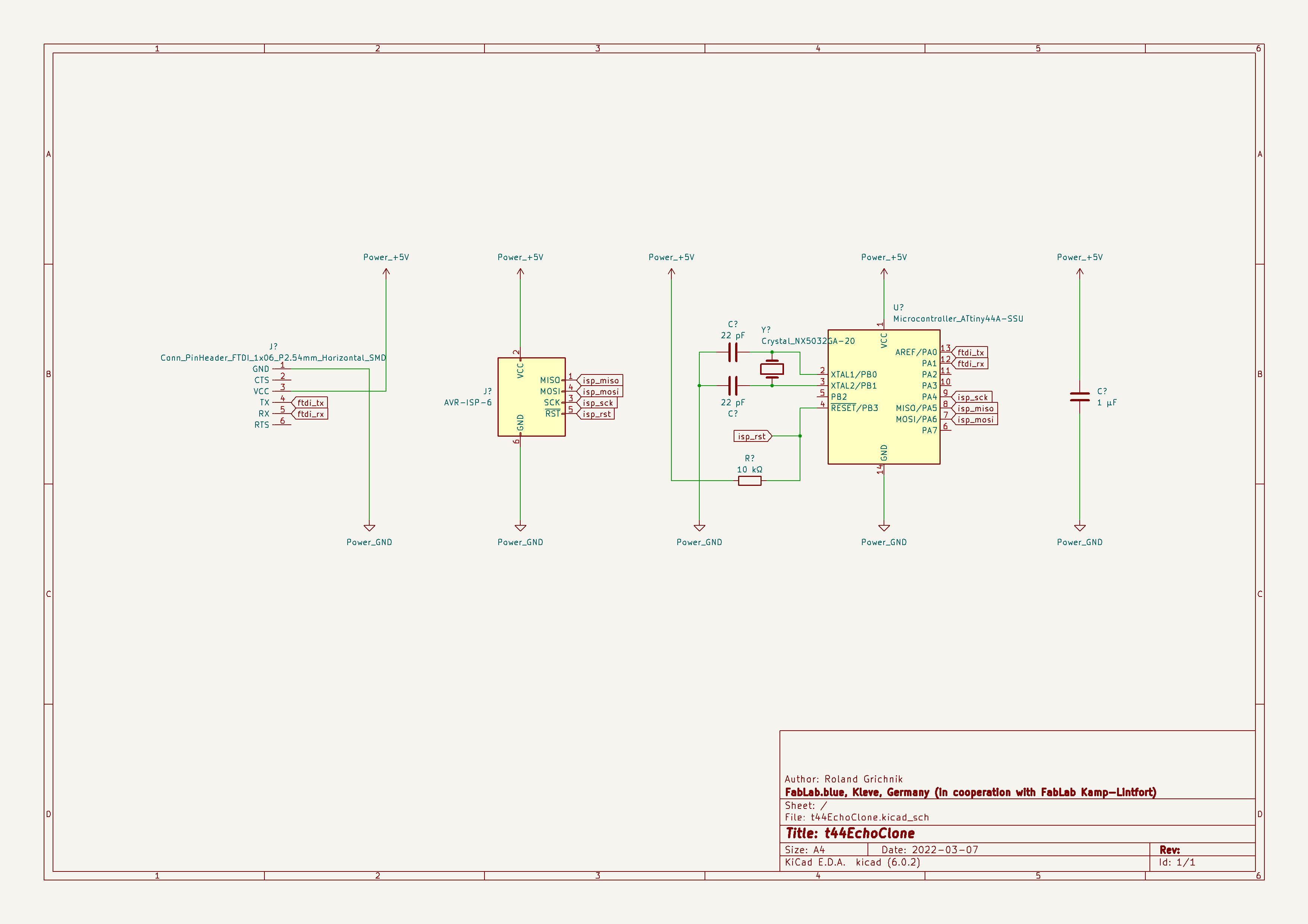
For this week’s assignment, we were tasked to “redraw an echo hello-world board, add (at least) a button and LED (with current-limiting resistor)[,] check the design rules, make it, and test that it can communicate”. Since we had ATTiny44 microprocessors available at the moment of starting the design, I decided to use the ATtiny44 version of the echo board as a starting point.
Preparing KiCad
- Install KiCad 6.0
- In preparation, we downloaded and installed the Fab libraries for both symbols and footprints for KiCad
Starting a new project
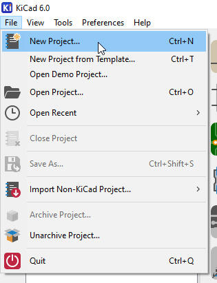
I started out by adding a new project in KiCad…
…making a new folder for it…
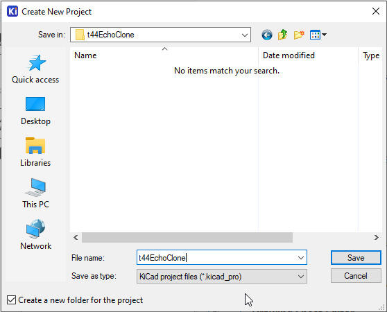
…and calling it t44EchoClone - given that it was a clone of the t44Echo board, I guess that fit well. :)
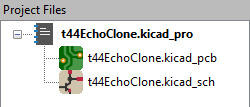
The new project (.kicad_pro file) contains (or rather links to) both a schematic (.kicad_sch) as well as a PCB design (.kicad_pcb file):
After creating the project and opening up the schematic file, a blank schematic comes up (as an A$ page of paper to start out with):
![]()
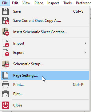
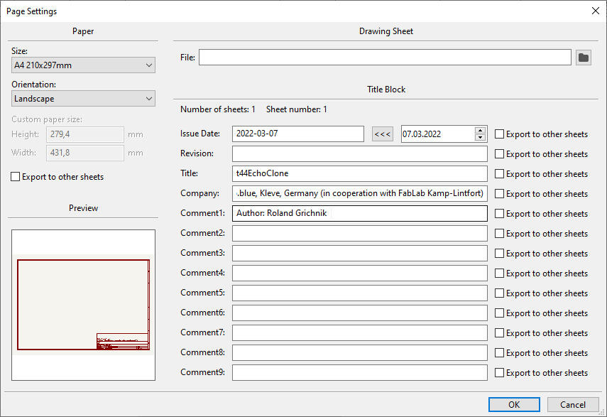
First, I went into the Page Settings to change the contents of the lower right text field by going to File -> Page Settings…
…and changing the Issue Date, Title and Company as well as adding more information:
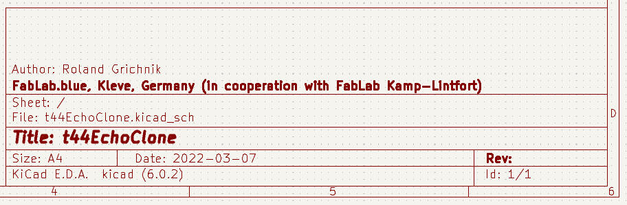
The added information automatically gets added to the bottom right text field in the schematic page:
Adding symbols
The blank page is now to be filled with the electronic circuit schematic that we want to produce in the end. Before making the actual PCB and routing connections on the PCB, we create our logical circuit in the schematic only.
To that end, we start by adding components to our schematic. These symbolic representations of the components, which don’t necessarily reflect the physical component, are called “symbols” in KiCad. Adding symbols can be done from the right tool bar or by pressing A:

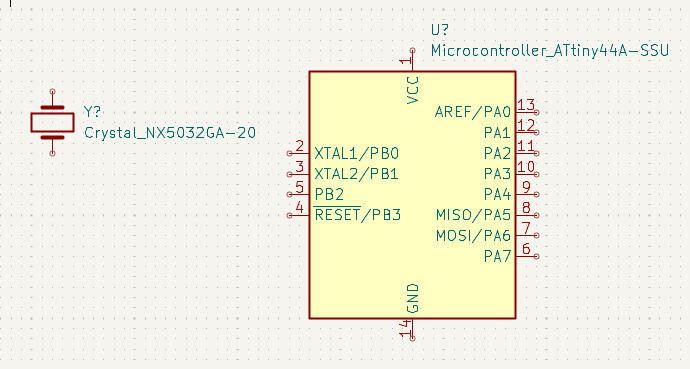
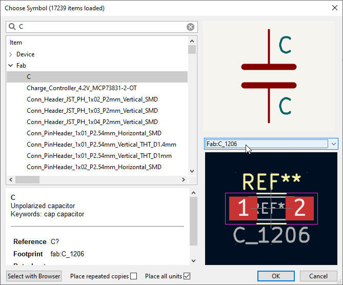
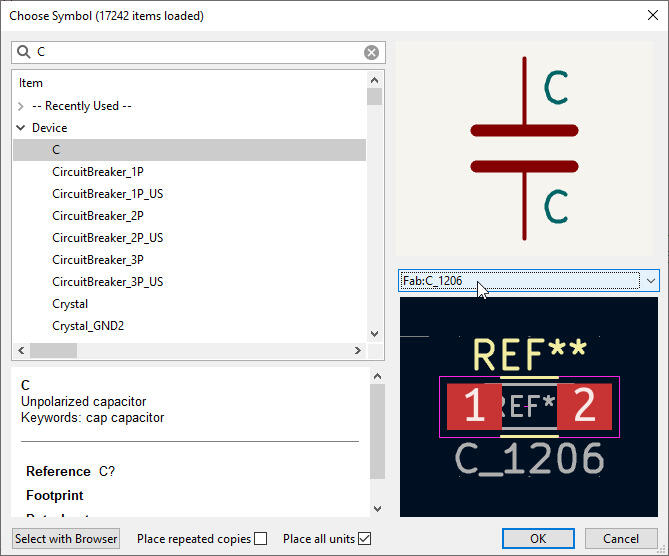
When adding symbols, a popup window comes up which has a search bar for searching component symbols. I wanted to start with the microcontroller as the center piece, so I searched for ATTiny in the search bar. This filters the list of components. I then picked the ATtiny44 component from the Fab library:
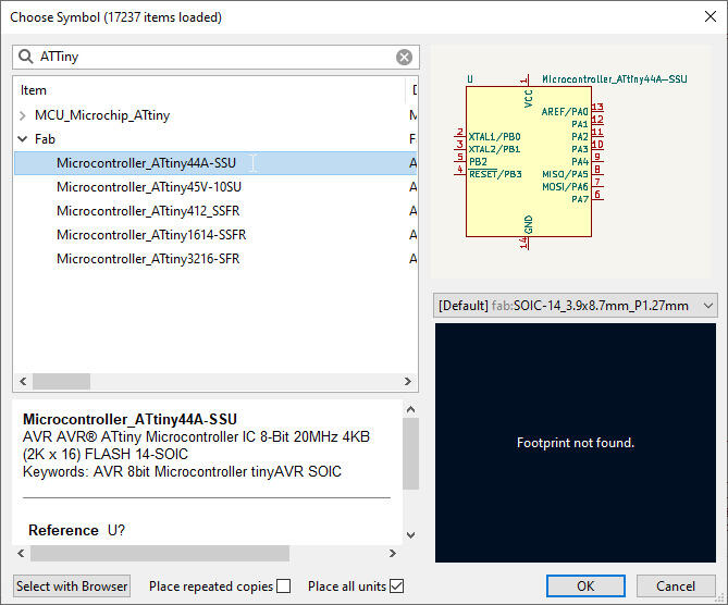
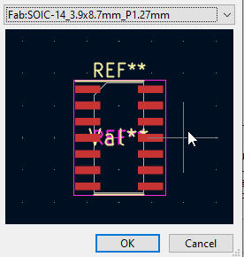
As can be seen on the previous picture, it says “Footprint not found”. This means that the chosen symbol does not have a footprint assigned to it. Footprints are the shapes we need to place on our PCB later to attach the physical components to. This can be fixed directly by extending the drop down menu at the bottom right and selecting the fitting footprint preceded by Fab (meaning it comes from the Fab library)…
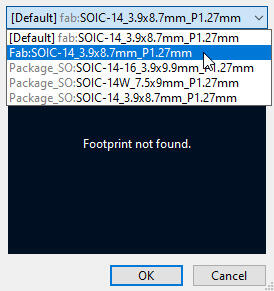
…which immediately shows the footprint chosen (in this case, a 14-pin SMD chip footprint):
After pressing OK, the symbol appears in the schematic and can be placed by clicking LMB:
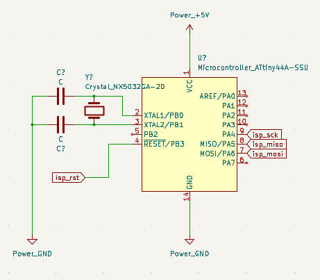
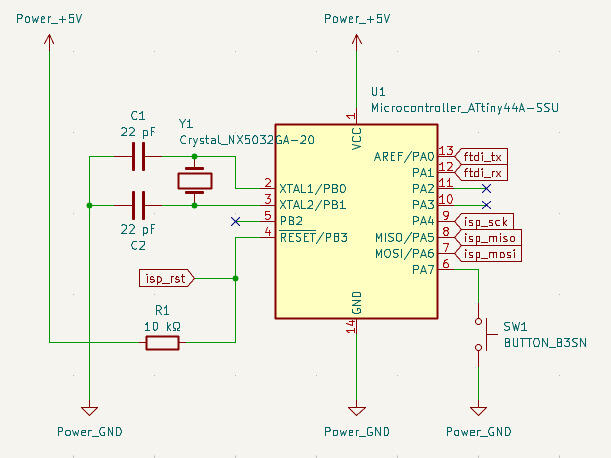
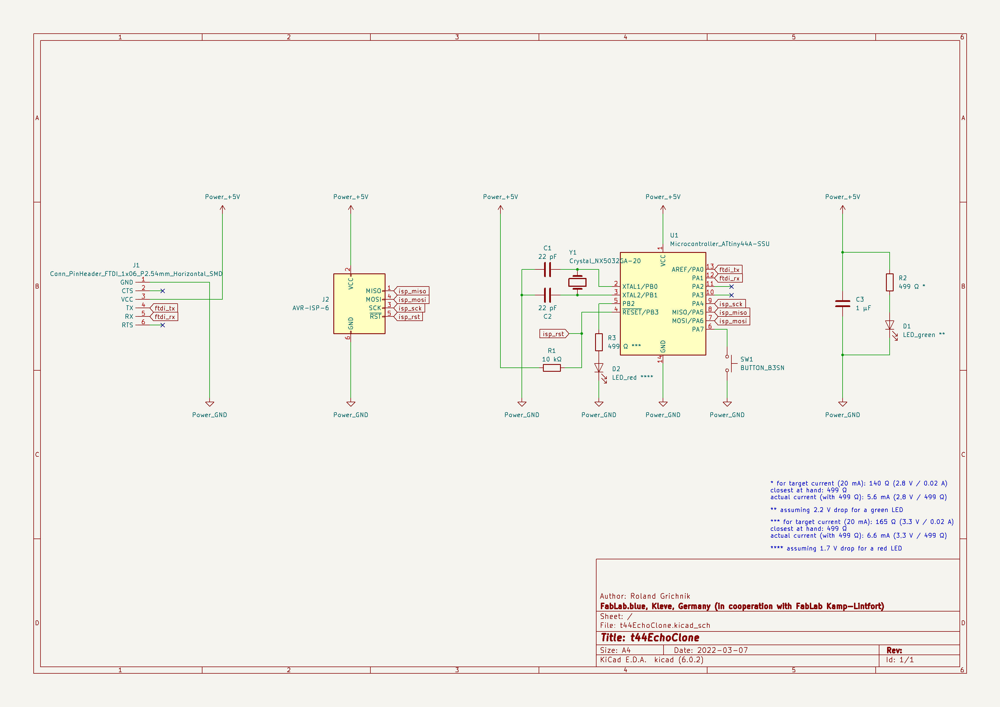
This is the board by Prof. Gershenfeld I wanted to redraw: The t44-echo using an ATtiny44:
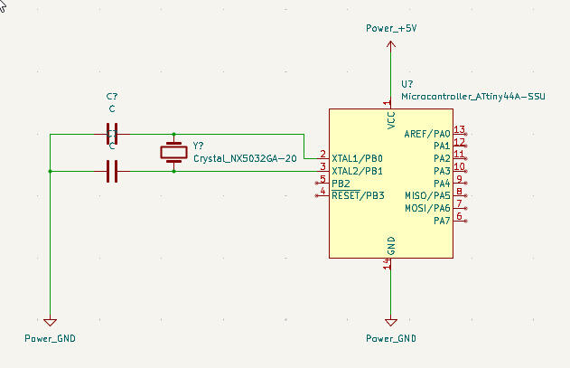
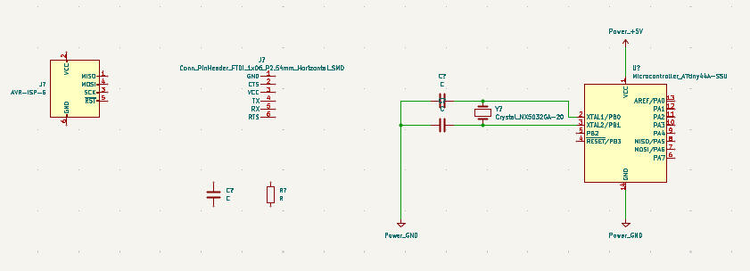
THe original design uses a resonator, whereas I decided to use a quartz and two capacitors due to availability. I started by adding the crystal…
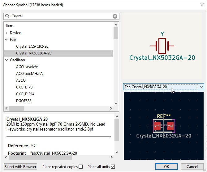
…placing it close to the pins marked XTAL in the schematic. These pins on the ATtiny44 (pins 2 and 3) are the pins for connecting an external clock source, like a crystal (see ATTiny44 datasheet page 25, 7.4 - Crystal Oscillator):
I then selected the wiring tool (hotkey W) from the toolbar and connected the pins (the little circular terminals) of the quartz to the XTAL pins by first clicking one end, then the other:

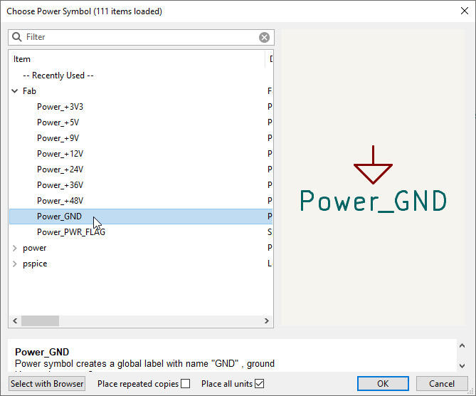
Afterwards, I added power symbols using the respective function from the toolbar (hotkey P):

I added one symbol for ground (GND)…
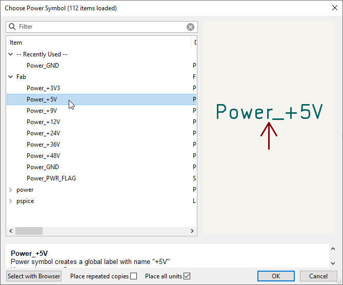
…and one for 5V, as 5 volt is my supply voltage:
I then also added two capacitors…
…connecting the terminals of the quartz to ground, by wiring them up with the GND power symbol in the schematic. Note that all GND connections are internally connected, so it does not matter which one it is connected to in the schematic. In my case, I actually added another GND symbol, so there wouldn’t be as much wiring to follow. Do whatever makes the schematic easy to read, not what exactly replicates the physical layout. It’s just a schematic after all, showing logical, not real-world, connections between parts:
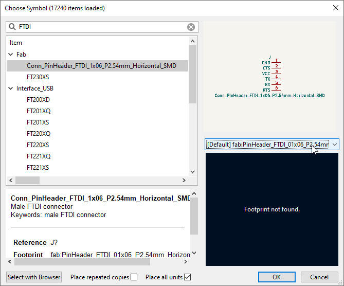
I then added the headers for the FTDI connector…
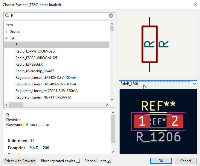
…as well as a resistor…
…and a capacitor…
…into the schematic, ending up with following:
To not mess around with too many wires (which would make the schematic hard to read), I added labels to the schematic…

to connect different pins on MOSI, MISO etc.:
Here’s what the 6-pin ISP header looks like with all pins wired up, but nor directly to something else in the schematic, but just to labels (here: isp_miso,isp_mosi,isp_sck and isp_rst):
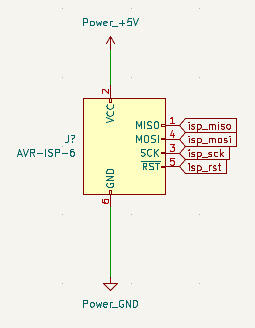
The pins on the microcontroller that would need connecting to the ISP header were connected to labels of the same name, telling KiCad that all these pins (on the respective identical label) would be connected:
I did similarly with ftdi_tx and ftdi_rx to wire up the RX and TX pins from the FTDI connector…
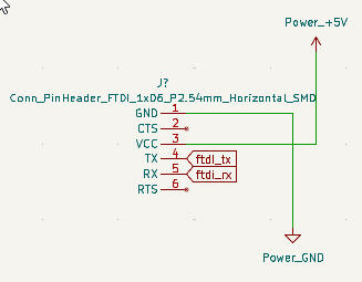
…and then, again, added connections to these same labels on the micro controller part:
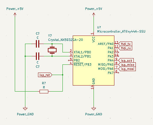
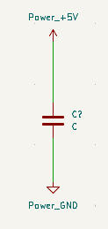
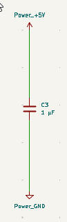
I also added a smoothing capacitor between 5V and GND, explicitly placed on its own in the schematic to emphasize its singular function:
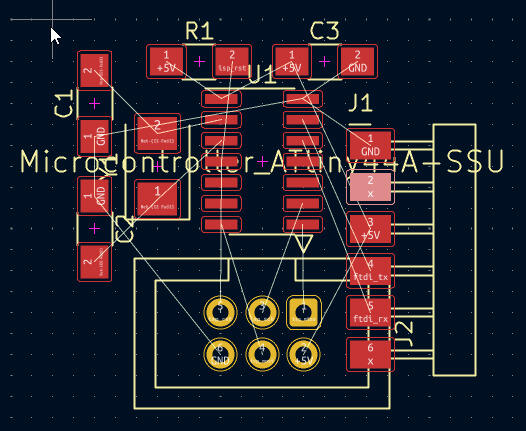
Here’s an overview of where I was at that point so far:
To make the transition to a PCB design, I ran the function to Fill in schematic symbol reference designators…
![]()
…which numbers parts yet unnumbered automatically:
![]()
A few footprints still had to be assigned now, which could be done by clicking Run footprint assignment tool…
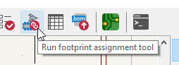
…and then assigning proper footprints manually in there:
Finally, by pressing Open PCB in board editor, a PCB design could be started from the schematic at hand:
Going Physical - Schematic to Circuit Board
Since I had generated the PCB Design file at an earlier time already, initially it started out blank for me:
![]()
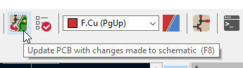
By running Update PCB with changes made to schematic, all the changes made to the schematic can be transferred (selectively, if wanted) to the PCB design:
Immediately, the footprints for my parts popped in:
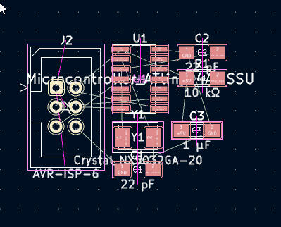
I started out by laying out the parts so that the ratsnest wires (the yellow, thin lines in the picture), which show logical, yet not yet routed connections, would show as little overlap as possible - there is a big part of feel and intuition involved here:
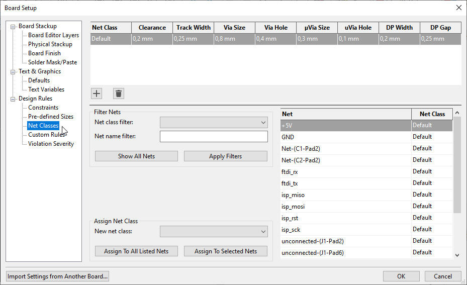
I then went into the Board Setup…
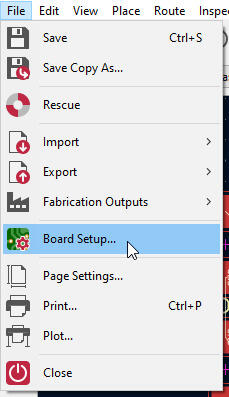
..and set up the general, standard values for my net classes (to set default trace widths and clearances):
SInce I wanted a copper ground plane, I clicked the icon Add a filled zone…
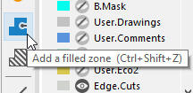
…and had it connect to GND:
I then used the tool to draw the filled zone outline on my PCB…
…and used button B to fill the zone (this button needs to be pressed anytime the zone should be updated, e.g. when a new connection was routed):
The copper ground plane is connected to GND pins using thermal reliefs (the cross shaped traces connecting them to the pads) to allow easy soldering - if the GND pad was just part of the big ground fill, without any gaps, it would solder very badly due to the huge copper mass wicking away all the heat quickly:
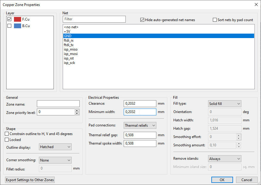
The final PCB design with copper ground fill looked as follows…
…and was neatened up slightly by adding rounded corners:
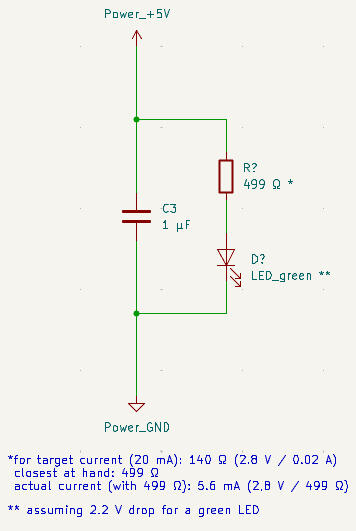
Back in the schematic editor, I wanted to add a power LED. Since the smoothing cap was - functionally - the part of the schematic dealing with power supply so far, I added to it…
by adding an LED and a current limiting resistor…
…into its functional block of the schematic:
I then also added and placed the footprint of a push button and an LED with resistor, without them actually yet being connected. I chose to put all three on the lower left corner of my board…

…and afterwards checked which pins of the ATTiny44 were actually situated closest to them - in this case pins PA7 and PB2 were the closest, so far unused pins:
I connected the push button in the schematic to PA7…
…and the LED with its current limiting resistor to pin PB2:
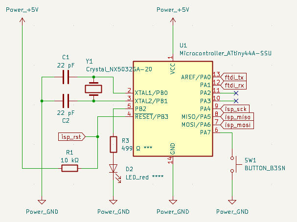
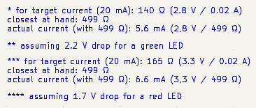
I then also added some descriptive text to show my design intent and why I chose certain resistor values:
File Export
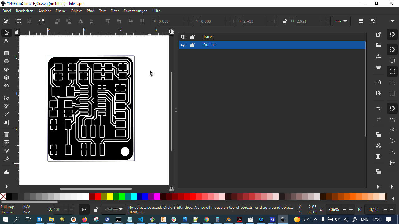
I then exported the final PCB Design file by clicking File -> Export -> SVG in the KiCad PCB Editor. I included the bottom copper, silk screen and edge cuts layers in my SVG export.
Fabricating the Board
File Prep
Both outline…
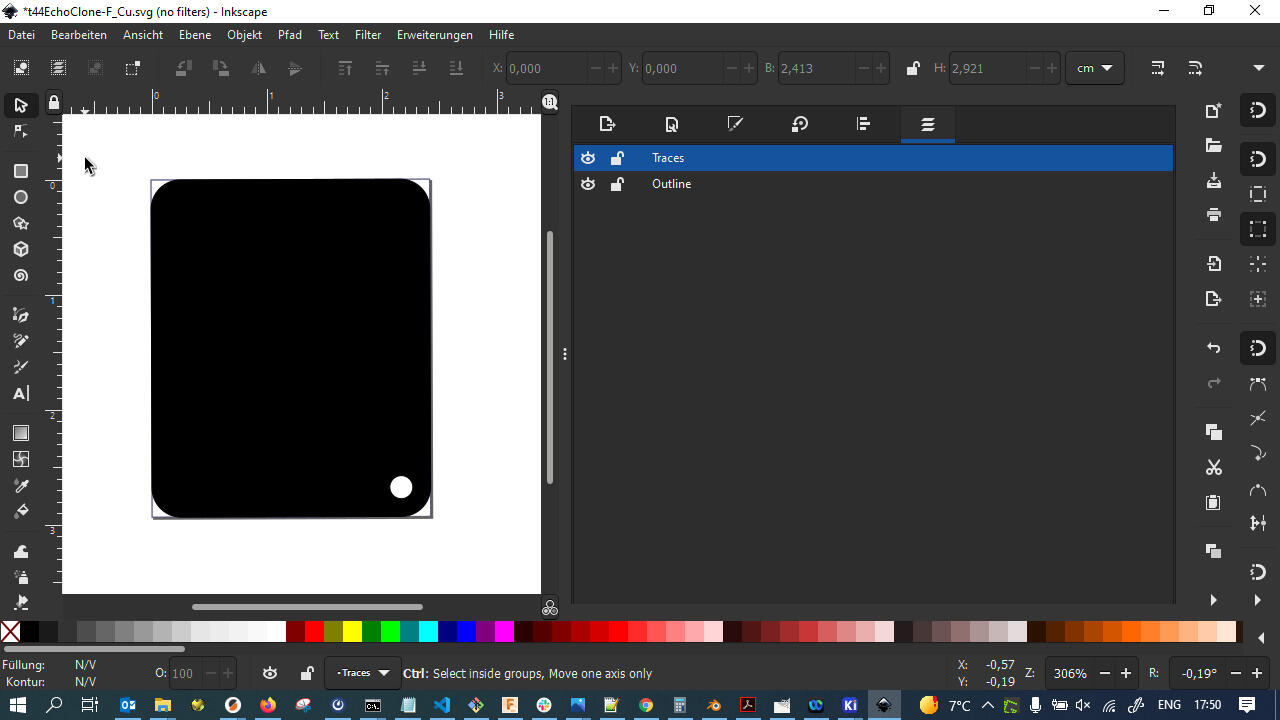
…as well as traces of the board were exported from Inkscape as a PNG raster graphic at a resolution of 1500 dpi:
Milling
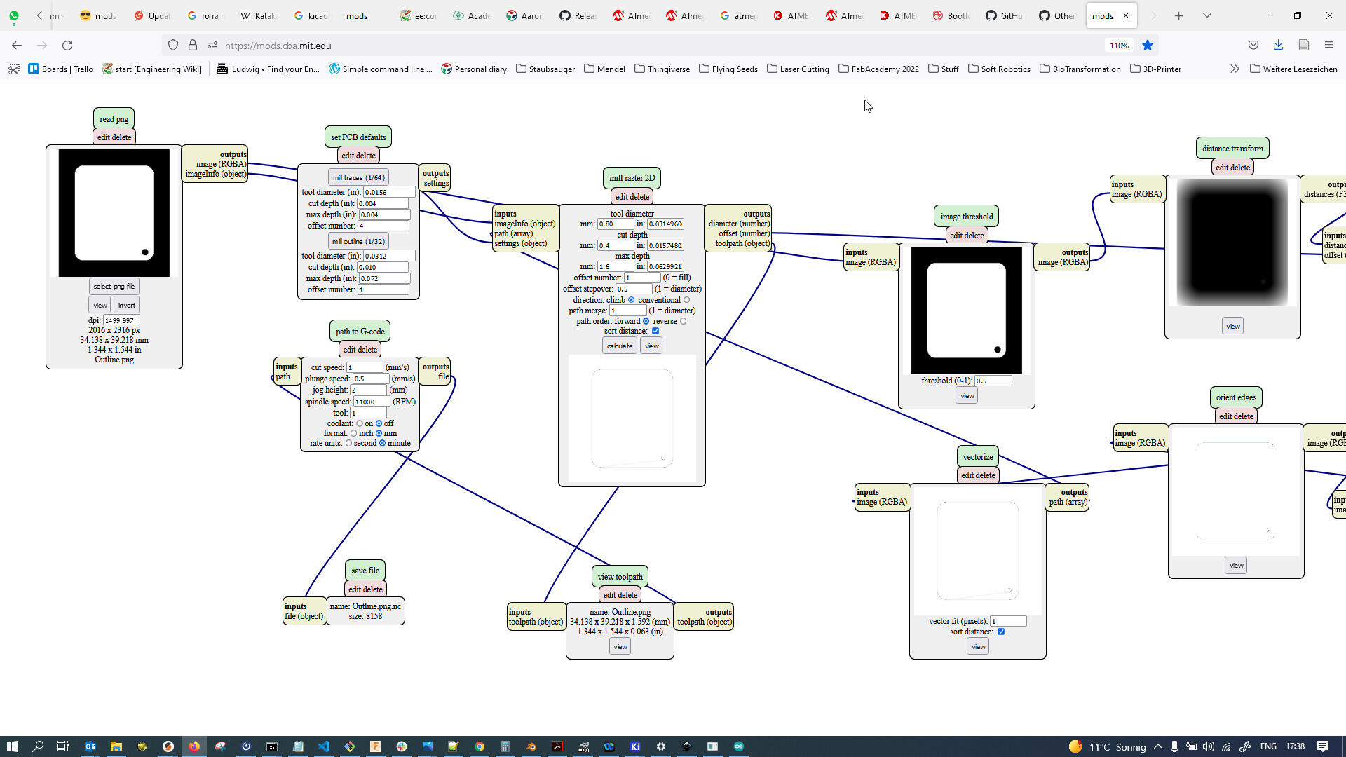
The resultant PNG file with the picture of the traces…
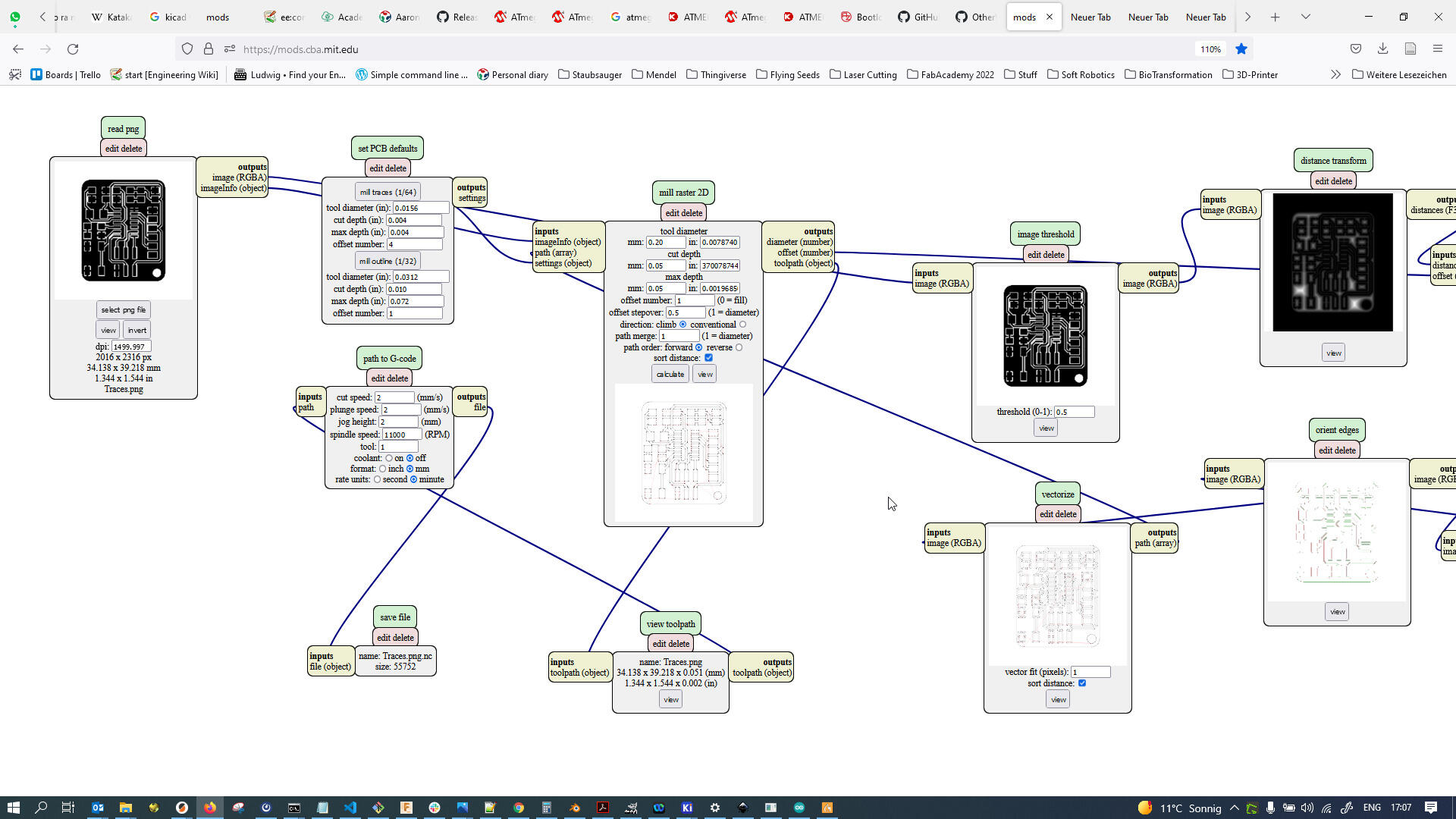
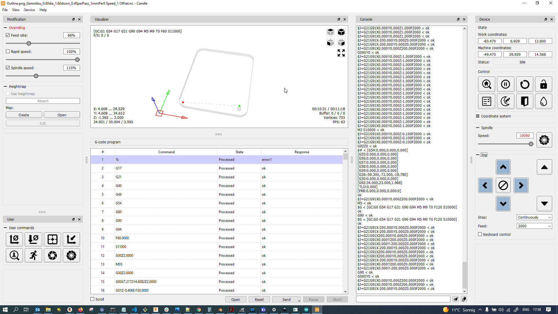
…as well as the outline was then opened with Mods and turned into GCode for the Genmitsu PCB Mill:
Both traces and outline (showing outline cut preview here only) were milled from single-sided PCB stock using Candle for GCode streaming:
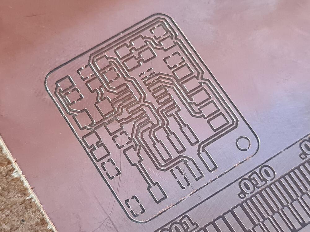
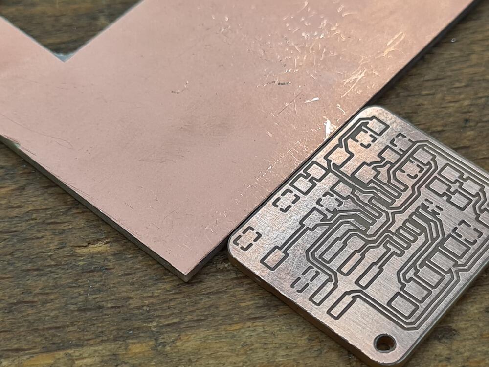
Here is the result after milling the traces:
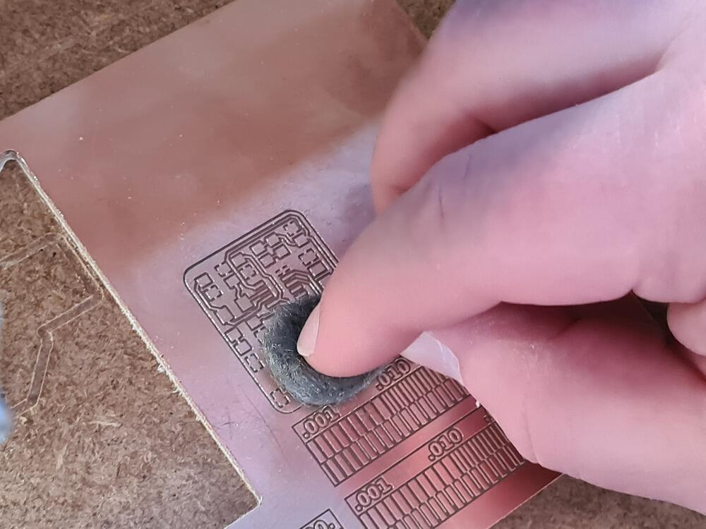
I then buffed the traces with steel wool to make the copper nice and shiny again…
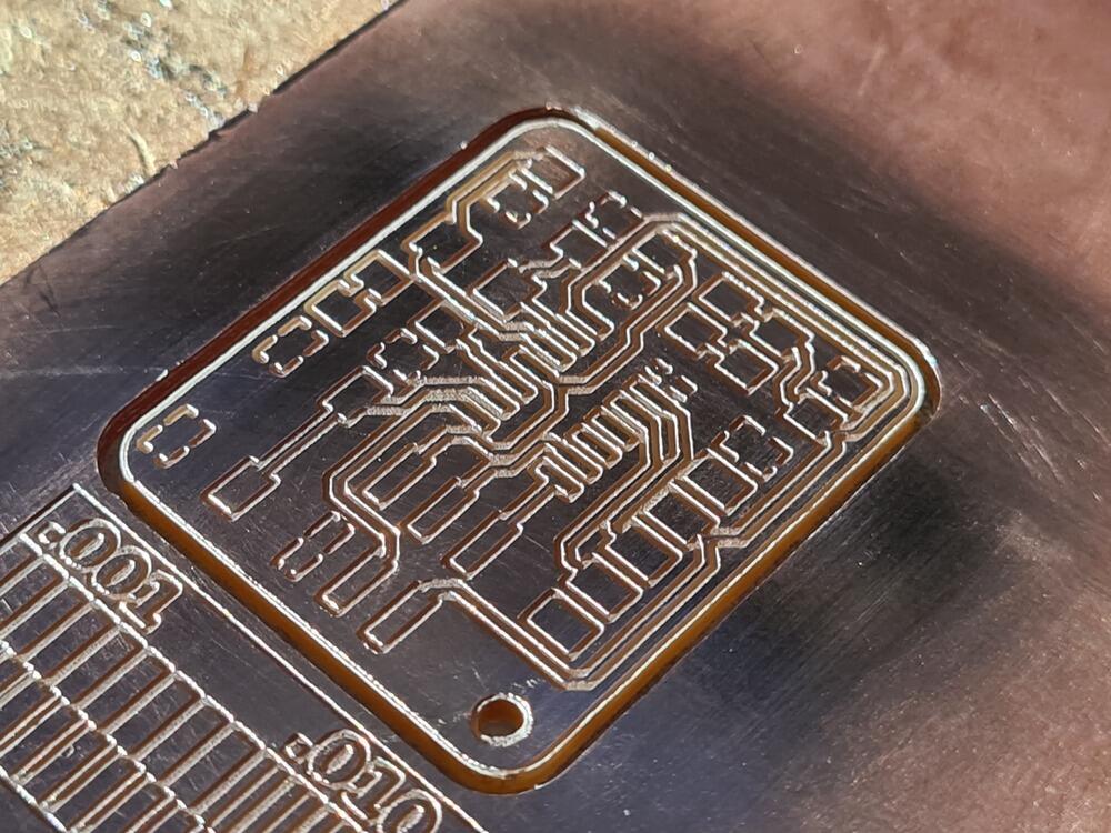
…and then cut the outline:
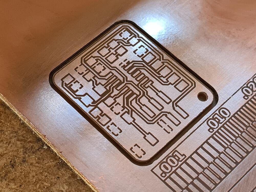
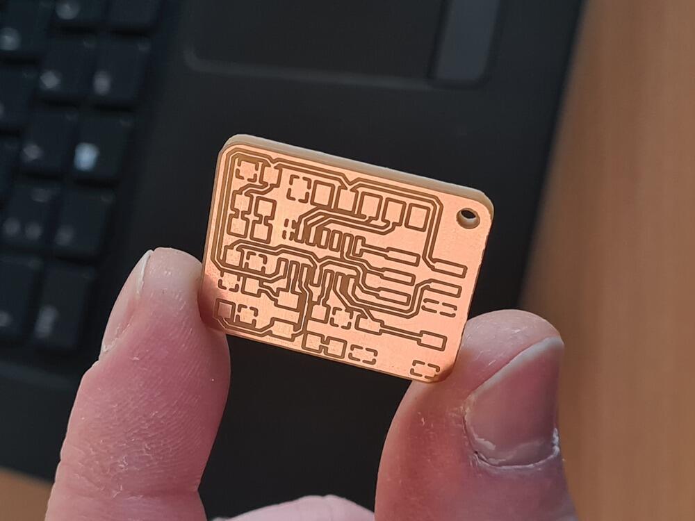
Here is the final board, buffed and with outline cut, ready for removal…
…and out of the machine:
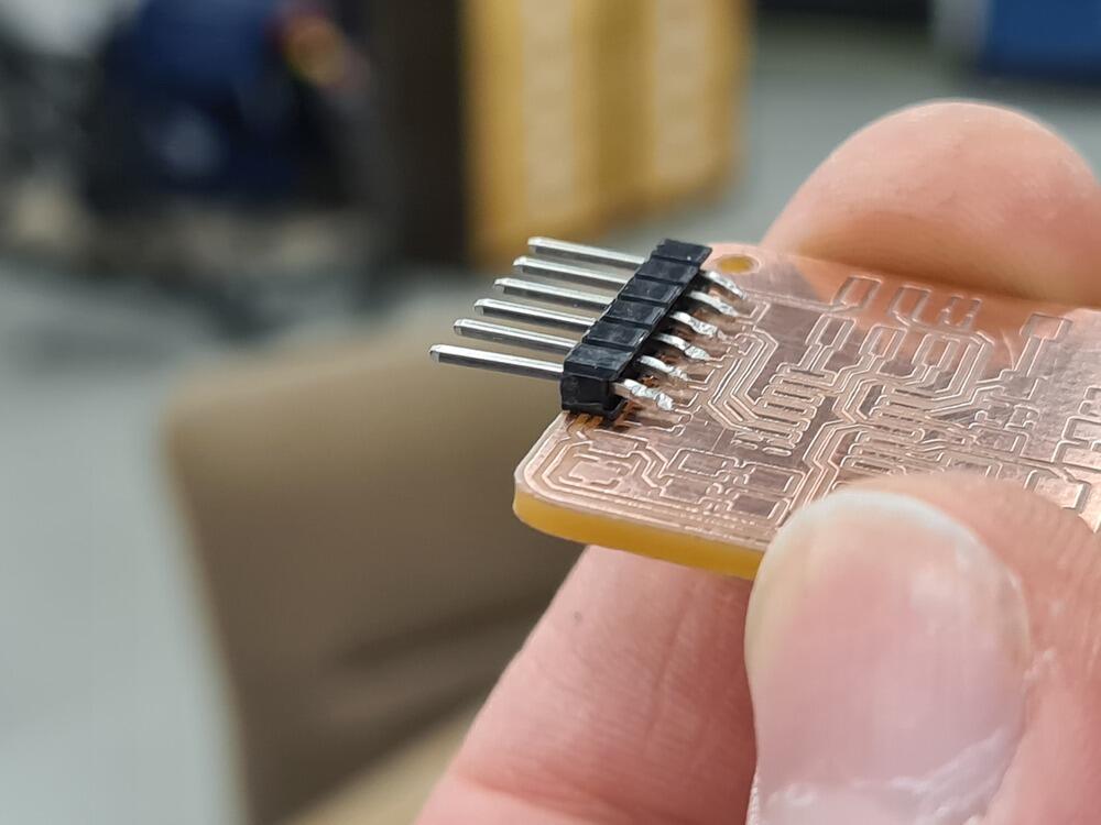
Since we didn’t have the necessary SMD headers around, I decided to wing it. Here you can see standard headers laying flat, sideways, on the PCB. Notice there is a trace running underneath the black plastic of the header:

To allow for soldering the header to the surface mount pads, i gave them a good bend by clamping them in a vice and bending the header pins over using a female header strip as counterpart…
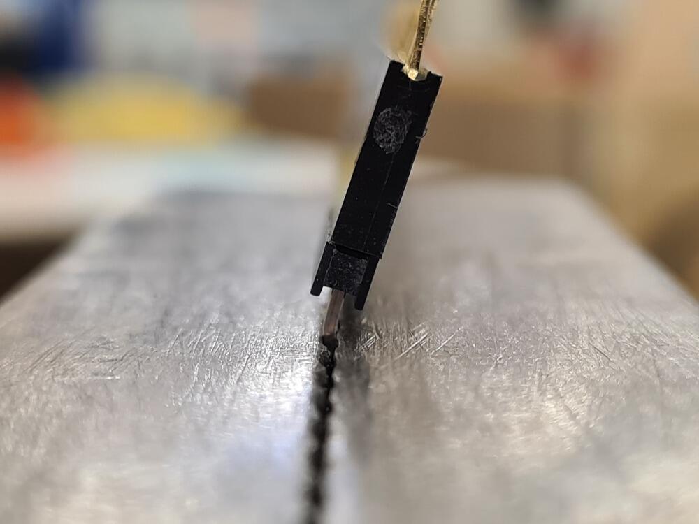
…yielding a slight bend to the end of the pins…
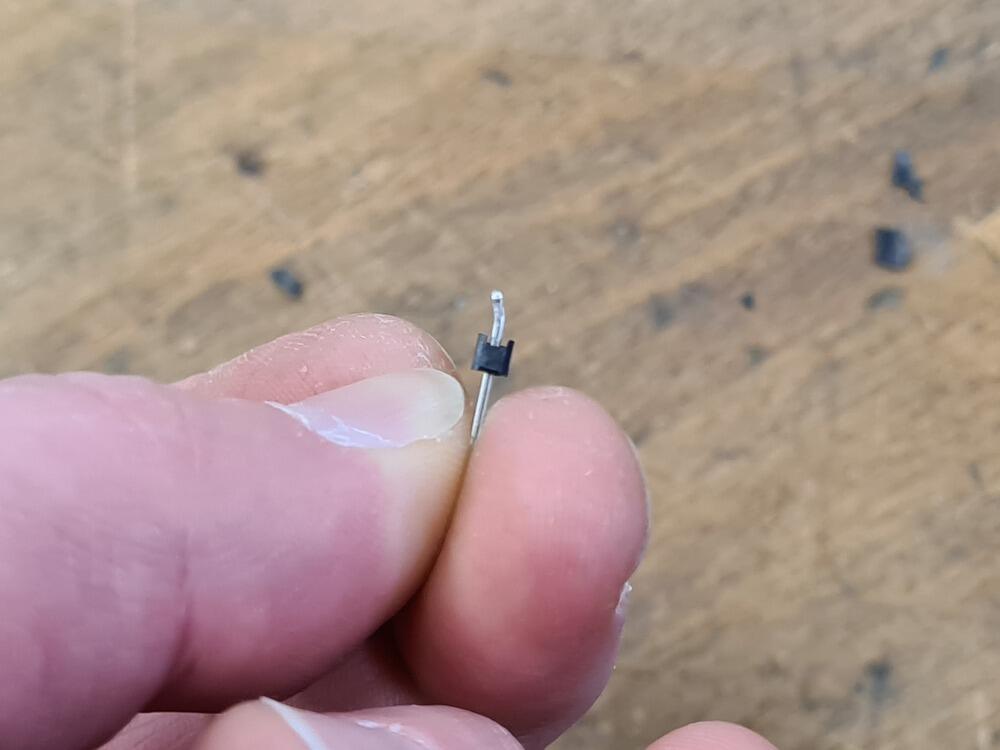
…just enough to make them nearly touch the soldering pads:
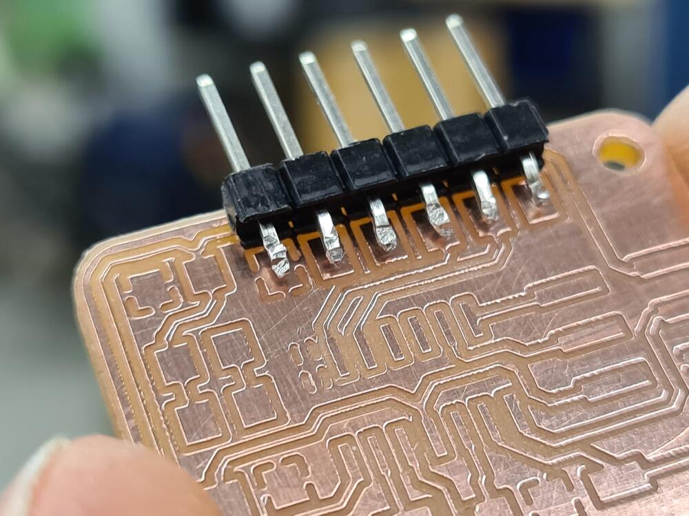
Using another piece of PCB stock to just hold the header up…
…I first glued the black plastic of the header down to the PCB using two-component, five minute epoxy glue:
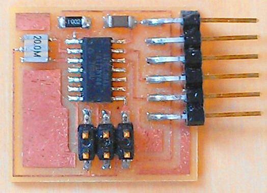
With this out of the way, I stuffed and soldered the rest of the board (and the headers, as well). After checking for shorts between 5V and GND, I applied power using an FTDI cable on the FTDI header. Here it is during power test, with the power LED lighting up as expected:
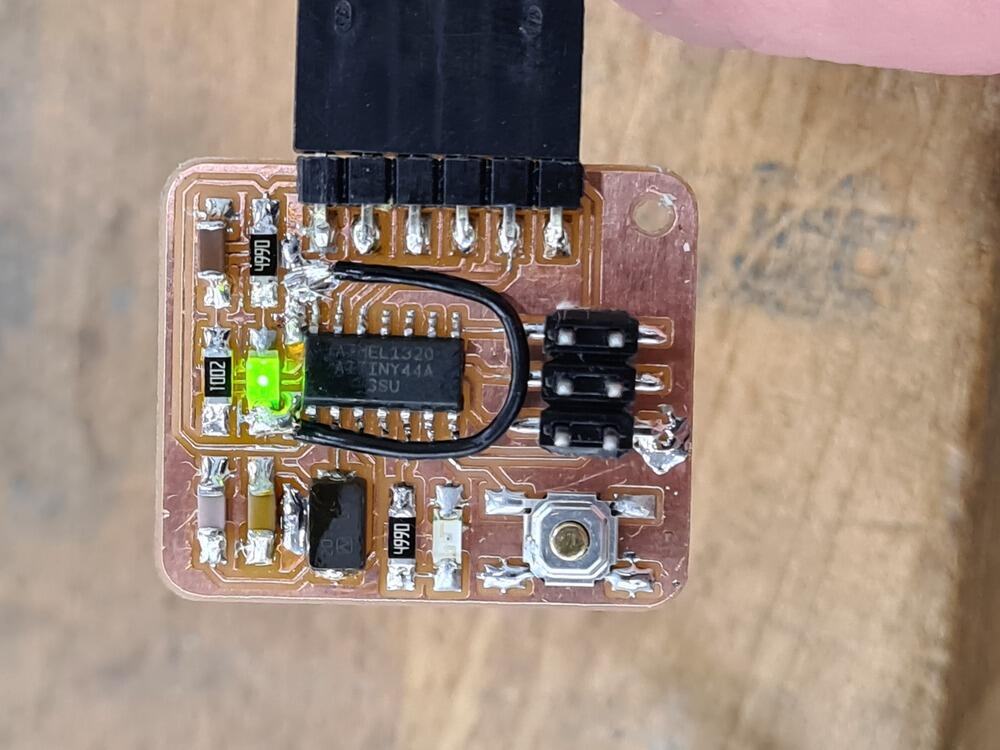
Here another perspective showing how the headers turned out. Not too shabby, I must say. There shouldn’t be any strain on the copper pads, as the epoxy glue secures the header well in place:
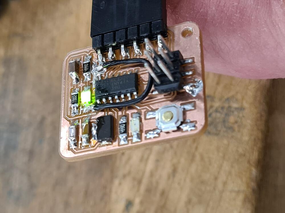
I then washed the whole PCB in some 99% Isopropanol by just swirling it, to get rid of all the flux gunk from soldering:

Here, again, is also the final schematic designed for the board:
Testing the Board
Programming
To test the board, I first had to program it. Lacking a proper ISP programmer, I decided to use an Arduino as ISP programmer. In the Arduino IDE, I selected my board…
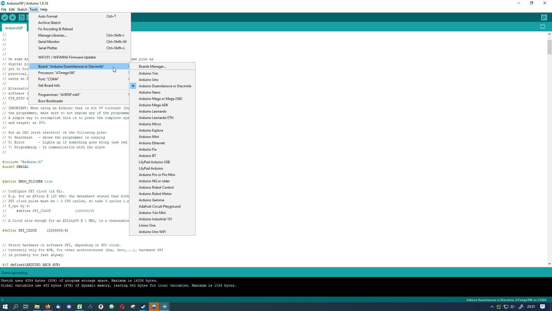
…which was an Arduino Duemilanove (yes, old!):
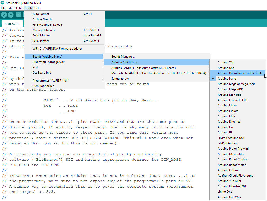
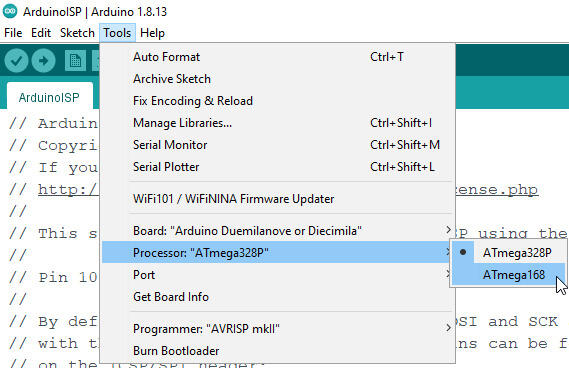
It even still uses an ATmega 168, so I selected that…
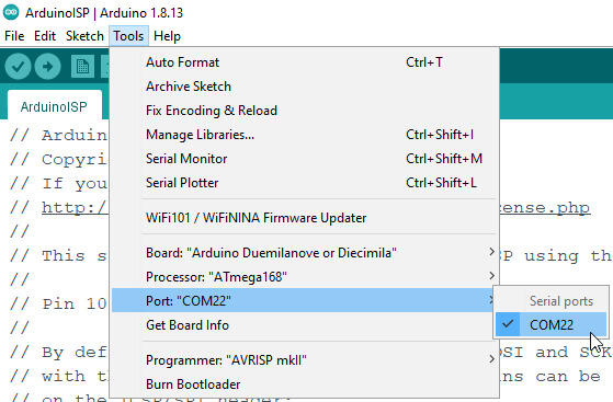
…and the right COM port where it was connected:
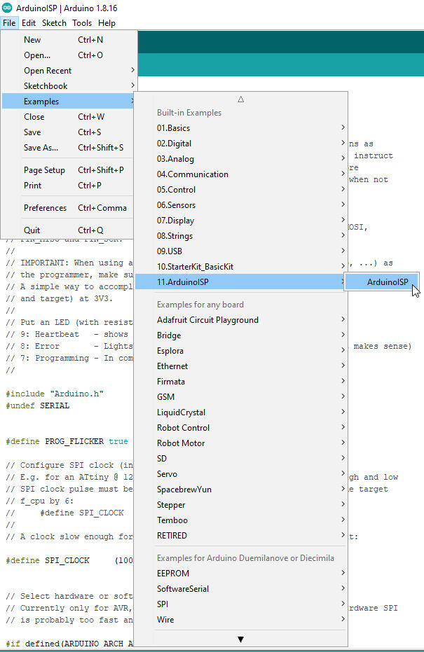
I then opened the ArduinoISP sketch provided in the Arduino Examples…
…which looked like that:
Using the button Upload, I compiled and uploaded the sketch to my Arduino Duemilanove, essentially turning it into a simple ISP Programmer:
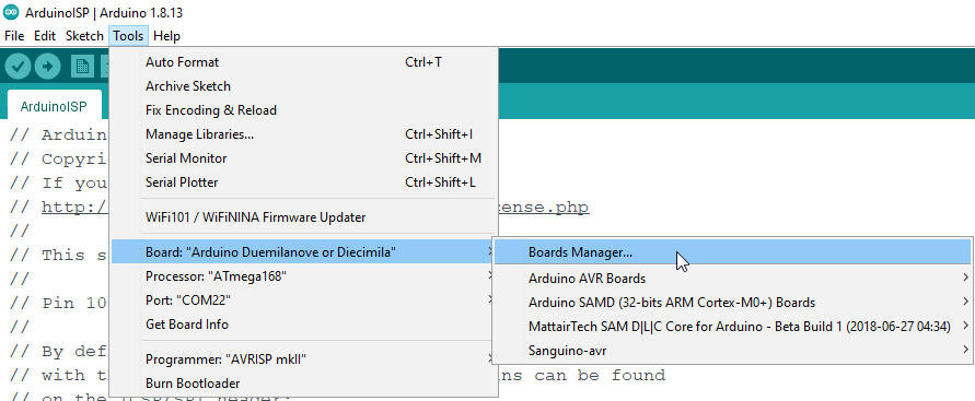
With the programmer sorted, I now had to take care of the programmee, my modified ATTiny44 Echo Board. Since ATTinys aren’t generally supported in the Arduino IDE, I installed an additional URL for the board manager (by David Mellis, on Github)…
…then opened the Boards Manager…
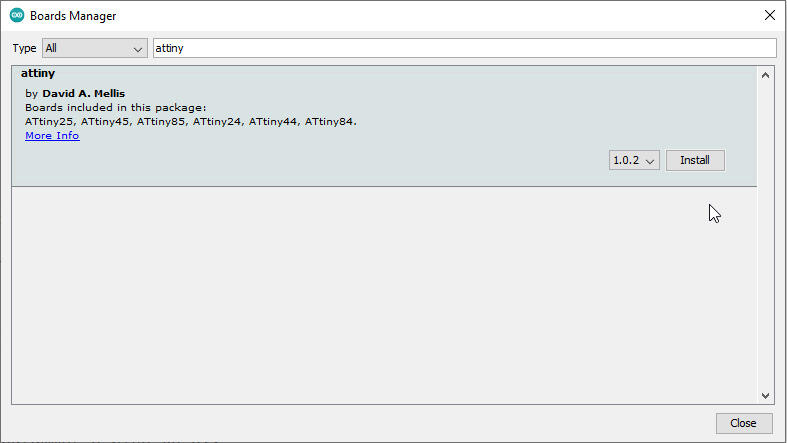
…and searched for (and then installed) the attiny package for adding support for ATTiny boards:
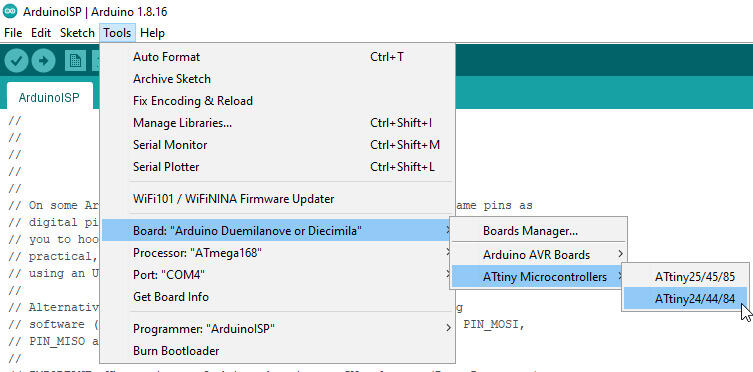
Afterwards, the ATTiny44 could be selected as a board from the board selection menu:
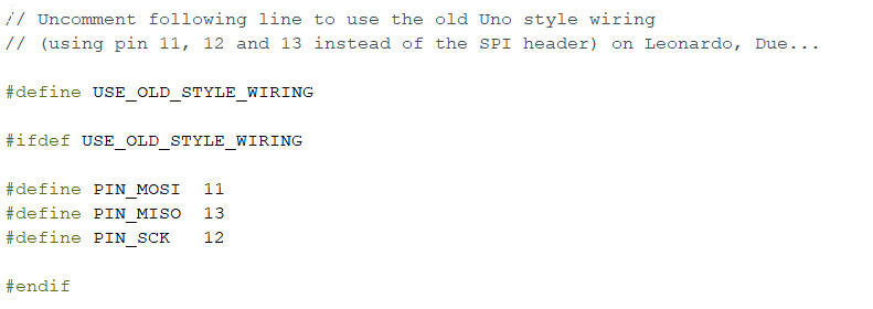
In the ArduinoISP sketch, I then also realized I needed to use the old style wiring method as described in the (commented) sketch itself, so I uncommented the #define USE_OLD_STYLE_WIRING. For some reason, in the cable I had available for making the ISP connection, there was a twist, too, so I had to swap the MISO and MOSI pins in code (I then reuploaded to the Arduino Duemilanove):
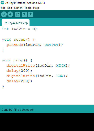
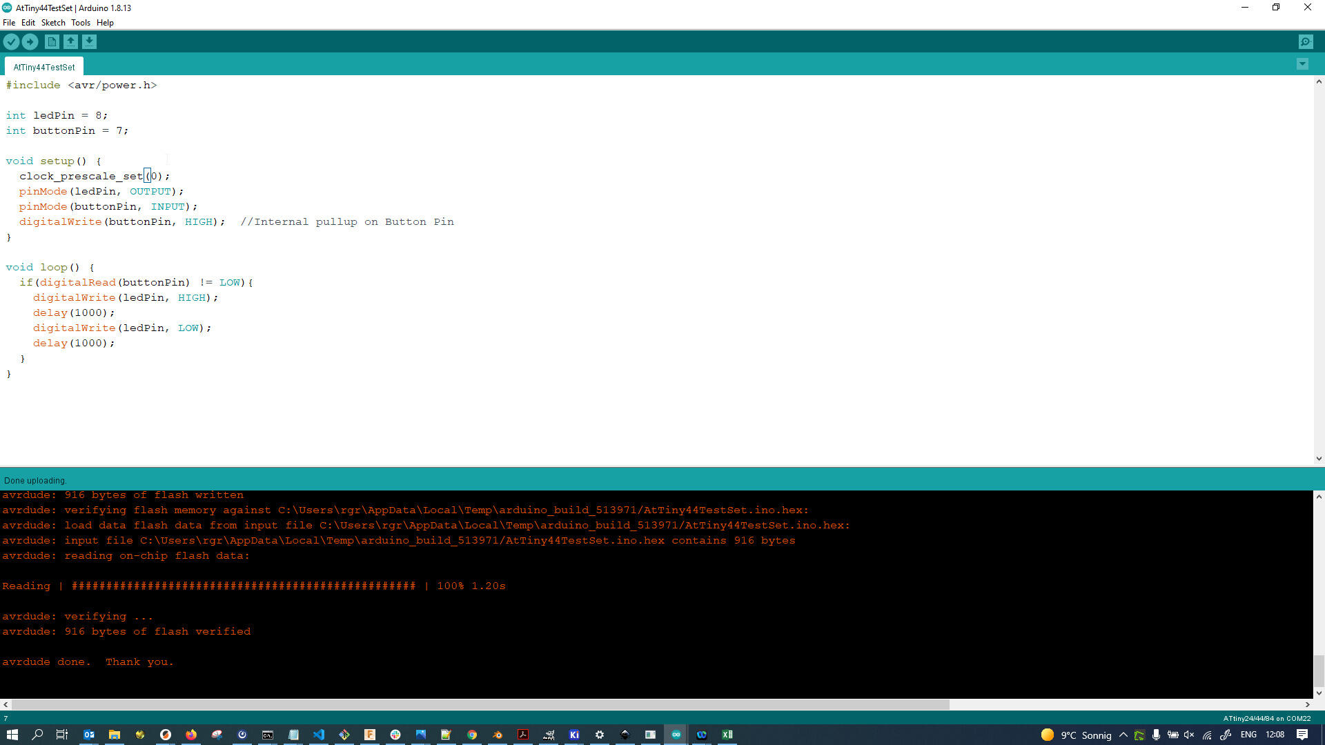
I whipped up some tiny piece of code for the ATTiny44 Echo Board that would just blink the LED I had added on PB2:
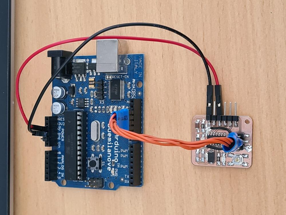
Here is the programming setup, with the blue Arduino Duemilanove acting as an ISP programmer, with its pins (as defined in the ArduinoISP sketch) connected to the respective pins on the ATTiny44 Echo Board. Power and GND were supplied using two jumper wires going into the FTDI header, as the blue heatshrink tubing on my cable prevented me from using all 6 pins on the 2x3 ISP header:
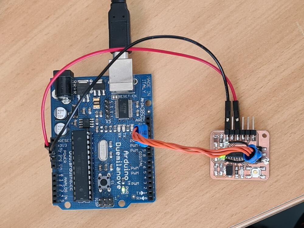
I then applied power via USB and programmed the ATTiny44 Echo Board by pressing Sketch -> Upload Using Programmer - it worked. And: no smoke… but also: no blink:
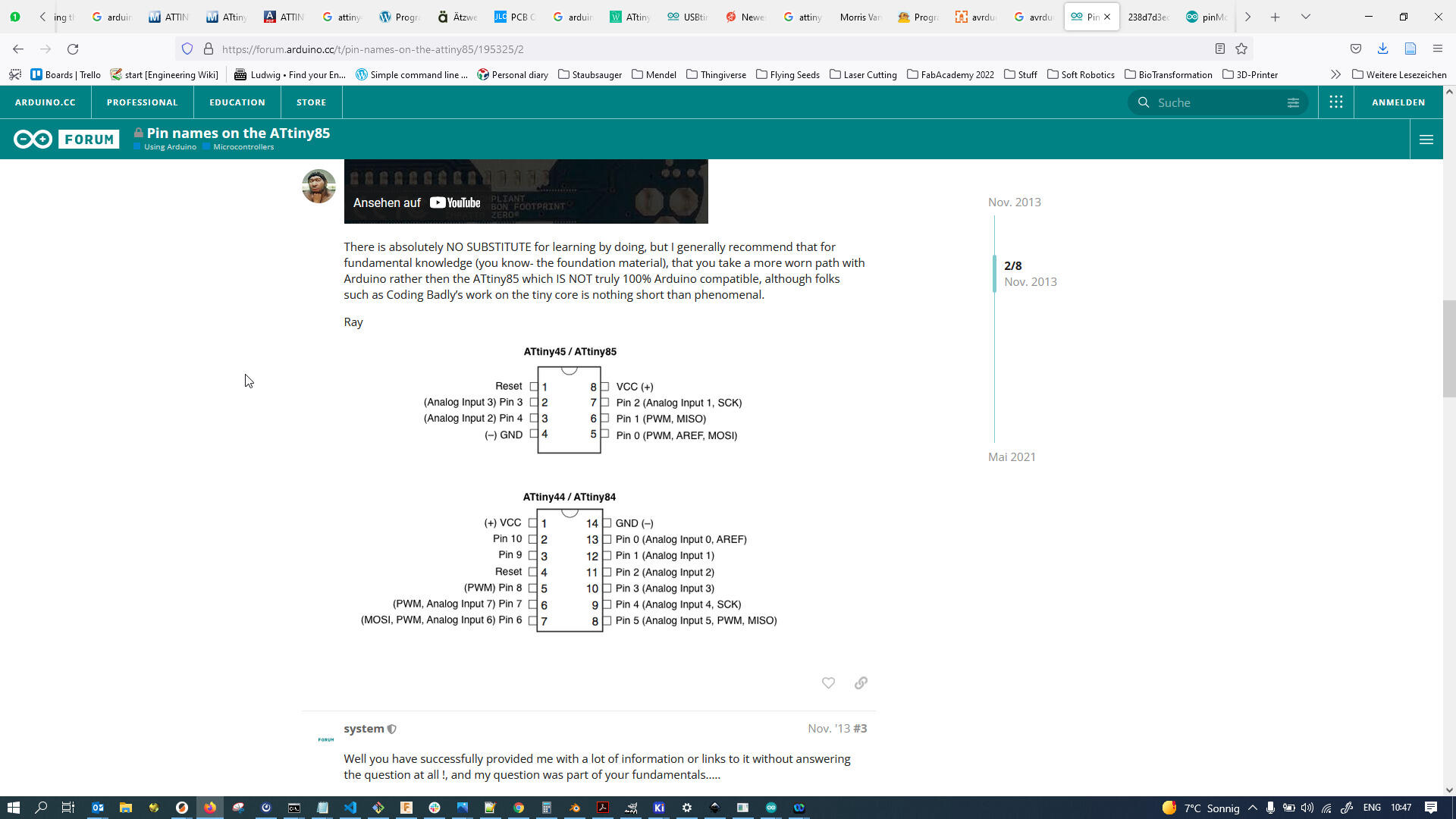
I then realized I had gone with the wrong pin number for the LED in my simple test. The ATTIny pin names are not the same as the Arduino pin names. Following table shows that PB2 on the ATTiny is actually called 8 in Arduino Terms:
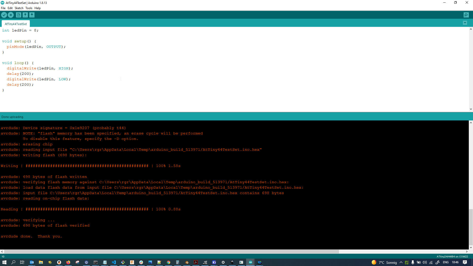
After changing the pin number to 8 and reuploading (notice the successful programming console output, too)…
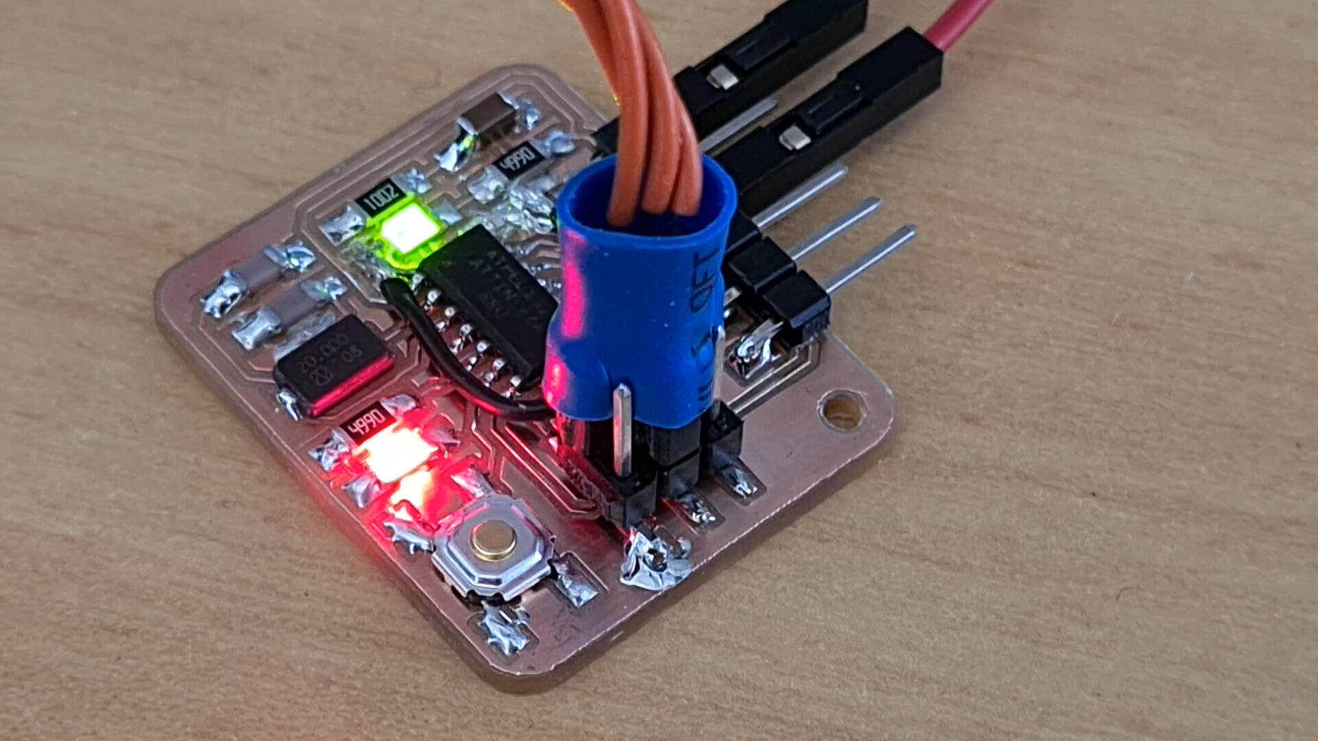
…the board immediately started blinking after flashing the program:
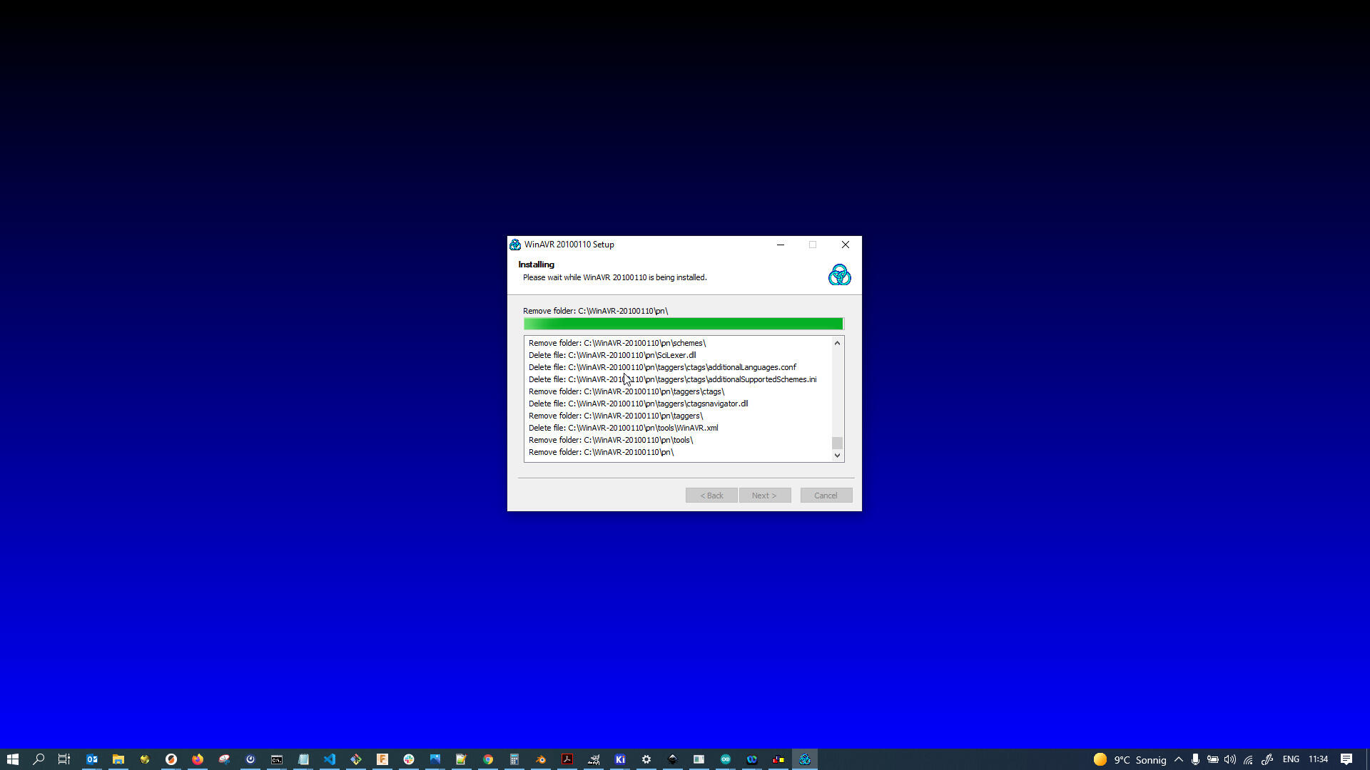
The board flashed at a wrong pace though, so I downloaded the WinAVR suite…
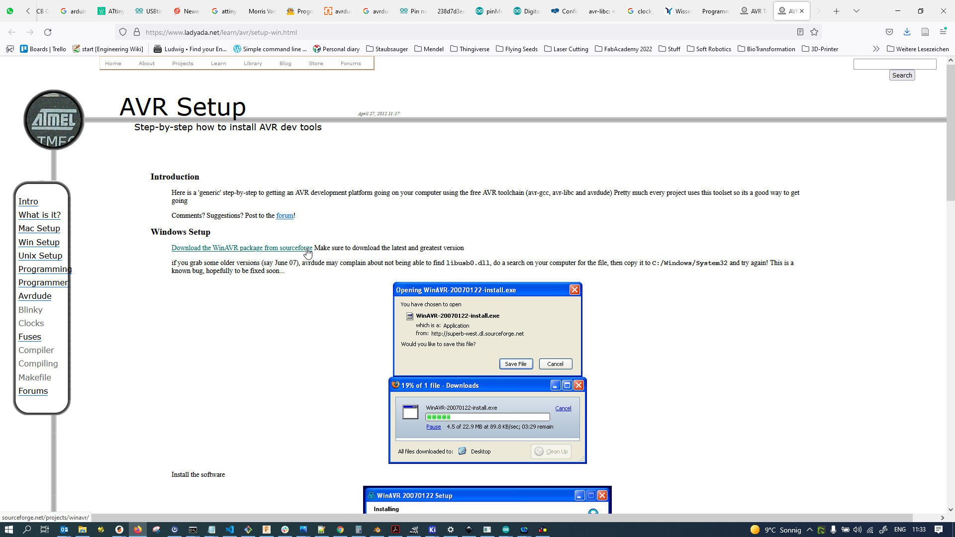
…version 20100110…
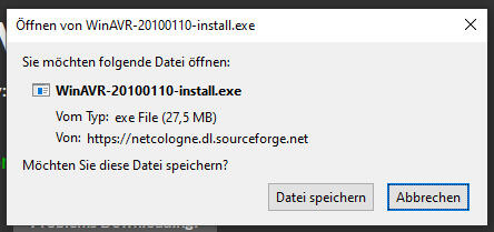
…and installed it:
Adding the function call clock_prescale_set(0) into my setup function fixed the problem for me and the board was blinking at the proper pace now:
Testing
I then went ahead and opened up Neil’s HelloFTDI44Echo code onto the device. Flashing the firmware went perfectly fine:
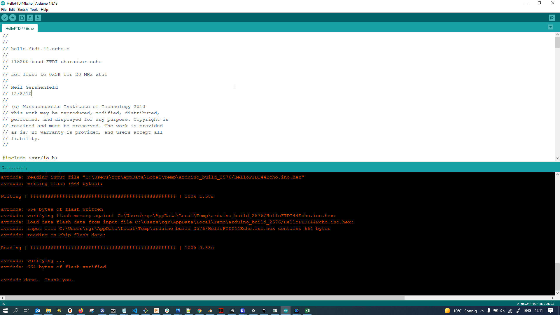
I then connected the ATTiny44 Echo board on its own to my computer using an FTDI cable (USB-Serial converter):
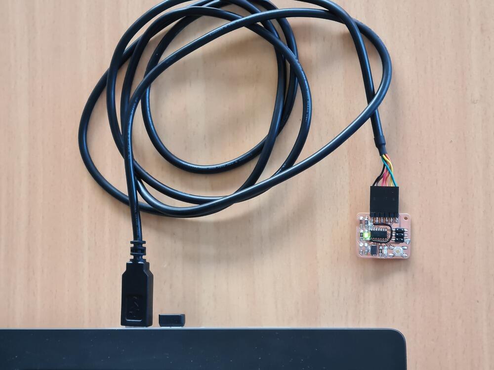
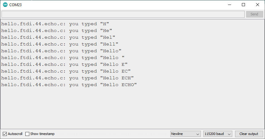
Upon typing on the Serial Port, the ATTiny44 Echo board sent back the characters on the Serial Console, as was expected. Everything worked:
Design Files
-
Neil Gershenfeld’s HelloFTDI44Echo Code in Arduino IDE (INO, Arduino IDE)
-
Redrawn and modified ATTiny44 Echo board (KICAD_PRO/KICAD_SCH/KICAD_PCB, KiCad 6.0)