5. Electronics production
Background - Electronics production
- Years back: Using toner transfer method to make boards in the basement
- Etching with Iron(III) chloride
- Drilling holes with a handheld Dremel tool (with flexible shaft - much better!)
Group Work
This is a quick series of events that happened in our first days of working with the machine(s). A more detailed (probably) account can be found on the group assignment webpage.
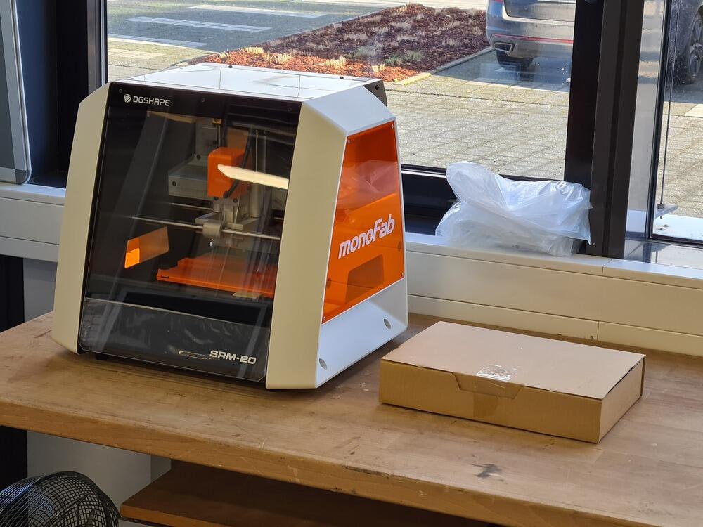
Day 1: The SRM20 Debacle
- We unpacked and setup the machine
- Then, a realization: there was only a 6mm collet!, but: most tools we have around are 1/8”…
- Another realization: These collets are expensive! Going by our orders, we should have a 1/8” collet around, but that might have gone to Ghana…
- An evening internet search yielded: There’s a multitude of different collets for the SRM20 (all of them ~$70), there are also 6 mm to 1/8” adapters and Roland itself offers an official Engraving Kit for the SRM20, that besides the collet also has standoffs for the bed, so shorter engraving tools can reach the material on the bed.
The Roland SRM20, fresh out of its box.
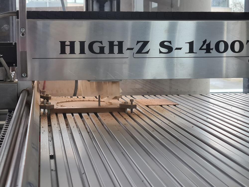
Day 2: The Big Guns
- With the SRM20 unusable for us in its current state, we made our big CNC mill accessible, clean and ready to cut
- This one, even though overkill space wise, has in the past produced very nice, tiny boards. It is a very weird feeling to produce a 50 x 50 mm PCB on a machine of that size :)
- We added an underlay to the work stage and milled it flat using a 6 mm mill bit and some code quickly whipped up in Fusion 360. We assigned coordinate system G59 to our little corner of the CNC that we planned to use for PCBs from now on (there is a little notch for registration with [0,0] in the underlay).
The CNC-Step High-Z S-1400T leveling an underlay for PCB manufacturing.
Day 2: The Chinese Needle
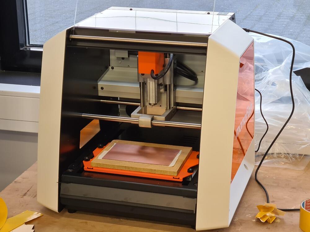
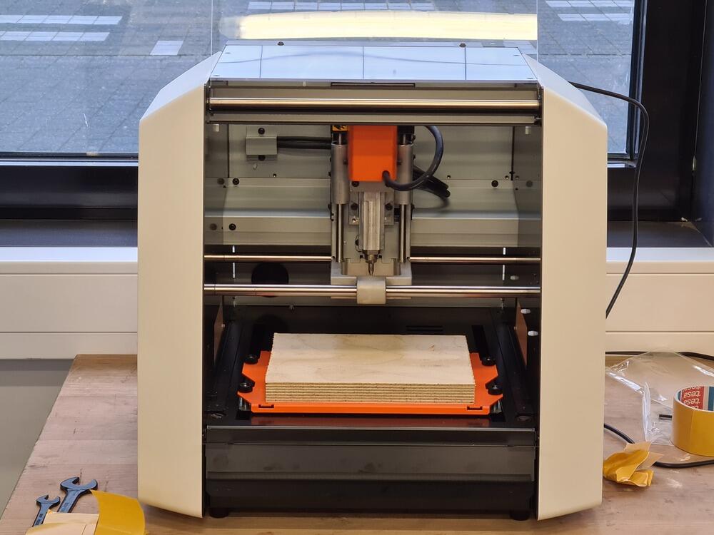
- In parallel, we also revived a Genmitsu CNC 3018 that was gathering dust sitting unused in the workshop for a while
- First, we had to figure out the toolchain, which ended up being Mods for creating the (standard) Gcode and Candle for streaming the Gcode to the machine
- After working out the toolchain: Turns out to be a reliable little mill, even though the USB connection board-wise is super flaky, so no cables should be touched while running a job…
- Over the day, this little mill actually churned out 3 programmer boards!
Day 2: Big in Japan?
- While Setting up the big CNC mill, Aaron Hinkle turned a 6 mm to 1/8” adapter on the lathe (from an M10 screw, turning down for an exact fit, then adding the 1/8” center bore and adding a radial hole for passing through a set screw from the outside (through the 6 mm collet). The set screw hole was drilled on our big, manual mill.
- The original set screw was too short, so an M4 bolt was cut down and given a slot for a flathead screwdriver using the bandsaw
- The adapter could now be inserted into the collet and the set screw holes aligned. The tool could then be inserted into the adapter an set in place with the longer set screw
- After that, the Roland SRM20 was also ready to use with our 1/8” bits!
Aaron Hinkle‘s phenomenal 6 mm to 1/8” collet adapter, with M4 bolt for a set screw…
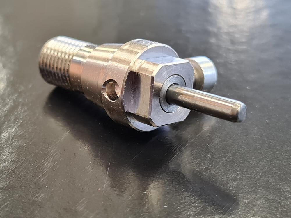
…which did strike us as too janky to actually put on the machine in the end - it was replaced by an M4 set screw fabricated from an M4 bolt by cutting it down and cutting a slot using the bandsaw (shown with a broken tool as a proxy):
Day 2: A Recap
After spending the whole day in the lab, we were happy to see that we now had 3 mills in immediate working order to mill PCBs with. In the end, we didn’t use the big CNC, since we wanted to figure out the small scale mills’ toolchains first, but it is good to know that the big one is prepared for big scale milling week, too. And it could still be used for making PCBs if needed. Big ones :)
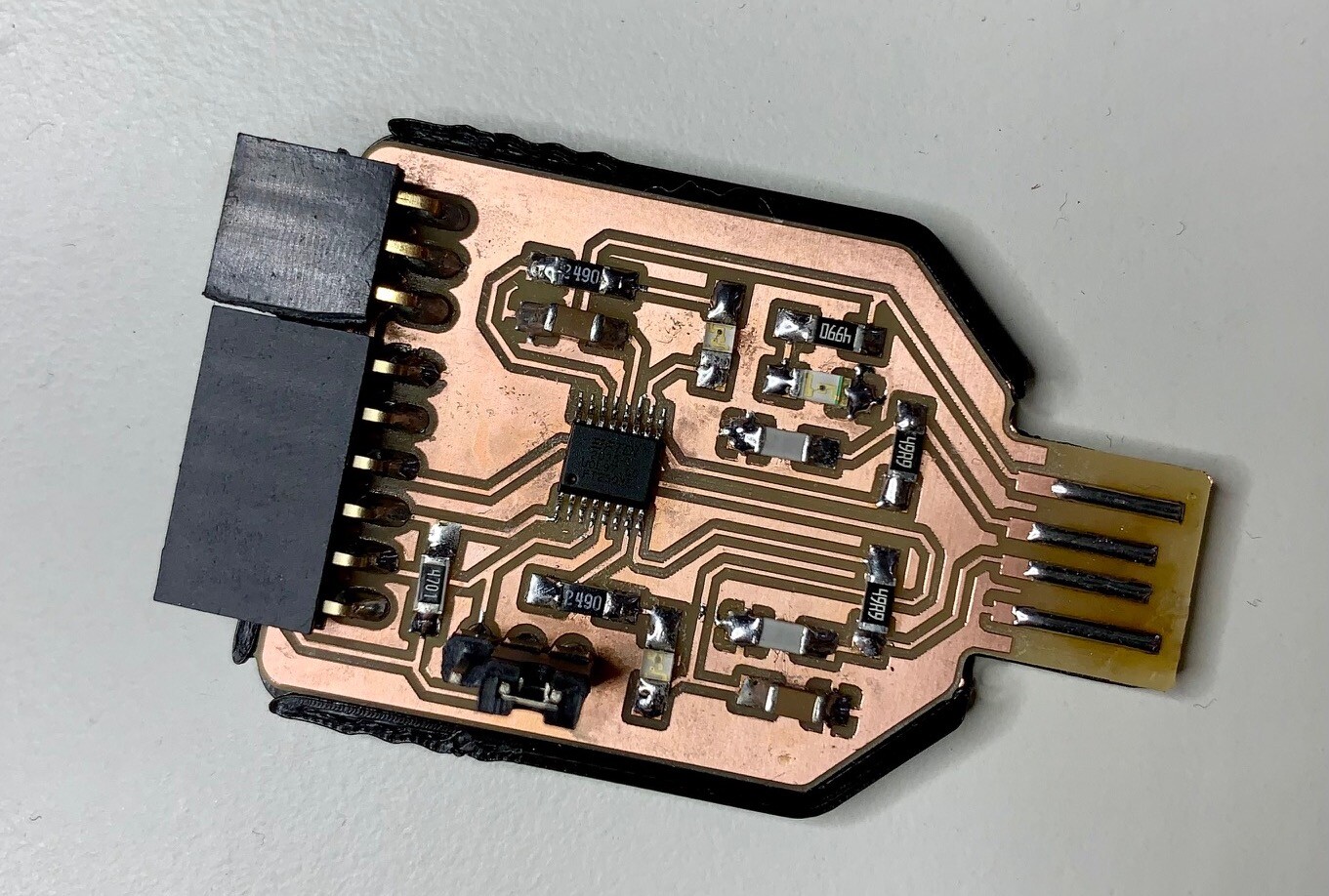
Day 3: Making a Programmer Boards
For my very own programmer board, I decided on making the FT230x-UPDI designed by Ahmed Abdellatif from FabLab Kamp-Lintfort, Germany. I figured that even in the worst case scenario - me picking a processor for the final project that didn’t talk the UPDI programming protocol - I’d still have an FTDI USB-Serial converter to work with - those come in handy all the time.
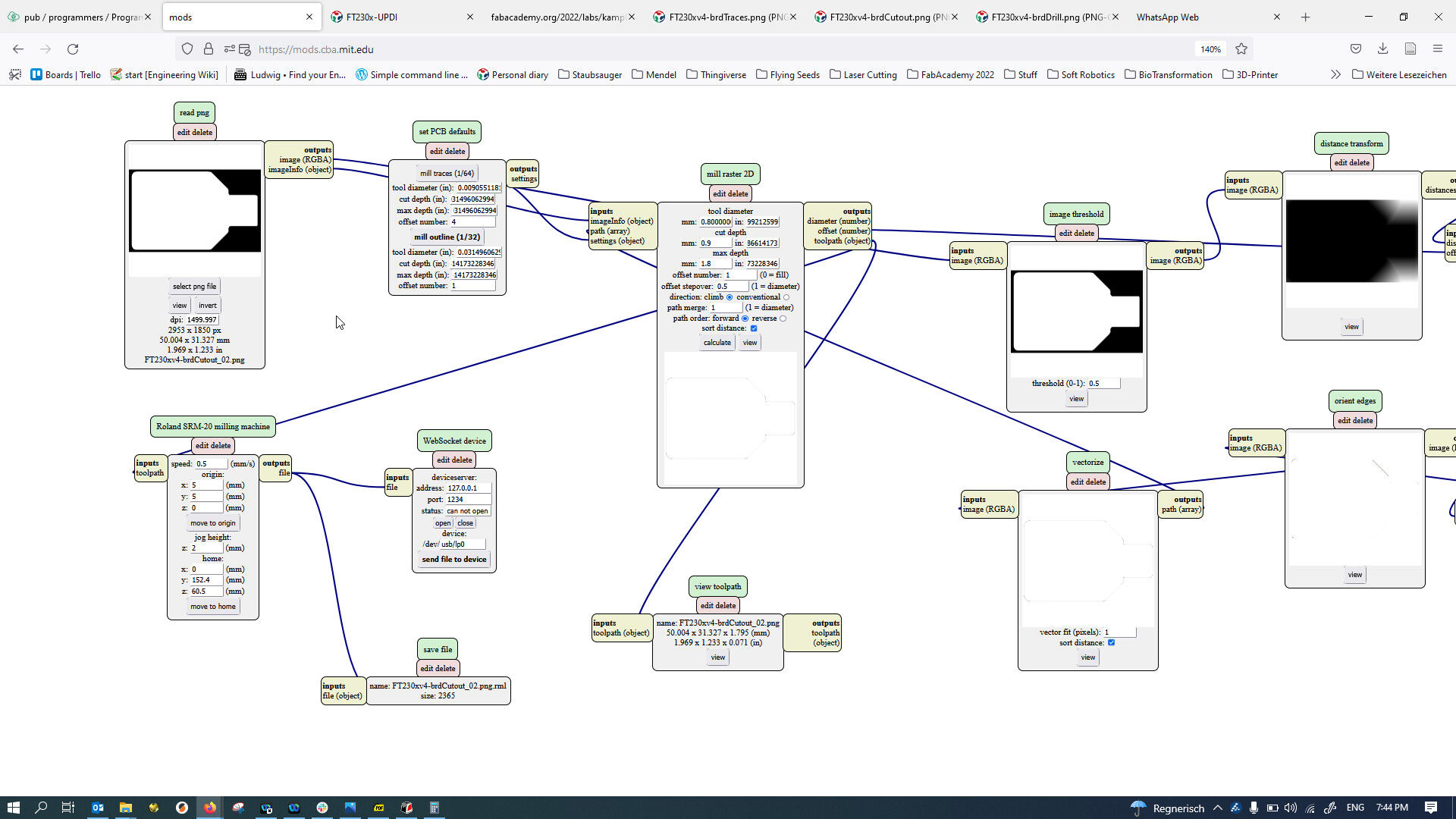
To begin with, I downloaded the necessary PNG files for the board traces and outline from the board project’s website. I then opened Mods and loaded up the node workflow for generating machine code for the Roland SRM20 by clicking RMB -> programs -> open server program -> machines -> Roland -> mill -> SRM20 -> PCB png.
![]()
Mods provides many different workflows by graphically connecting the outputs of program nodes to the input of other nodes to perform multiple, sequential operations on e.g. an input image. For the PCB png workflow, the user loads a PNG image which then gets vectorized. The vectors representing the board traces are then offset for a specific tool size so that the cut paths actually leave behind the desired copper traces. The cut paths can then be exported in various formats, like Gcode or Roland’s RML format.
Subsequently, I loaded the PNG for the traces and the PNG for the cutout into Mods and prepared milling paths using following setup values:
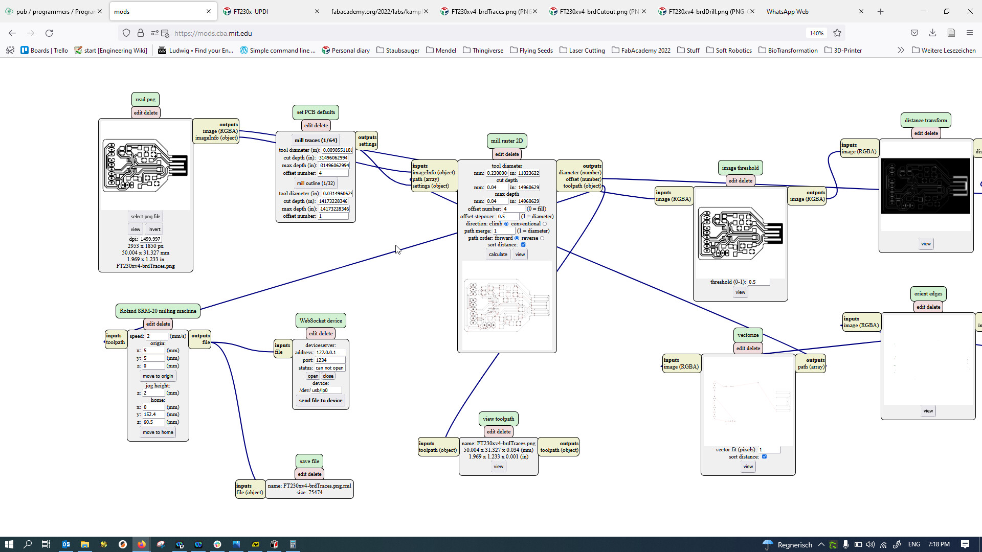
| Parameter | Traces | Outline |
|---|---|---|
| Tool Diameter | 0.23 mm | 0.8 mm |
| Cut Depth (mm) | 0.04 mm | 0.6 mm |
| Max Depth (mm) | 0.04 mm | 1.8 mm |
| Offset Number | 4 | 1 |
| Offset Stepover | 0.5 | 0.5 |
| Direction | climb | climb |
| Path merge | 1 | 1 |
| Path order | forward | forward |
| Sort Distance | true | true |
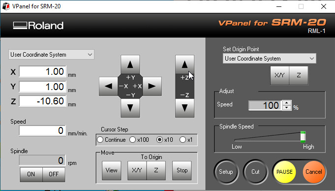
The Mods program output RML files, which can be opened in VPanel for SRM20, the control program for the SRM20 mill and streamed to the machine from there. Alternatively, it seems like Mods could also control the machine directly, but I did not investigate this route yet.
I used TESA brand double stick tape to fix a sacrificial underlay of XYZ mm thick MDF to the Y-stage of the SRM20, only to then realize that a PCB mill bit inserted in the spindle would not be able to actually even reach that far down on the platform. A quick internet search showed that this is not uncommon, as PCB mill bits and/or engraving tools often have much shorter shafts than proper mill bits, meaning that in combination with a thin underlay, the tool tip might not be able to reach the workpiece surface before reaching maximum Z-travel of the spindle. In fact, Roland offers an engraving kit for the SRM20 that not only contains the proper sized 1/8” inch collet for most engraving tools’ shaft size, it also contains standoffs to prop up the Y-stage to compensate for the shorter reach of the tools.
In our case, since we had the 6 mm to 1/8” adapter for the collet now installed, we simply installed a thicker Multiplex underlay to allow the tool tip to reach the PCB to be milled.
After sticking down the Multiplex underlay using TESA brand double stick tape, I used the 3 mm (6 mm shaft) mill bit supplied with the SRM20 to level the top surface of the underlay. I first tried to generate a tool path using Mods, too, but that was unsuccessful. Mods refused to load the PNG image I prepared in Inkscape for leveling off the large area to begin with. I then found out that loading the image did work using Chrome instead of Firefox, though the paths would still not generate. Doing a little bit of research, I found out that the Roland SRM20 software suite also included a handy little tool called ClickMill that allows for running simple operations, like drilling holes, making cutouts and also leveling in a very simple and direct way, without preparing cut files beforehand. There is a graphical wizard for generating the leveling cut, which worked fine for the setup. There was a very weird behaviour though: Even though ClickMill was instructed to perform a 1 mm deep leveling cut and Z0, the zero coordinate of the mill, was set to the top of the workpiece, when starting the leveling cut, the mill would not actually plunge into the material at all. It would just perform the leveling cut path at height 0, essentially not cutting anything at all. Since the whole leveling cut was going to take quite some time, the cut was aborted and the mill’s Z0 was manually set to 1 mm into the material (off the edge of the material to allow the bit to plunge lower that the top surface). When restarting the same leveling cut that showed the odd behaviour, it still did run a full pass at height Z0, which, now being 1 mm below the top surface, did remove the top first mm of the board. When the whole top layer had been cleared, the mill did actually try to plunge down 1 mm for another pass, but the cut was aborted at that point, since the leveling had already taken place. Given how long clearing out a big area like that takes, it is a very weird design decision of Roland’s software engineers to first make a full level cut at a height where nothing would be cut, only to plunge down afterwards for the actual cut - unless I messed up the parameters good (which seems unlikely given how the GUI presents things) and totally got it all wrong.
After leveling the underlay, I placed a one-sided PCB blank (FR1 or FR2) onto the underlay, registering it with the corner that had been cut into the underlay while leveling. The PCB was fixed to the underlay by - again - using strips of TESA brand double stick tape, trying to minimize bubbles in the tape as much as possible and cleaning both underlay and PCB well beforehand to avoid debris getting caught under the tape.
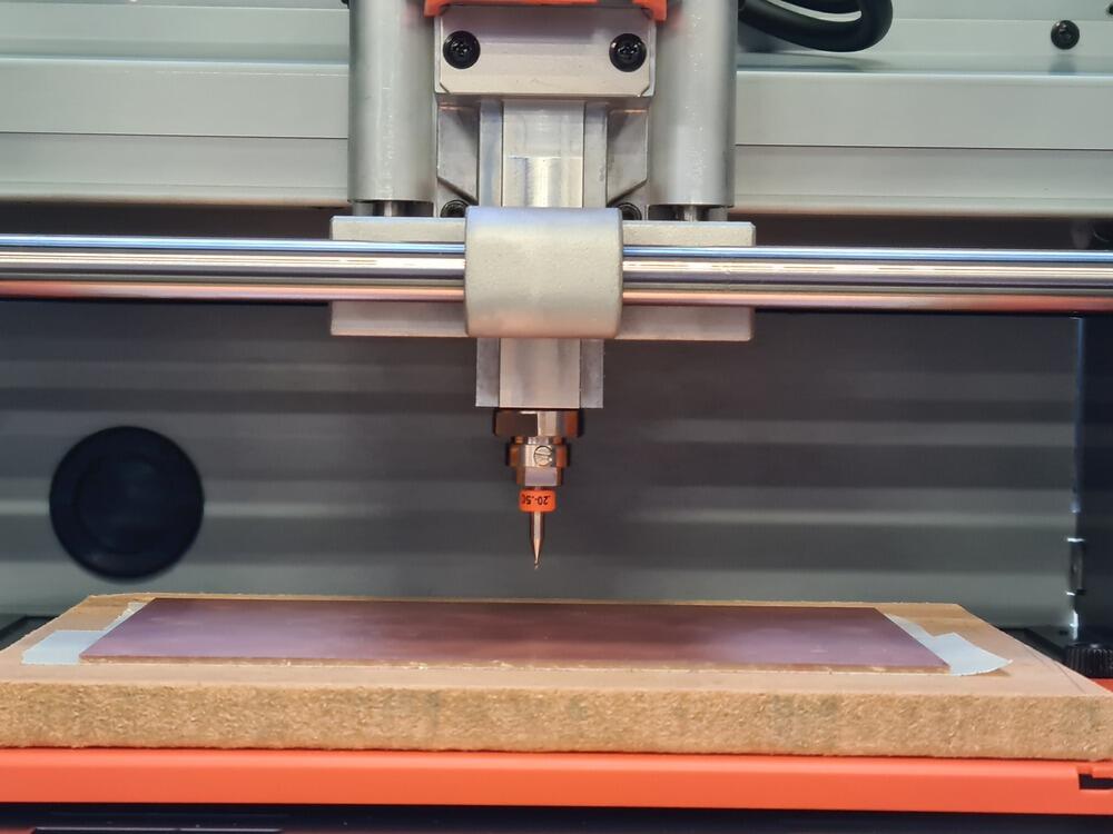
After attaching the PCB blank, I inserted a 0.20 - 0.50 mm PCB mill into the collet with the adapter. With the spindle turned on and running at 100% speed, I slowly lowered the mill bit down towards the PCB surface, first going in steps of 1 mm, then 0.1 mm and ultimately 0.001 mm. As soon as I started hearing the mill bit cutting and seeing the first signs of debris coming off the tip of the mill bit, I set this height to be Z0 - essentially this would not exactly be the top of the PCB, but slightly underneath it. For testing, I used XY-coordinate [1 mm, 1 mm]. Whenever setting up Z0 later, I would use XY-coordinate [1 mm, 1 + x * 2 mm], meaning that the second and third Z0 probings would be made at [1 mm, 3 mm] and [1 mm, 5 mm], respectively. My Gcode in Mods was all created using an XY-position of [5 mm, 5 mm] for the lower left starting point, meaning that I had plenty space between the blank PCB edge and the board to be cut edge to play with.

I then ran the Gcode for milling out my board’s traces. While milling, I had the suspicion that the copper hadn’t been milled fully through in some spaces, but this was mostly due to a very disappointing fact: the Roland SRM20 does not contain any internal milling chamber illumination - an interesting design decision for a multi-thousand dollar mill for sure! WHen the traces where finished cutting, upon closer inspection, the traces were actually cut through, though there are a few tiny spots where not all copper had been removed. With the multiple offsets used for the isolation routing though, this was still isolated an no problem.

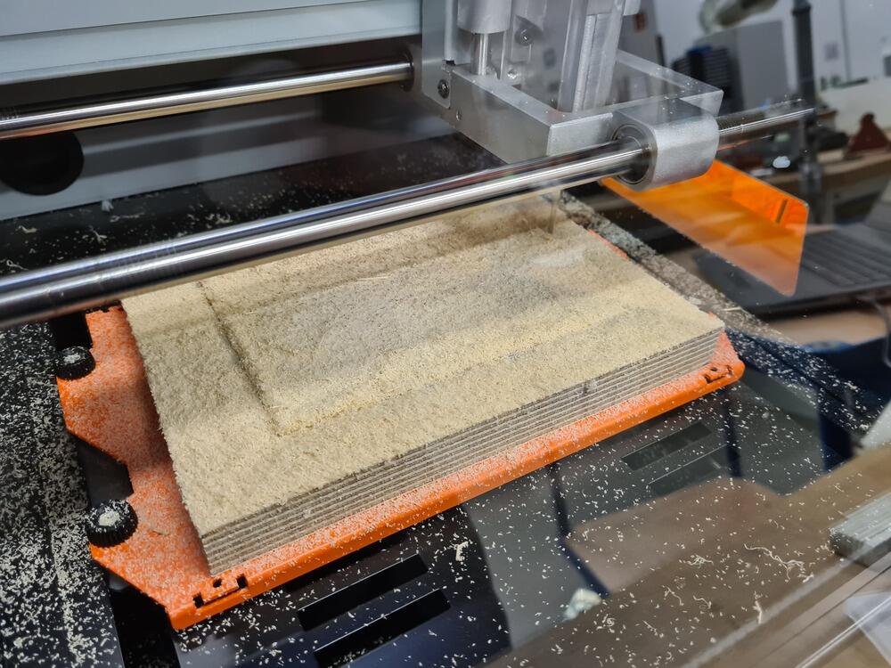
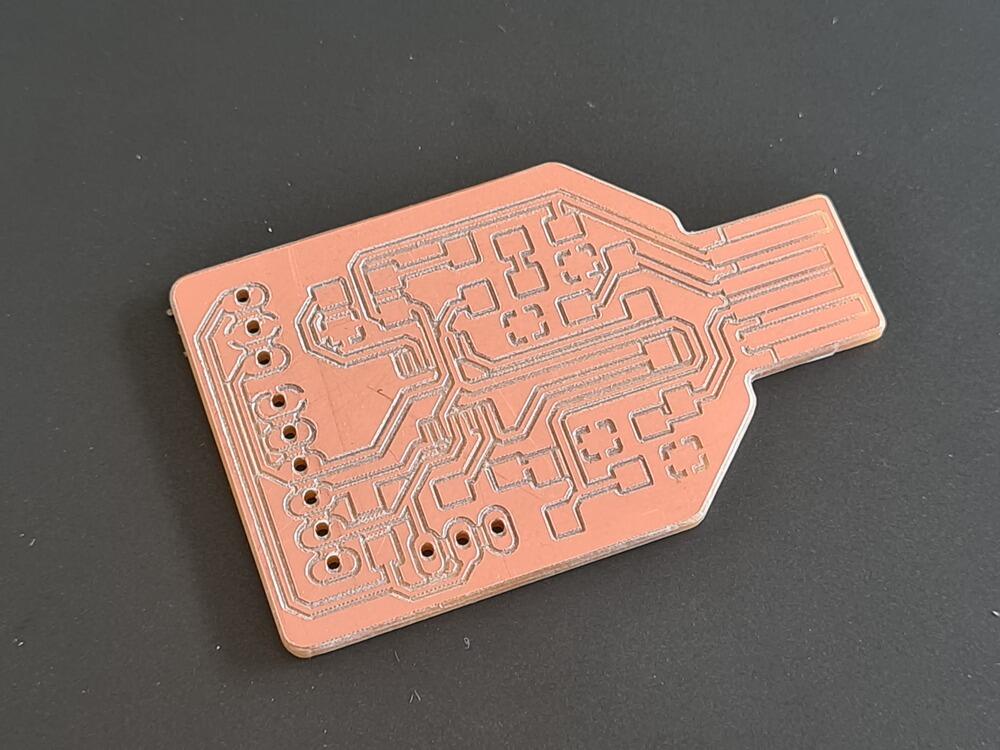
After cutting the traces, I swapped out the PCB bit for a 0.8 mm straight flute bit. After setting Z0 again, I loaded up the board outline Gcode and cut it, cutting through the whole PCB thickness in 2 cuts of 0.9 mm depth each. THe machine did pull through okay, but the table was vibrating slightly and I got the feeling that next time I’d rather try three passes at 0.6 mm depth each to lower the stress on the cutter a bit. The outline did cut fine, though the cutter did produce some curly swarf on the outside of the cut (towards the PCB blank) and the edge of the PCB backing was also slightly frizzy - this was quickly remedied by scraping the edge of a box cutter along the edge though. In the end I was left with a very satisfyingly looking edge.

Here’s a closeup of the board’s traces, not perfect yet, so the cutting values suggested to us by the local instructors might still need some fudging. In hindsight, this was rectified later by empirically determining better parameters for our mill-tool combo:

This concluded the milling of the board. For electronics, while we have most of the things (resistors, capacitors, LEDs) in our own little FabLab, we had to wait for a few days for supplies (FTDI chips, angled pin headers) to arrive from our hosting sister lab in Kamp-Lintfort. In the end, transferring the supplies was too rushed, so we had to shift our actual stuffing and soldering for the next week, when we will go to the KaLi FabLab for 3D-scanning, anyways. Therefore, there are no pictures of finished boards to be seen here!
Day 6: Addendum: Another Programmer Board
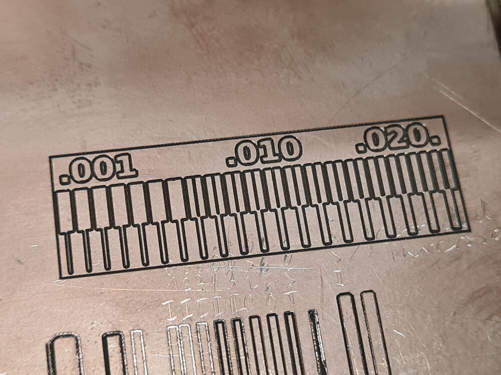
Since I wasn’t entirely happy with the cutting quality at that point, I decided to start from scratch and more methodically went through finding proper parameters for our very combination of mill and “0.20-0.50” (whatever that might mean) PCB mill bits. The detailed chronology of tests can be found in the group assignment page and yielded, after many test cuts, following beautiful line test:
After going back and more methodically figuring out hte perfect cut settings on the SRM20 with our PCB mill bits, I actually went back and cut another board to test these parameters with - they had worked very well on the line test, but would they hold up for a proper board? I used Mods again to create the RML file for cutting on the Roland SRM20 using following parameters:
| Parameter | Traces | Drill | Outline |
|---|---|---|---|
| Tool Diameter | 0.20 mm | 0.8 mm | 0.8 mm |
| Cut Depth (mm) | 0.05 mm | 0.6 mm | 0.6 mm |
| Max Depth (mm) | 0.05 mm | 1.8 mm | 1.8 mm |
| Offset Number | 1 (2) | 1 | 1 |
| Offset Stepover | 0.5 | 0.5 | 0.5 |
| Direction | climb | climb | climb |
| Path merge | 1 | 1 | 1 |
| Path order | forward | forward | forward |
| Sort Distance | true | true | true |
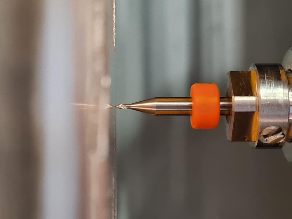
The mill bit used for cutting the board was the same as for the line test before:

Here’s a shot of the mill bit zeroed in on the board surface:
The number of offsets for the traces started out as 1, but as I saw not all copper had been cut after running the board code once, I reran the whole board with an offset of 2 (all other parameters the same) in the same place, again. This cleared out the remaining copper - which I find highly fascinating given that it doesn’t go deeper that before, just wider, but it is what it is. ¯\(ツ)/¯
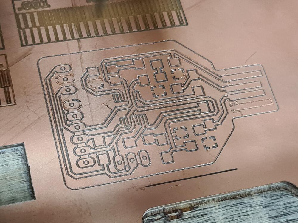
Here’s the traces after the first run - notice not all of them have cut properly:
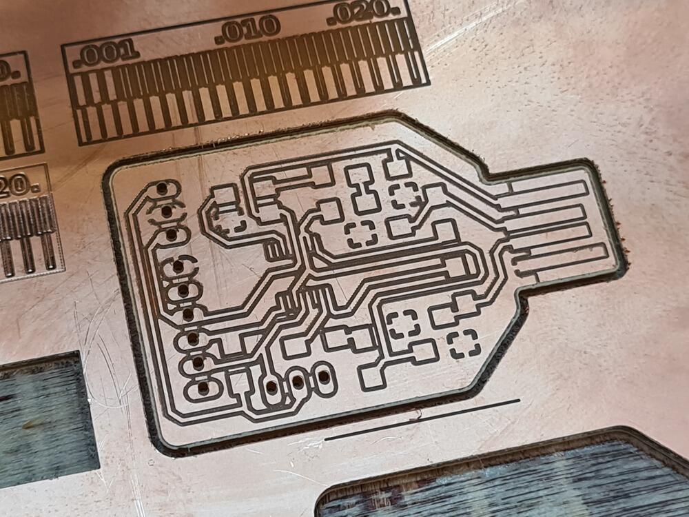
After running the traces code again in the same place using 2 offsets, alls cuts seemed to be properly made:
This time around, I also had the SRM20 drill the holes for me - with a 0.8 mm mill bit, these ~1 mm diameter holes were no problem to “milldrill” with. Unfortunately, the original design files from the KaLi project page only provided a PNG for the drill layer that was missing some of the holes to be drilled. Opening the projec tin KiCad, then exporting the layout to SVG, removing all but the holes and filling them black, then exporting just the holes at 1500 dpi for mOds to work with, worked somewhat fine. Unfortunately, I realized that I must have gotten the padding (extending the edges of the image) in Inkscape ever so slightly wrong, as the holes are aligned in X, but just slightly shifted in Y, meaning that the padding of the top/bottom edges was somewhat off.
After cutting the outline of the board, the backing material edge turned out to be a bit fuzzy from milling:
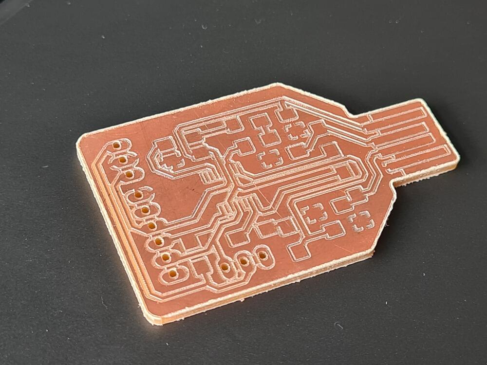
A quick scrape with the box cutter rectified that and the board had clean edges:
Lessons learnt about milling PCBs
- Shelling out $4000 for a machine that is supposed to generate very fine features and involves using tiny cutting bits does not guarantee getting light where you need it most - inside the chamber.
- Leaving even little artifacts in the input PNG files (like very slight double lines around the board edges) does produce Gcode that might have artifact, too, like little bumps on otherwise straight cut paths.
- Finding Z0 is surprisingly hard to get right. From what it feels like, going 0.035 mm (35 µm) deep from a Z-height where a cut was already made would not necessarily guarantee cutting through the whole 35 µm (as advertised…) copper, too. I felt that fudge factors where my friend here and I’d rather go 0.05 mm deep to safely isolate traces. Unfortunately, especially with the PCB mills with a V-shaped tip, this uncertainty also means that the effective tool diameter at the cut is not very determined.
Going down the Rabbit Hole - Reviving pcb2gcode
When I was first getting into milling circuit boards, I was slightly put off by the number of conversion steps - and the fact that I’d deliberately convert a vector format into a raster format to then again make vectorized cut paths out of that. Doing some research, I found the software pcb2gcode that takes gerber files and converts them into Gcode - in newer versions even using a vectorial core and thereby skipping the conversion through a raster image. Those few years back, I already found the process to be a little glitchy and IIRC, it also needed some compilation on my side, but in the end, it produced beautiful Gcode from Gerber files output by Eagle. This week, I tried to revive this old workflow of mine to generate Gcode from Gerber files generated in KiCad.
| pcb2gcodeGUI Version | pcb2gcode Version | Input | Output | Notes |
|---|---|---|---|---|
| 1.3.2-1 | 1.3.2 | KiCad 6.0 Gerber | none with Vectorial Core | precompiled binary |
| 1.3.3 | 2.2.0 | KiCad 6.0 Gerber | good | pcb2gcodeGUI built from source |
| 1.3.3 | 2.2.1 | KiCad 6.0 Gerber | good | pcb2gcodeGUI built from source |
| 1.3.3 | 2.2.2 | KiCad 6.0 Gerber | good | pcb2gcodeGUI built from source |
| 1.3.3 | 2.2.3 | KiCad 6.0 Gerber | hangs when exporting front1, crashes computer big time | pcb2gcodeGUI built from source |
| 1.3.3 | 2.3.0 | KiCad 6.0 Gerber | hangs when exporting front1, crashes computer big time | pcb2gcodeGUI built from source |
| 1.3.3 | 2.3.1 | KiCad 6.0 Gerber | hangs when exporting front1, crashes computer big time | pcb2gcodeGUI built from source |
| none (CLI version) | 2.3.1 | KiCad 6.0 Gerber | good | CLI command see footnote2 |
| none (CLI version) | 2.4.0 | KiCad 6.0 Gerber | good | CLI command see footnote3 |
After some trying, it turned out that the newest available pcb2gcode GUI version 1.3.3 (has to be built from source, no binaries available) is only compatible with the provided pcb2gcode binaries up to and including version 2.2.2. Using pcb2gcodeGUI 1.3.3 with any version after that hangs pcb2gcode and sometimes crashes the computer hard. Probably, when pcb2gcodeGUI 1.3.3 calls pcb2gcode internally through the CLI, some parameter is given to the CLI that the pcb2gcode program does not like (maybe an option that was removed after 2.2.2). When using the CLI directly with a minimal set of parameters (see footnotes), omitting pcb2gcodeGUI, the same Gerber files that worked in the GUI version of 2.2.2 also work in 2.3.1 and 2.4.0 (and presumably, also in 2.2.3). Going by the changelogs on GitHub, the versions after 2.2.2 were mostly performance fixes though, so even using pcb2gcodeGUI 1.3.3 with the older pcb2gcode version 2.2.2 should yield good results.
All Gcode files were quickly checked for plausibility using NCViewer, a free, online Gcode viewer. It produces fast and clean previews of Gcode and can be used to troubleshoot Gcode files easily. There are a bunch of Gcode viewers available, though I always found NCViewer to have a very good interface. In the end, I did not have the time to try out standard NC code on the Roland SRM20, so I can only suspect how that will work. For actual production of the boards, I stuck to Mods exporting Roland’s RML format files for now.
A Break in Space-Time-Continuum: How I Will Have Produced Electronics in Weeks 07 and 09
Looking into the future here, in both weeks 07 and 09 I will finally find the need and the time to revisit electronics production. In week 07, I will make the board I’ll design, while in week 09, for the embedded programming exercise, I will finally make and use my own programmer. While I did technically make a programmer here in week 05, since we didn’t have any UPDI-capable microcontrollers at the moment, this programmer remained untested. The ISP-programmer made in week will have been tested and proven to work.
Making the FabTinyISP board
Since I wanted a way to program my ATtiny board without attaching the Arduino as ISP, this (future) week I also fabricated an ISP programmer, namely the FabTinyISP, an ISP programmer that connects natively via USB and acts as a usbtiny programmer.
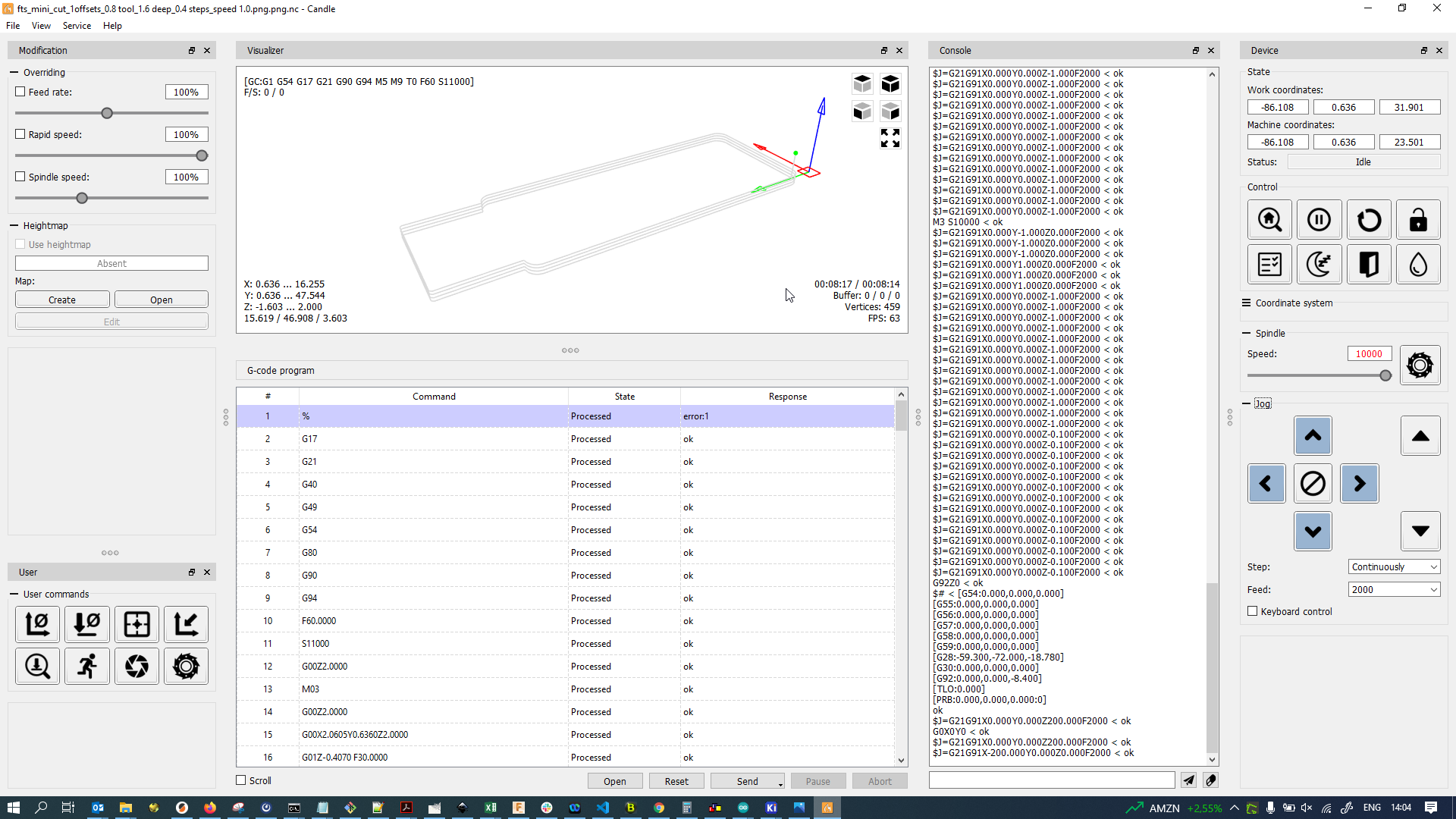
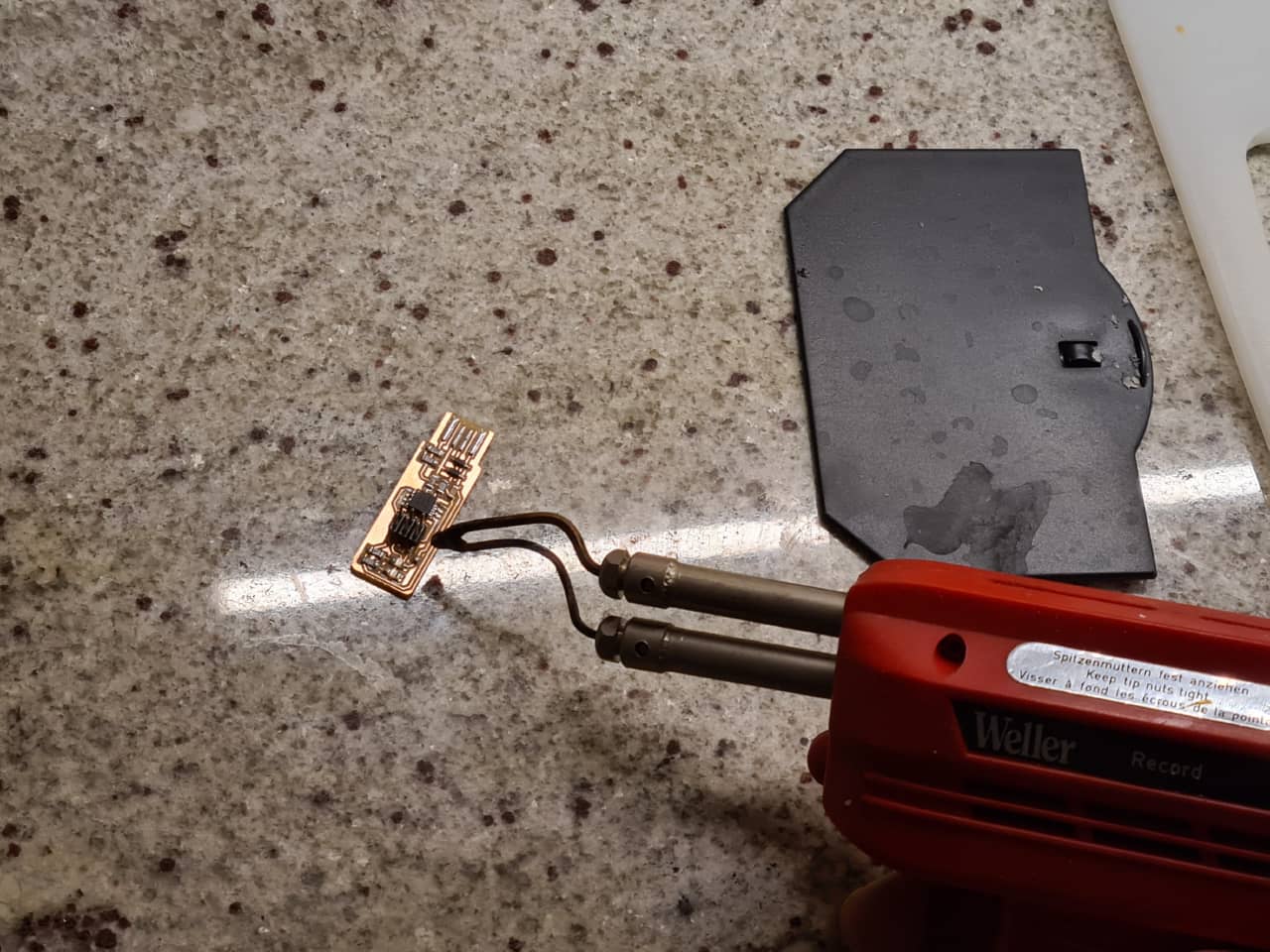
For making the ISP programmer I started by milling the board (Gcode prepared in Mods, milled on the Genmitsu 3018 PCB mill). This screenshot shows the board outline Gcode opened in Candle for milling with the Genmitsu PCB mill:
After milling, I started by soldering on the microcontroller (ATTiny85):
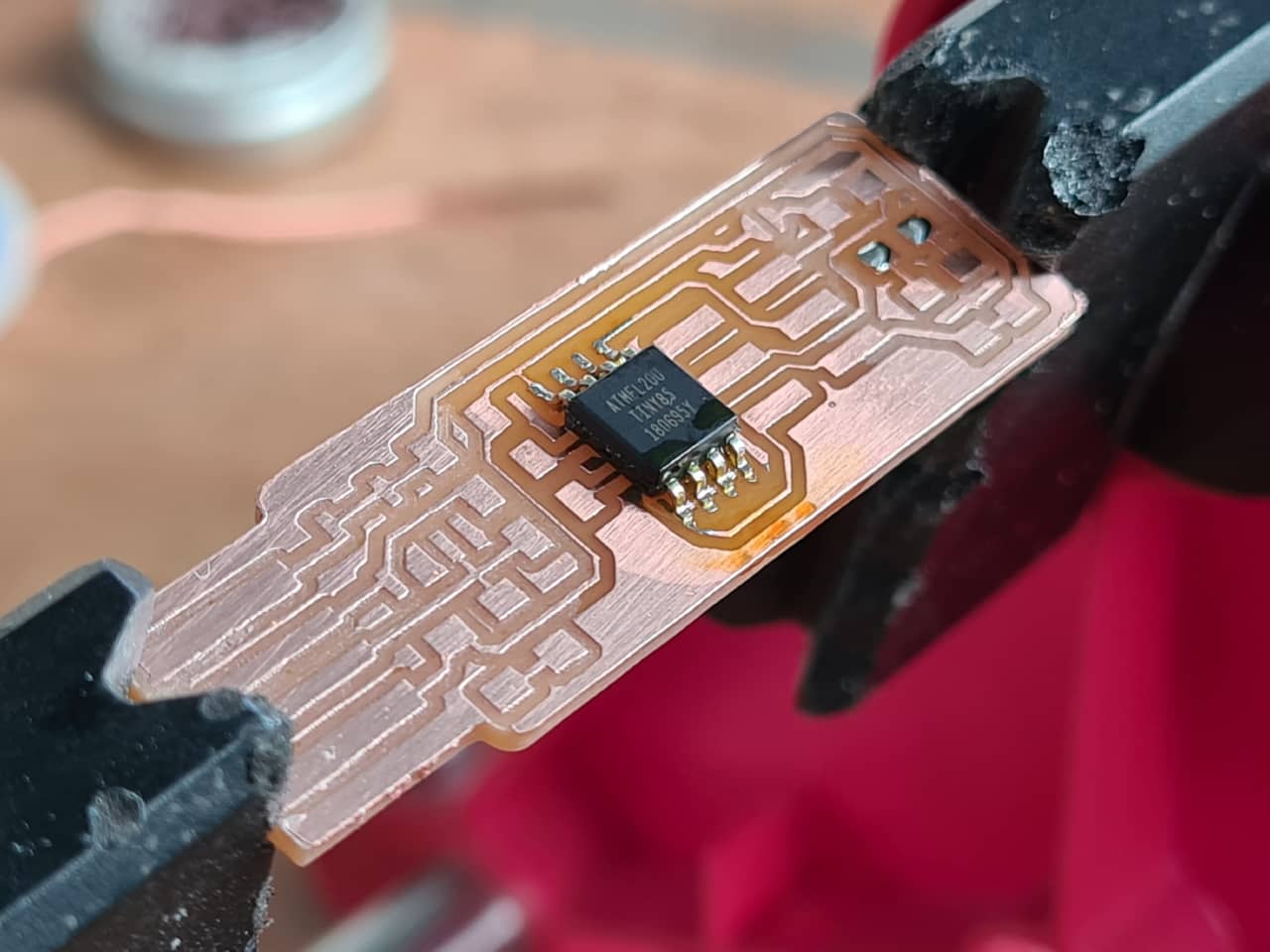
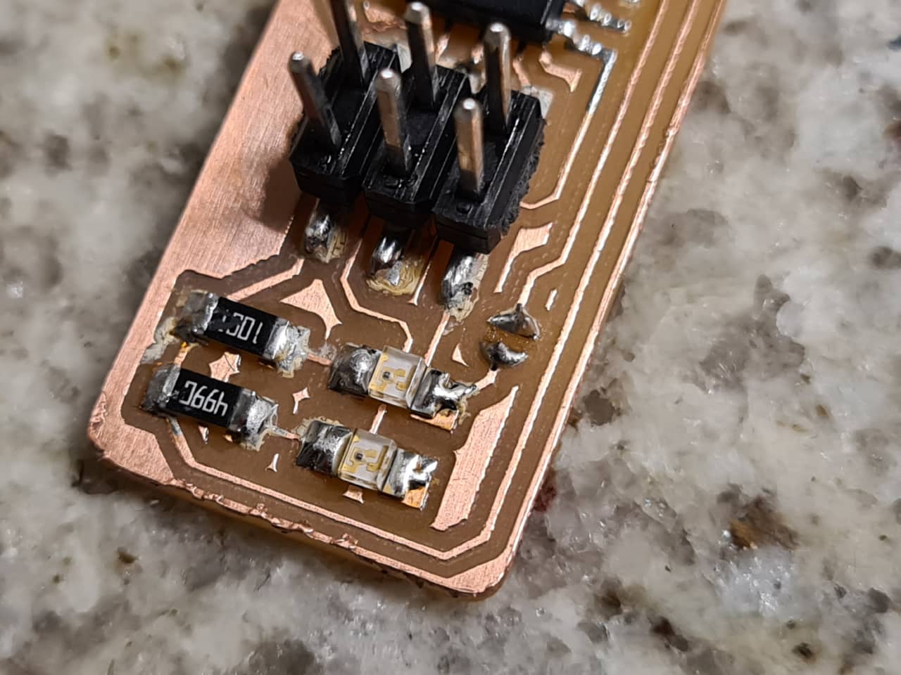
I then added resistors, LEDs and capacitor, …
… some more resistors and diodes and a helluvah flux. What a gunky mess:
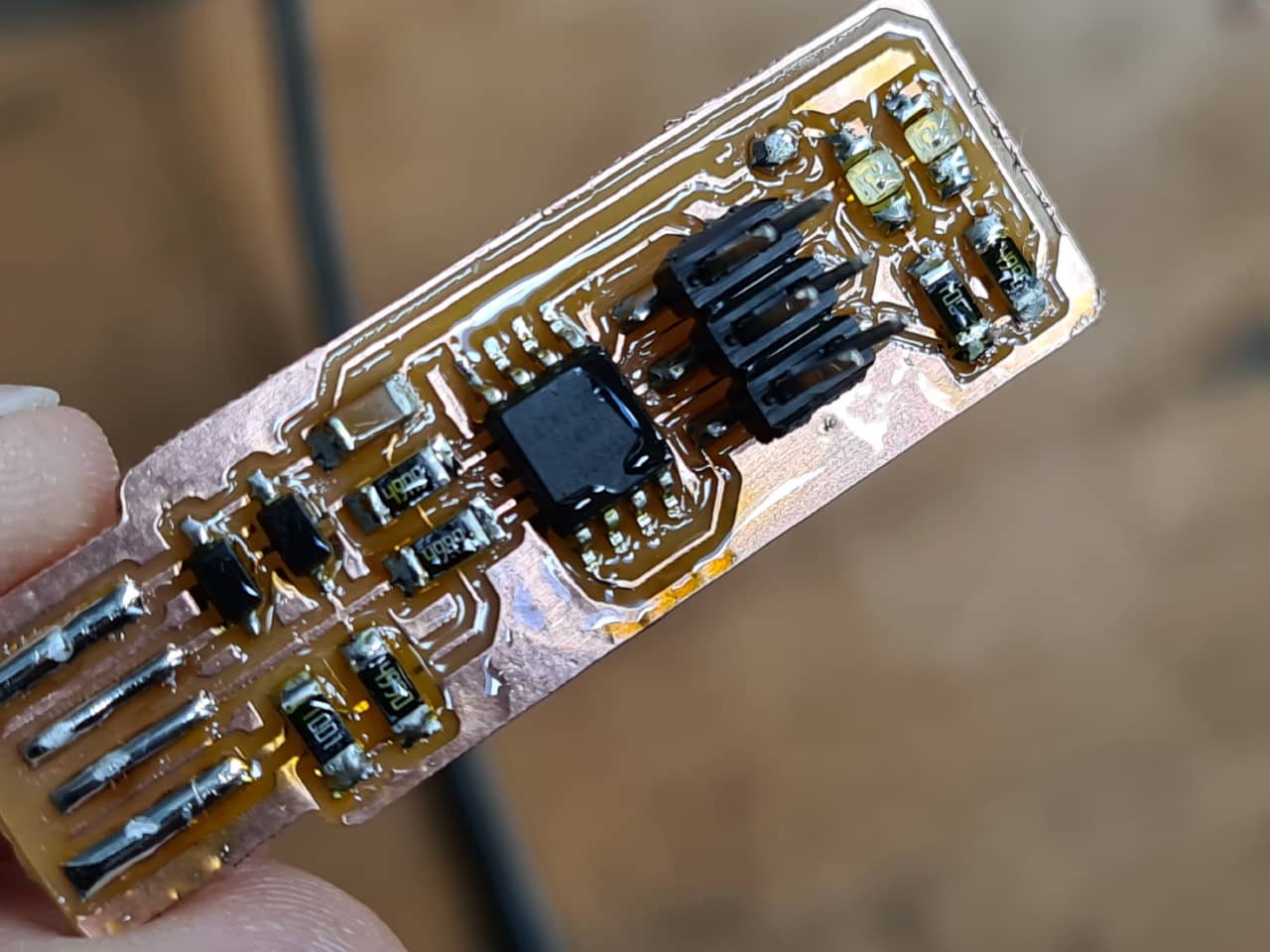
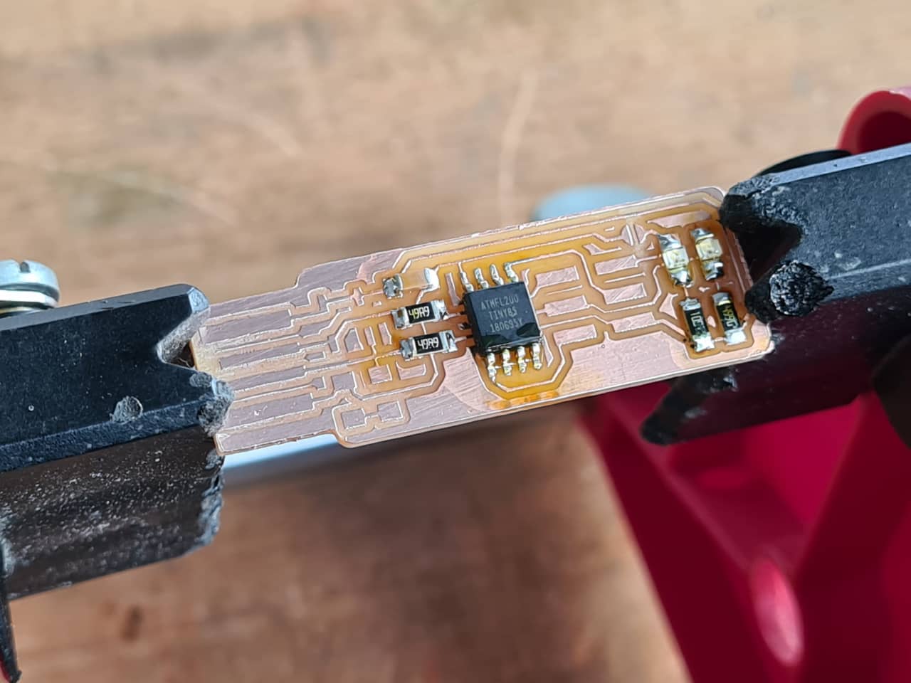
After washing the board in spirits (cheap Denatured Ethanol for a first wash, 99 % Isopropanol for a second wash) and drying, I measured for shorts and performed the smoke test - no smoke:
Who programs the programmers?
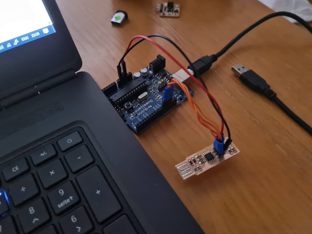
I then connected the Arduino Duemilanove to be used as an ISP programmer to burn the programmer firmware onto the ATTiny85:
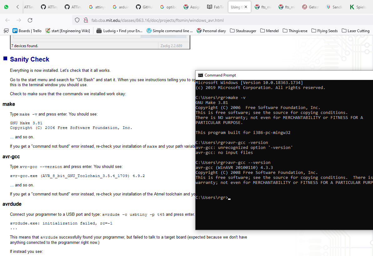
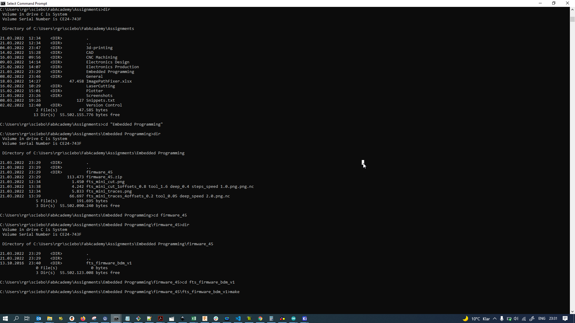
I didn’t have to set up the toolchain for compiling firmware before flashing it since all the tools were already installed (make, libgcc, avrdude). Here are the instructions for how to check for available software and the command line commands I executed to do so:
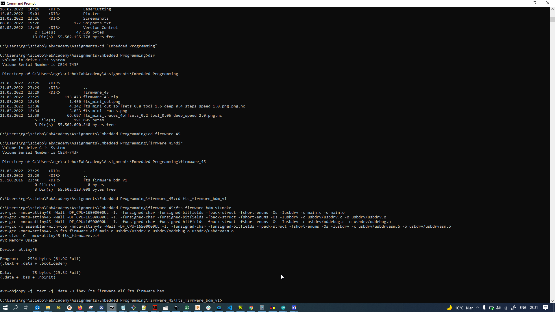
The firmware compiled without problems. Running the Make command to generate the firmware for the ATTiny45…
…and its output after finishing. All went well:
Since the FabTinyISP’s ATtiny85 does not have the code for acting as a programmer yet, we have to program it first to do so. I used the proven method of Arduino as ISP to burn the programmer code onto the FabTinyISP. Following the tutorial, for burning the firmware, we need to “update the Makefile for the type of programmer you’re going to use to program your board”. To find out which values to put in for when using the Arduino as ISP, I activated verbose console output in Arduino IDE and looked at what parameters avrdude was called with when uploading code using the Arduino as ISP as a programmer. In my case these were:
- programmer: stk500v1
- port: Arduino as ISP‘s COM port (this was COM22 for me, but could be any number for you or even something else when not on Windows)
- bitrate: 19200
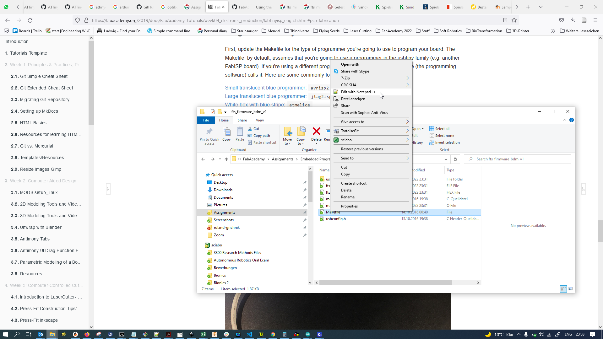
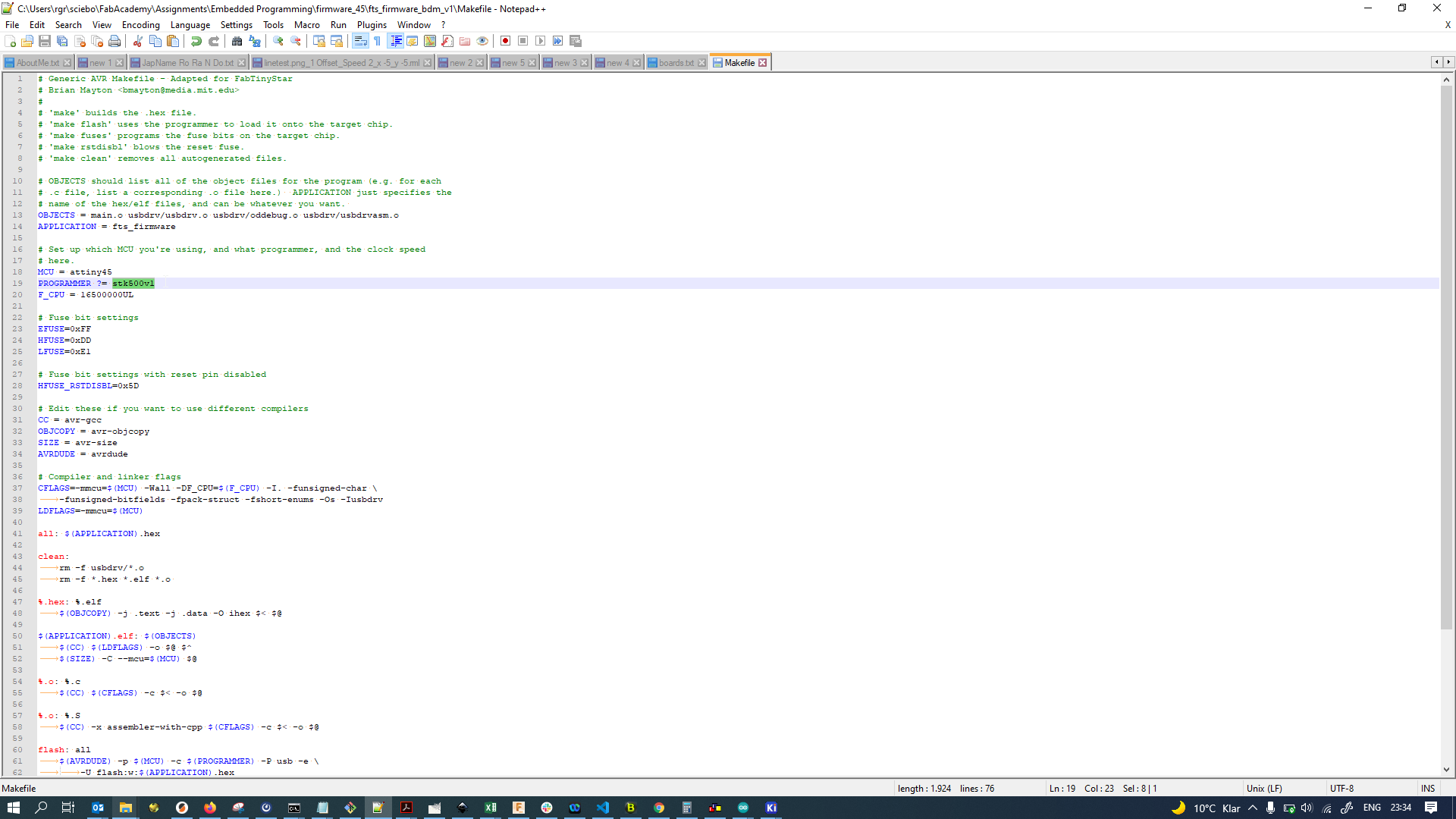
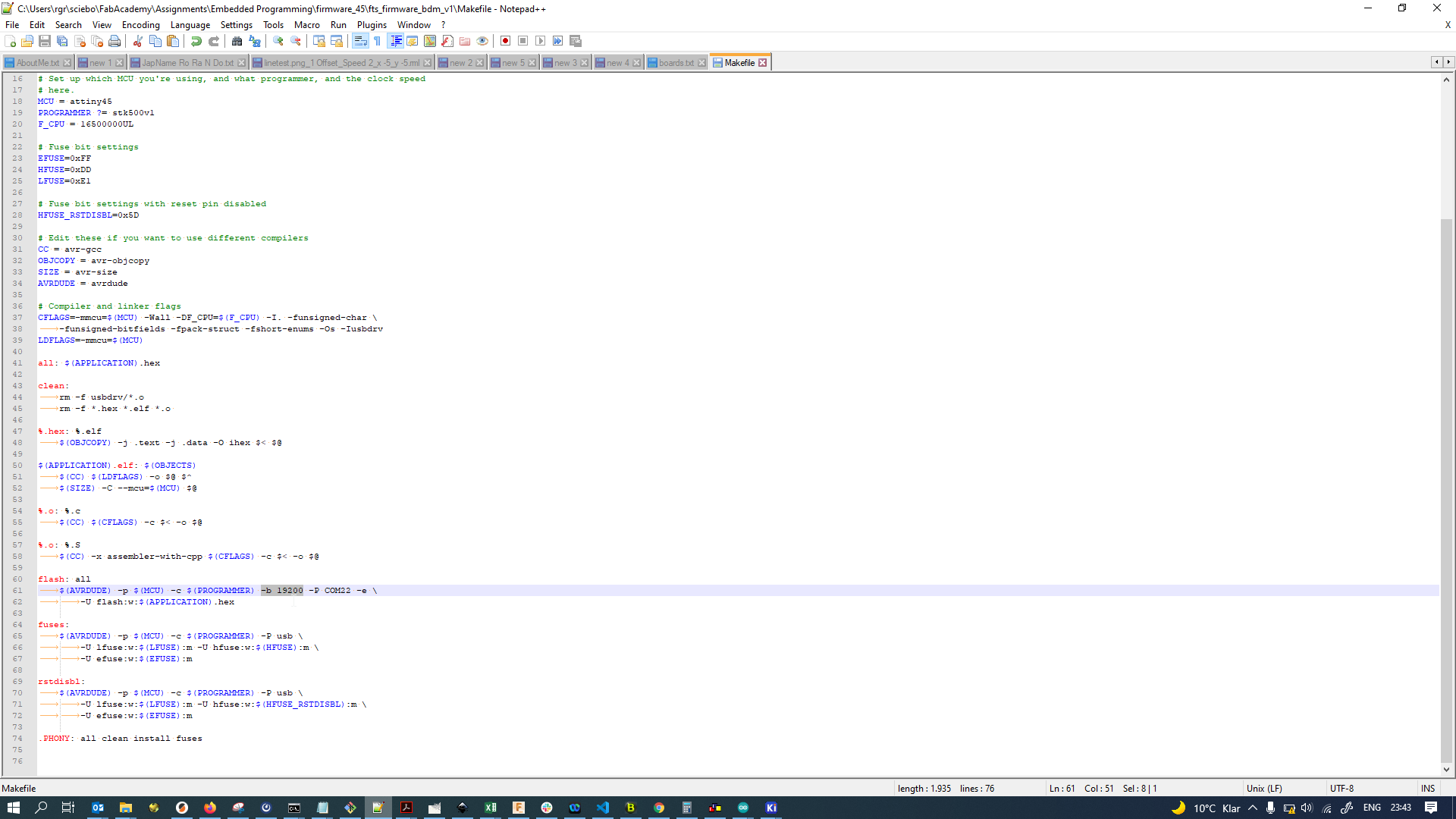
I edited the Makefile using Notepad++:
I needed to change the programmer to stk500v1…
and set the COM port to the Arduino Duemilanove’s COM port to allow flashing using the Arduino as ISP solution:

When trying to flash the firmware first, the programmer couldn’t manage to establish a connection:
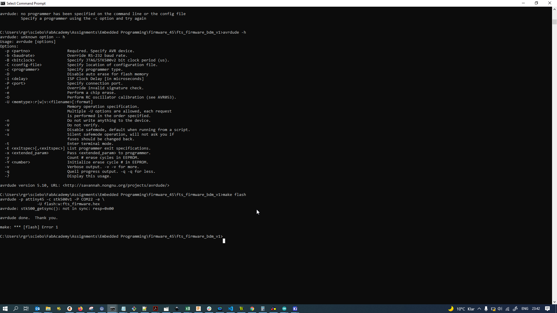
Turns out that when using the Arduino as ISP, the communication rate should be lowered to allow for some breathing room. I changed the baudrate for communication by adding another parameter to the Make commands in the Makefile:
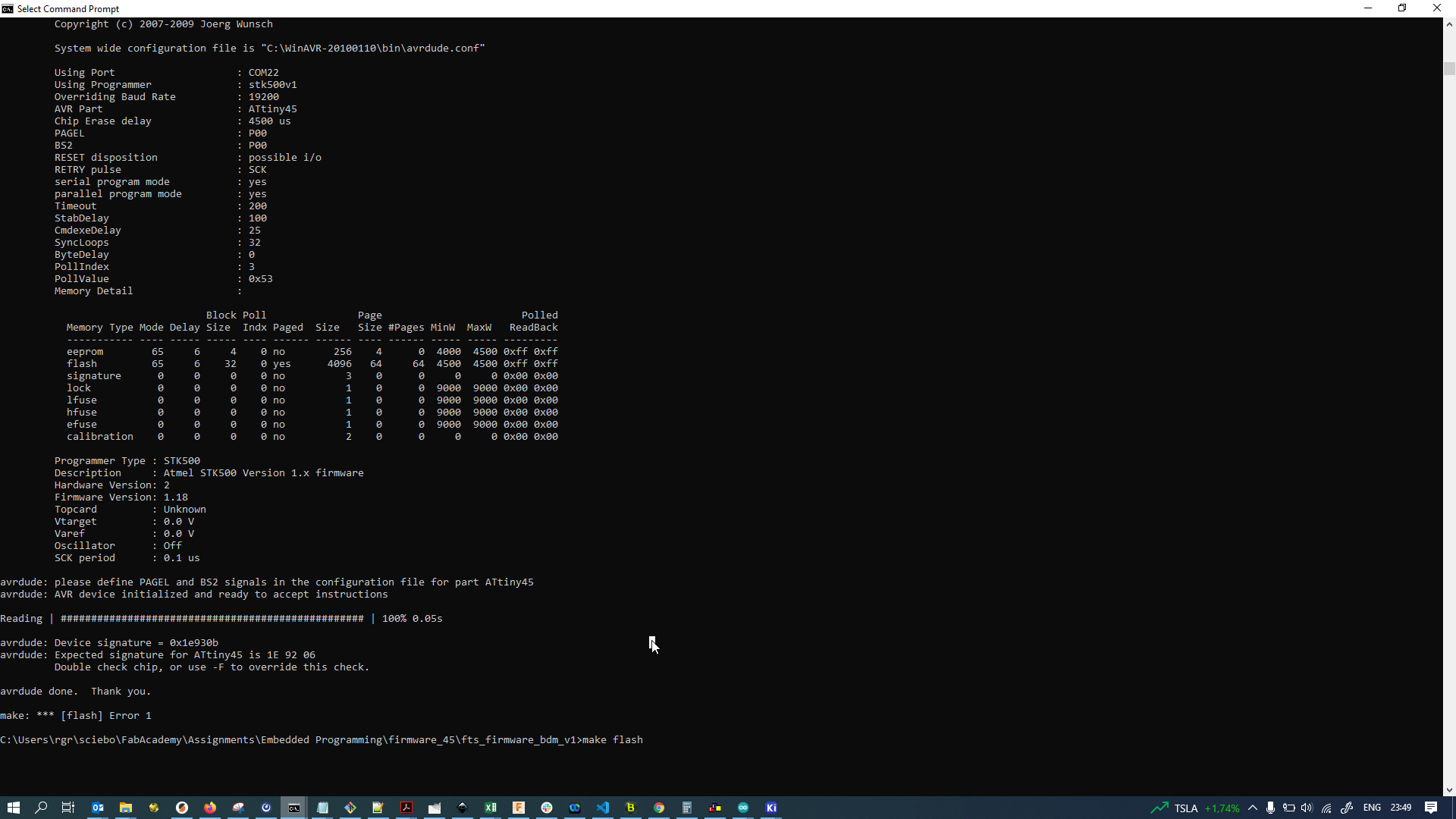
After changing the makefile as described, running the make command for flashing the firmware did actually work, but reported a device mismatch… D’oh - avrdude was expecting to see an ATTiny45:
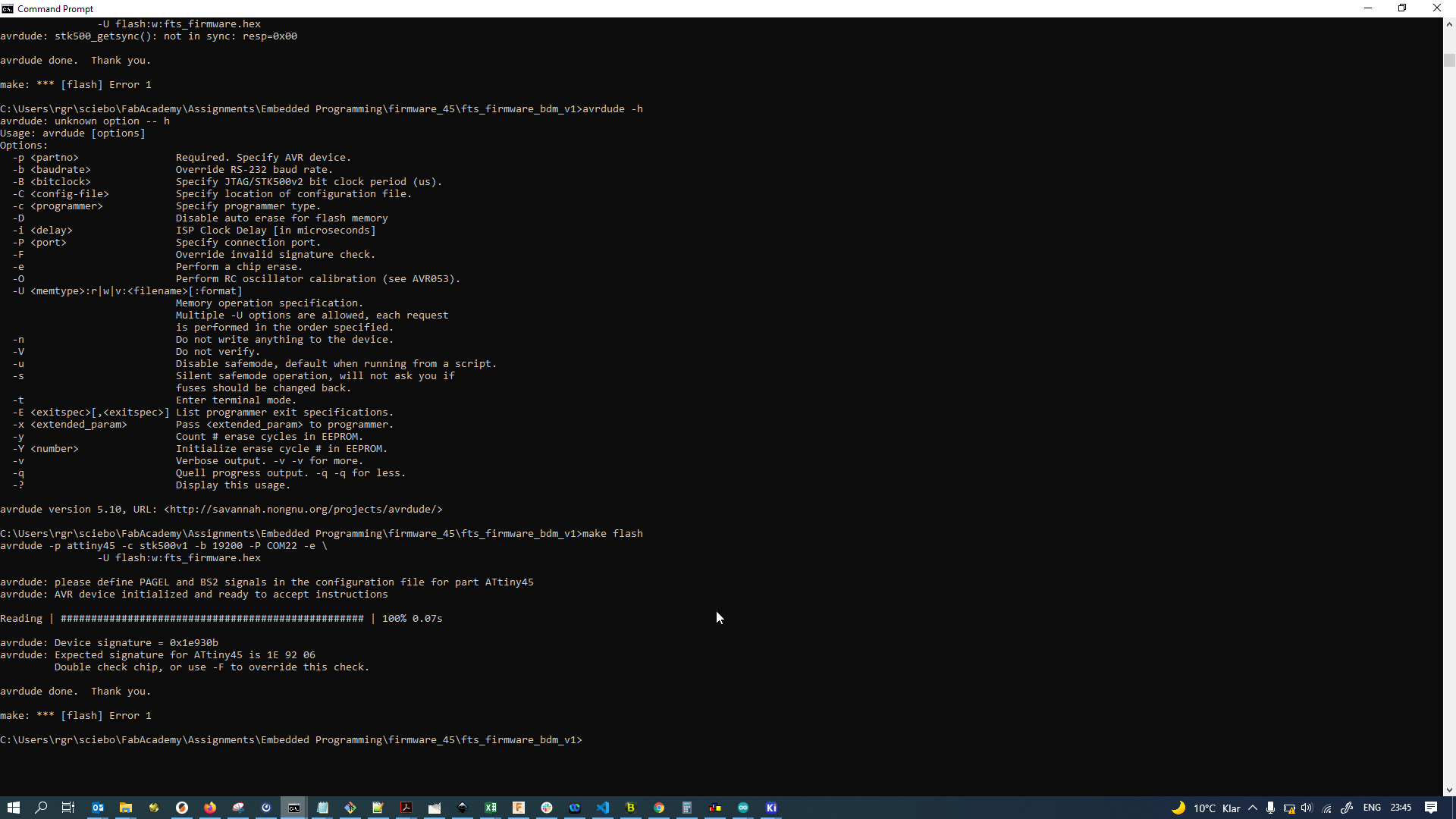
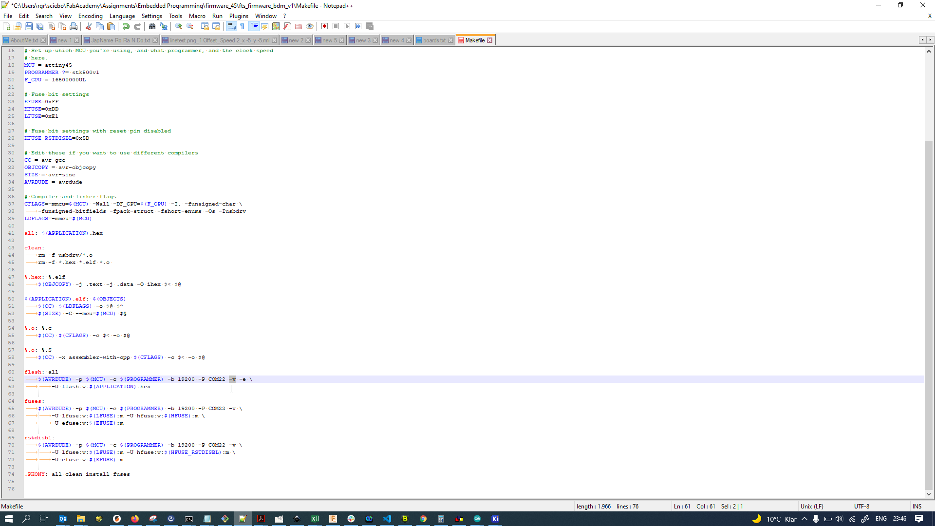
I added verbose output option to the Makefile commands so I would have more information/feedback from avrdude:
Here is the failed Make flash command again with verbose output. Not much new info, still, just a device mismatch. D’uh…
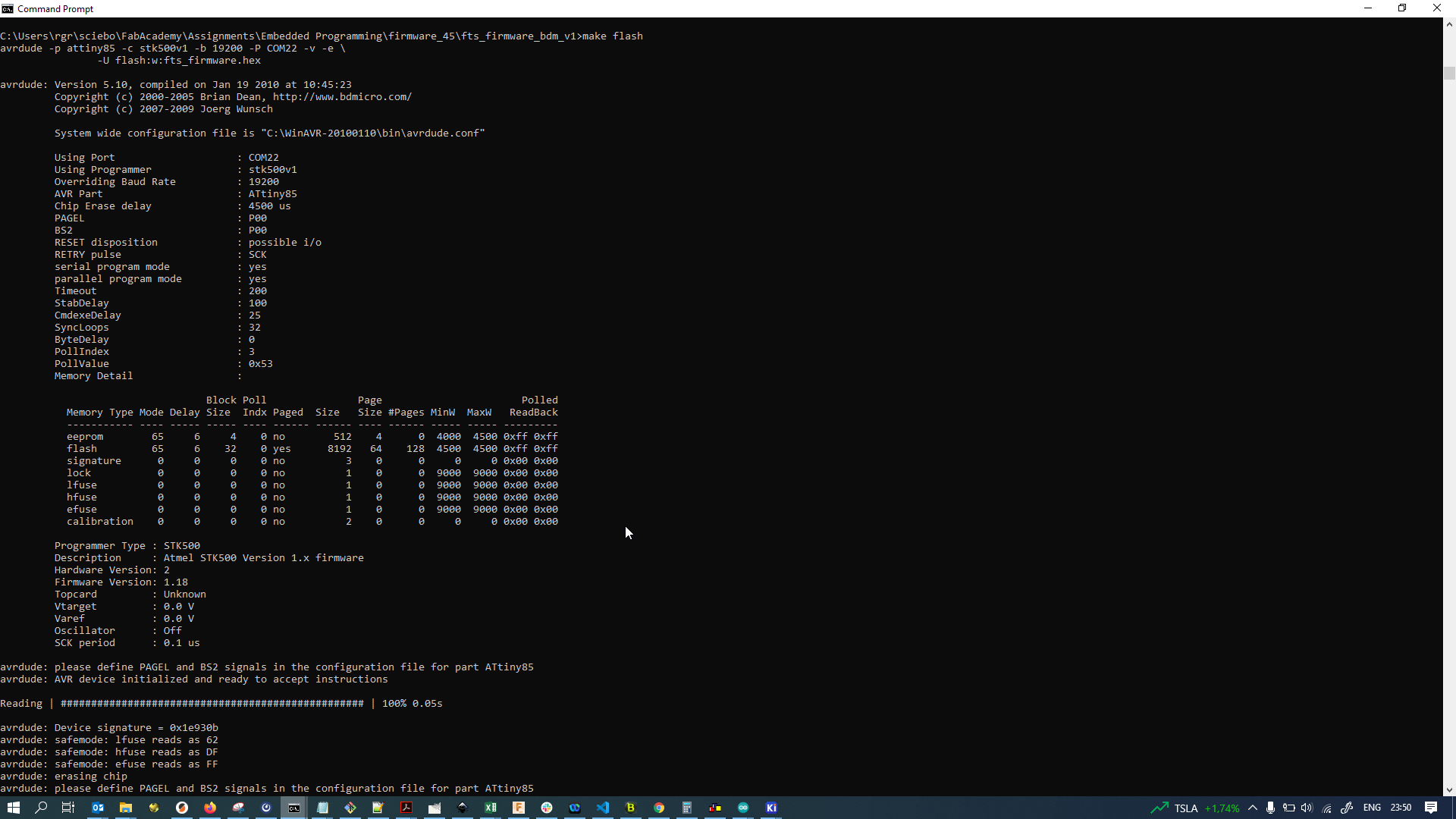
…I had forgotten that instead of the ATTiny45 the firmware and makefile was provided for, I used an ATTiny85. So I changed the chip target for the Make file to ATTiny85, as that is what I had installed on my board:

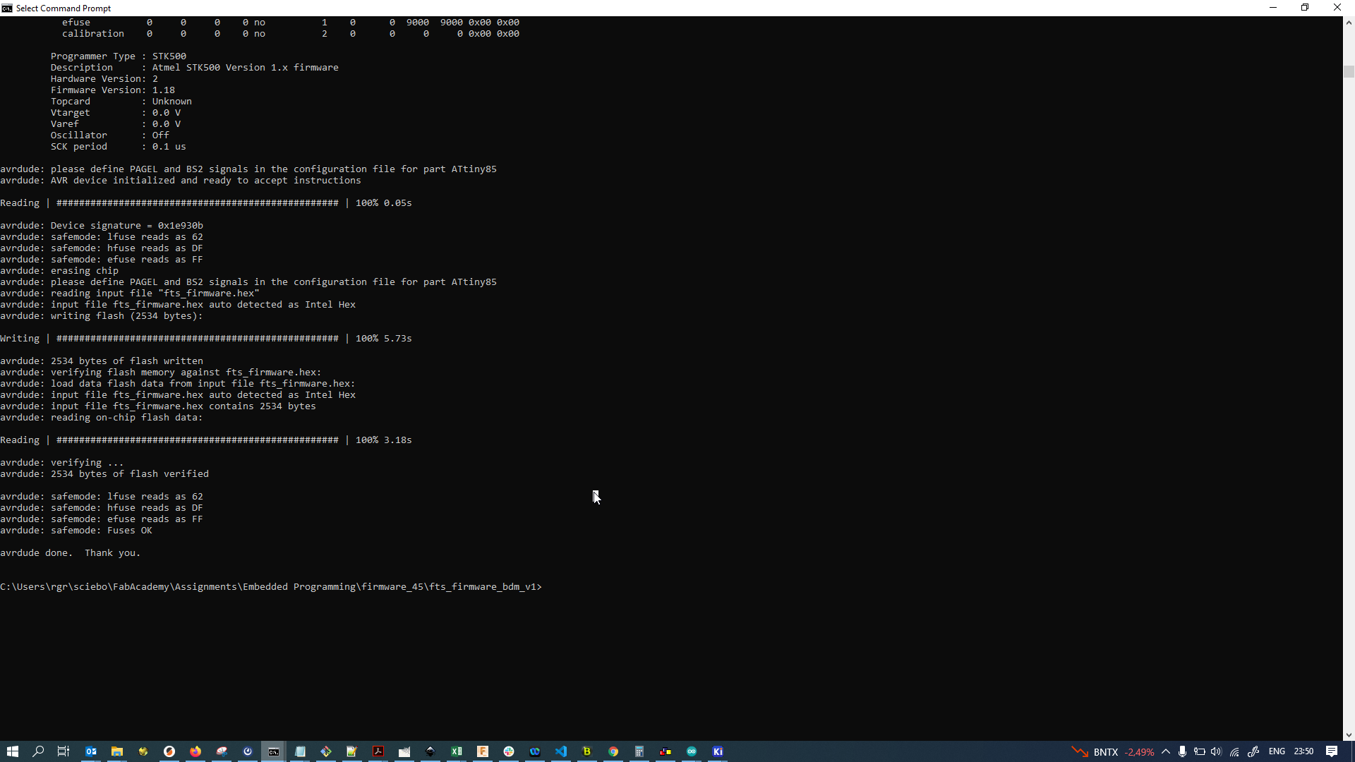
After that, the Make flash command finished successfully and compiled…
…as well as flashed the firmware successfully to my board;
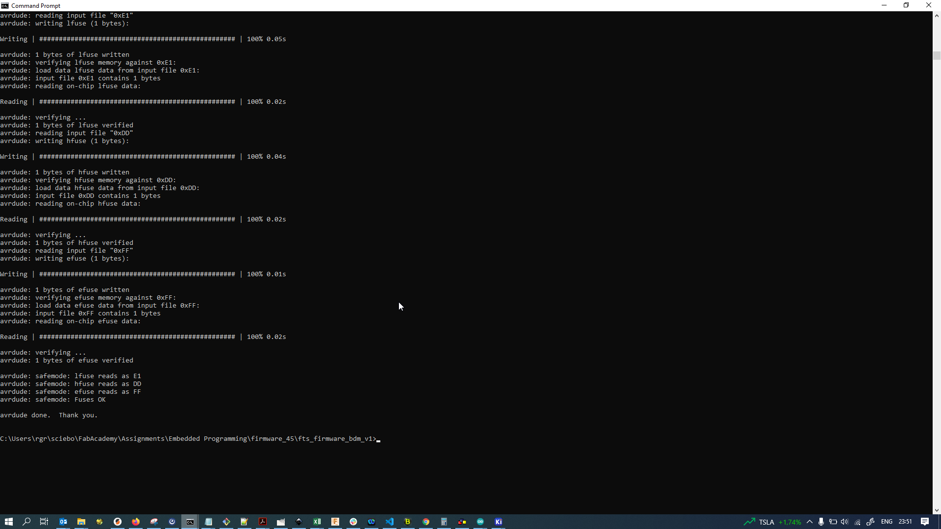
The Make fuses command to write the fuses…
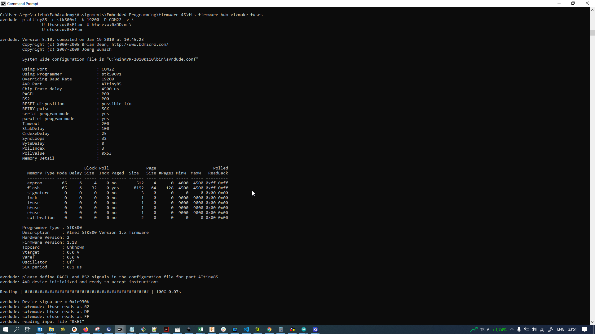
…also performed successfully without problems:
Here’s the important changes to the makefile again, the final makefile is also in the downloadable files (replace COM22 by whatever your Arduino as ISP‘s port is):
...
MCU = attiny85
PROGRAMMER ?= stk500v1
...
...
...
flash: all
    $(AVRDUDE) -p $(MCU) -c $(PROGRAMMER) -b 19200 -P COM22 -v -e \
        -U flash:w:$(APPLICATION).hex

fuses:
    $(AVRDUDE) -p $(MCU) -c $(PROGRAMMER) -b 19200 -P COM22 -v \
        -U lfuse:w:$(LFUSE):m -U hfuse:w:$(HFUSE):m \
        -U efuse:w:$(EFUSE):m

rstdisbl:
    $(AVRDUDE) -p $(MCU) -c $(PROGRAMMER) -b 19200 -P COM22 -v \
        -U lfuse:w:$(LFUSE):m -U hfuse:w:$(HFUSE_RSTDISBL):m \
        -U efuse:w:$(EFUSE):m
...
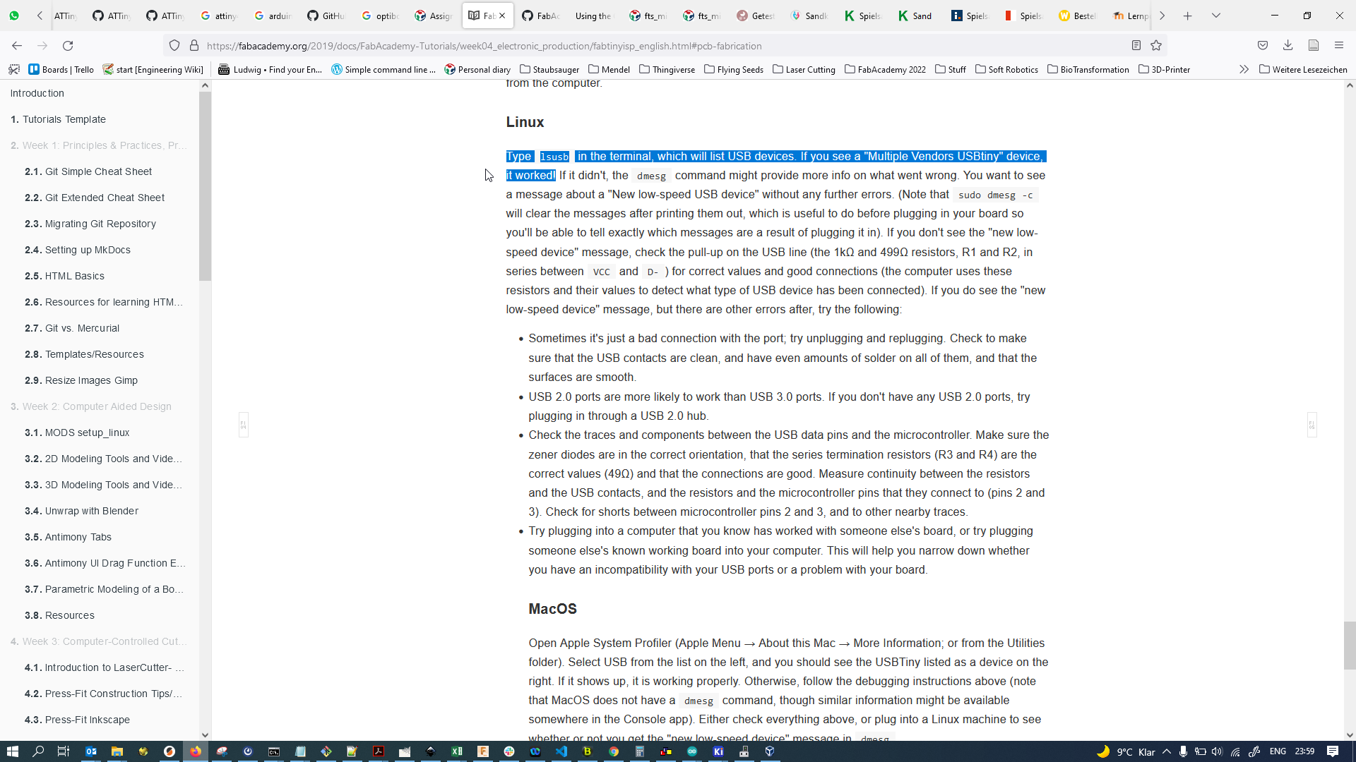
Validating USB functionality
To make sure the board worked fine, I followed the tips to check for USB functionality in the tutorial, as per these instructions:
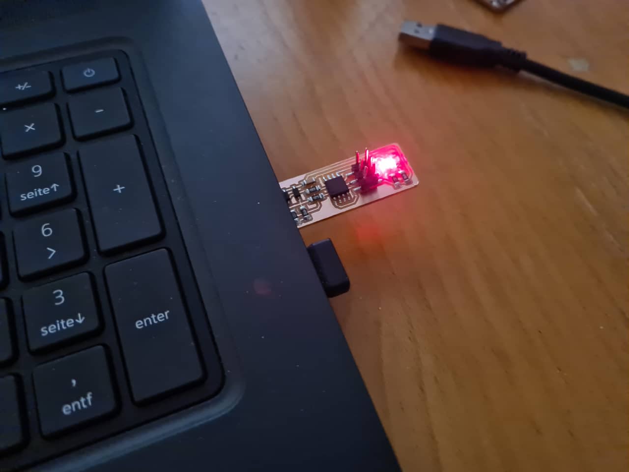
First things first, the device enumerated as a USB device under Windows 10, as showing in the little popup in the bottom right here:
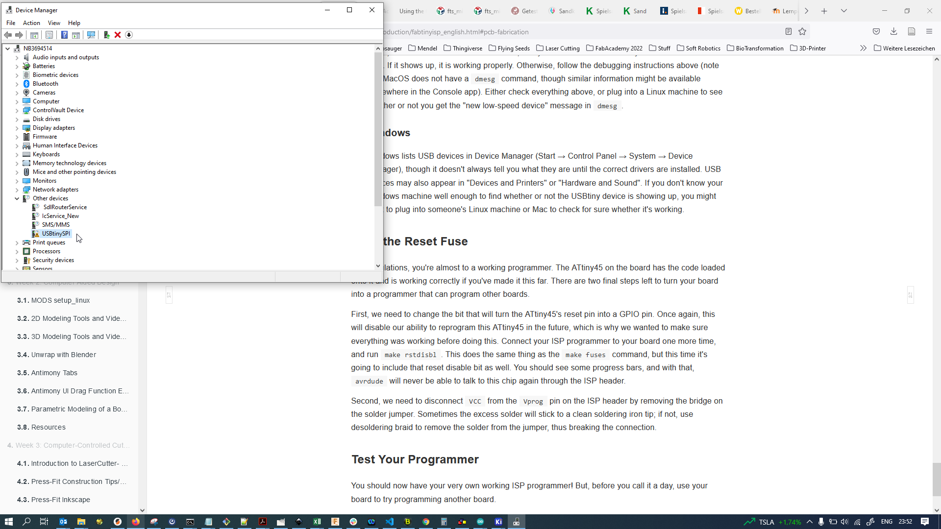
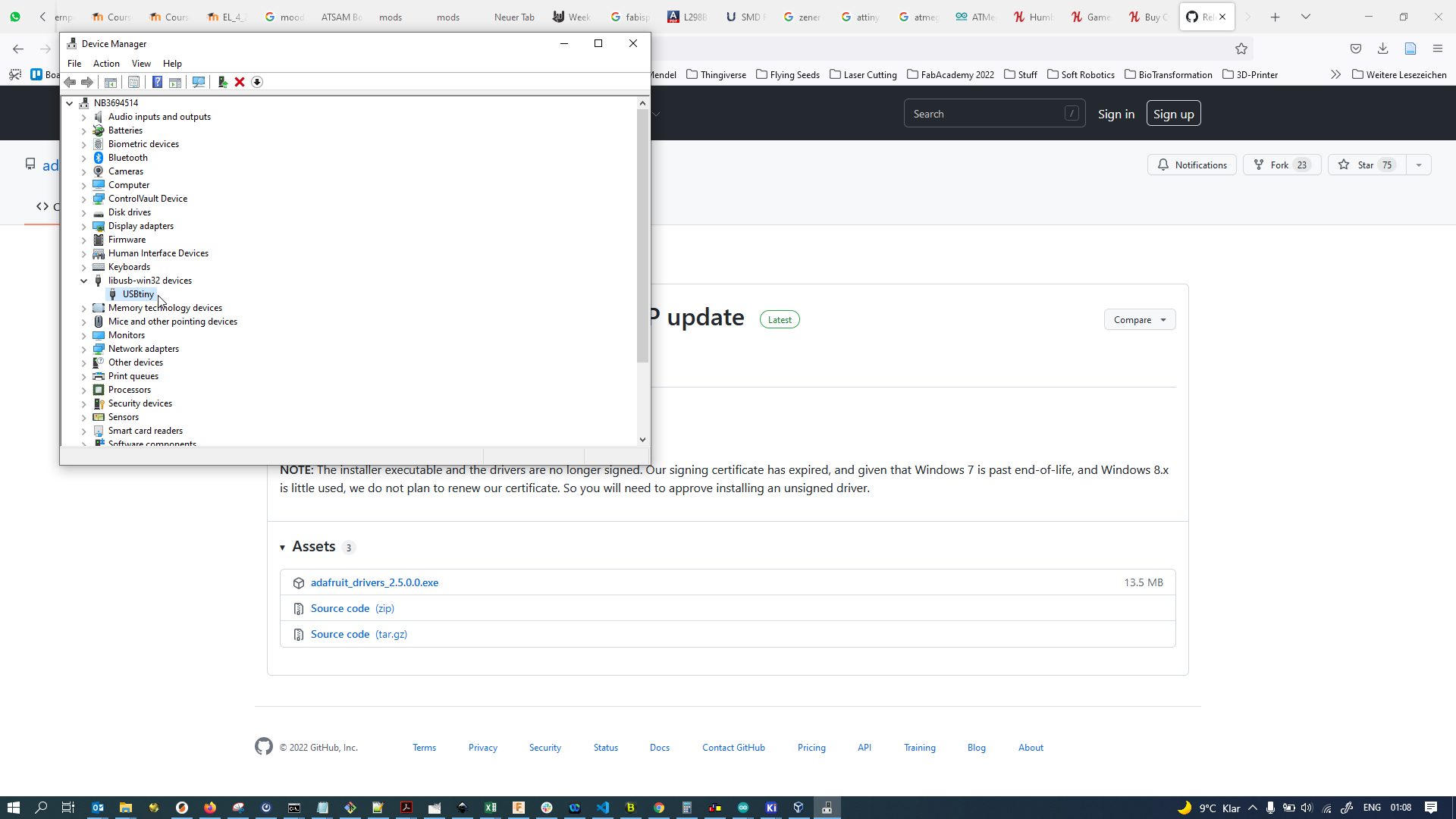
The board did turn up in my Windows machine’s device manager, yet as a USBTinySPI (not ISP as expected).:
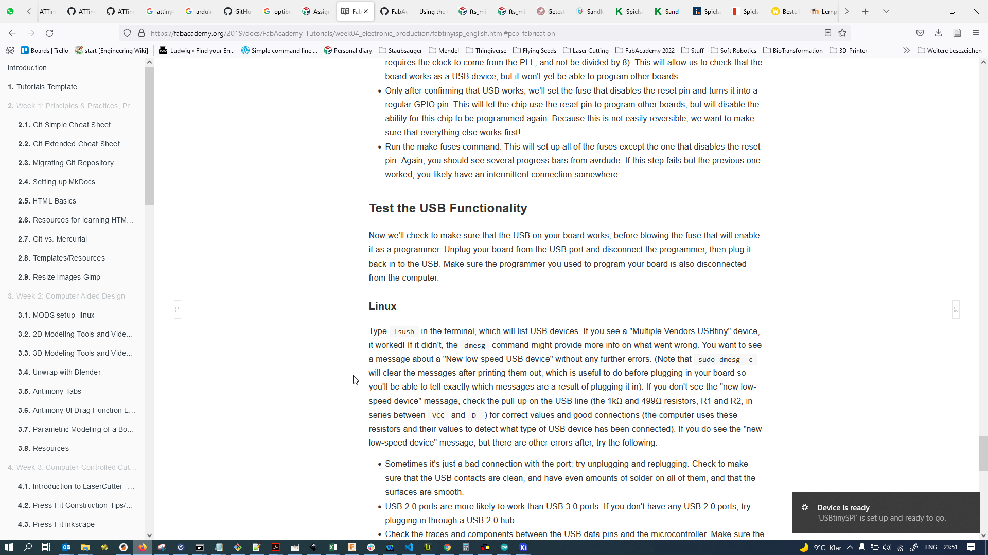
The entry in device manager also had a warning icon, meaning drivers might not be installed for the device. To make doubly sure, I also fired up a Ubuntu Virtual Machine and gave it access to the USB so I could check the attached devices using lsusb as described in the instructions.
After forwarding the USB device into the Virtual Machine…
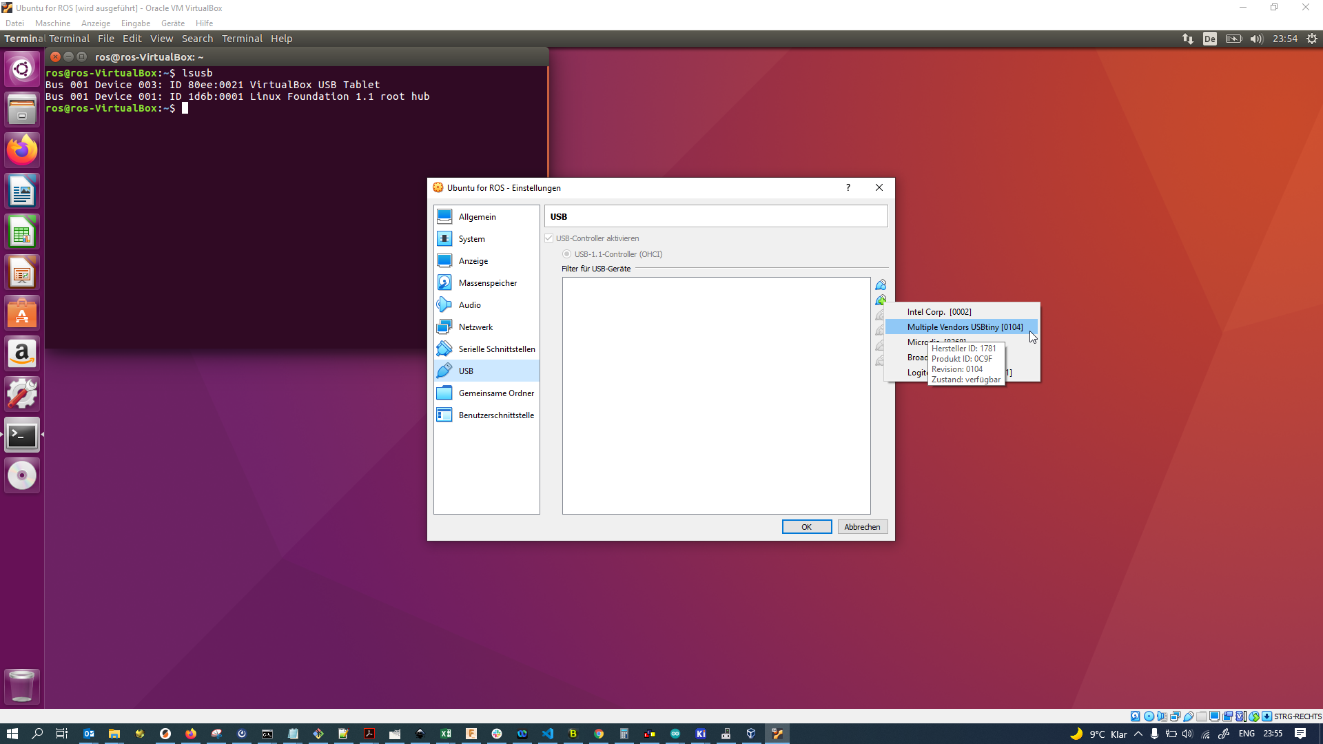
I could then find the device in the Terminal using the lsusb command, producing the expected output:
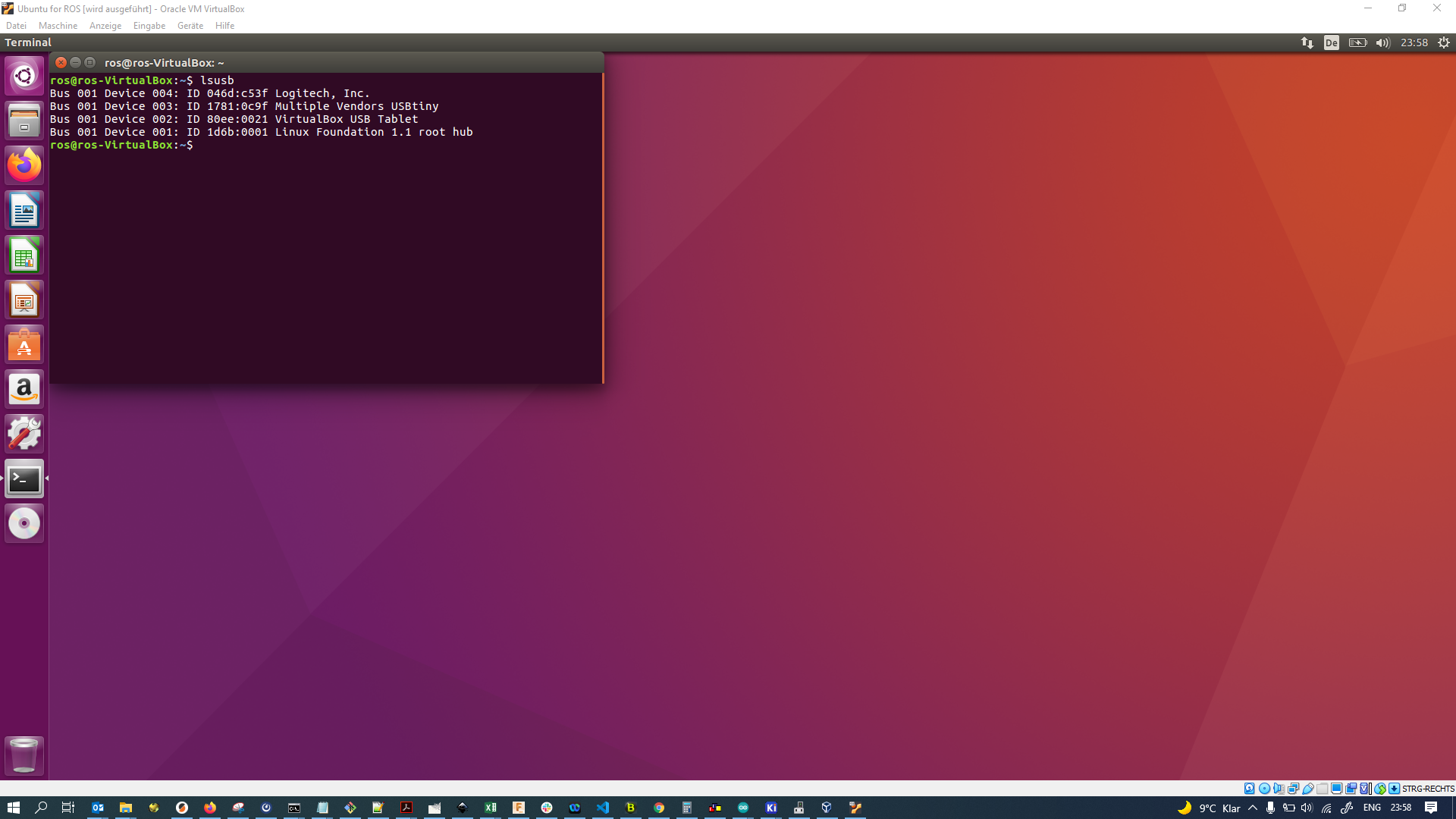
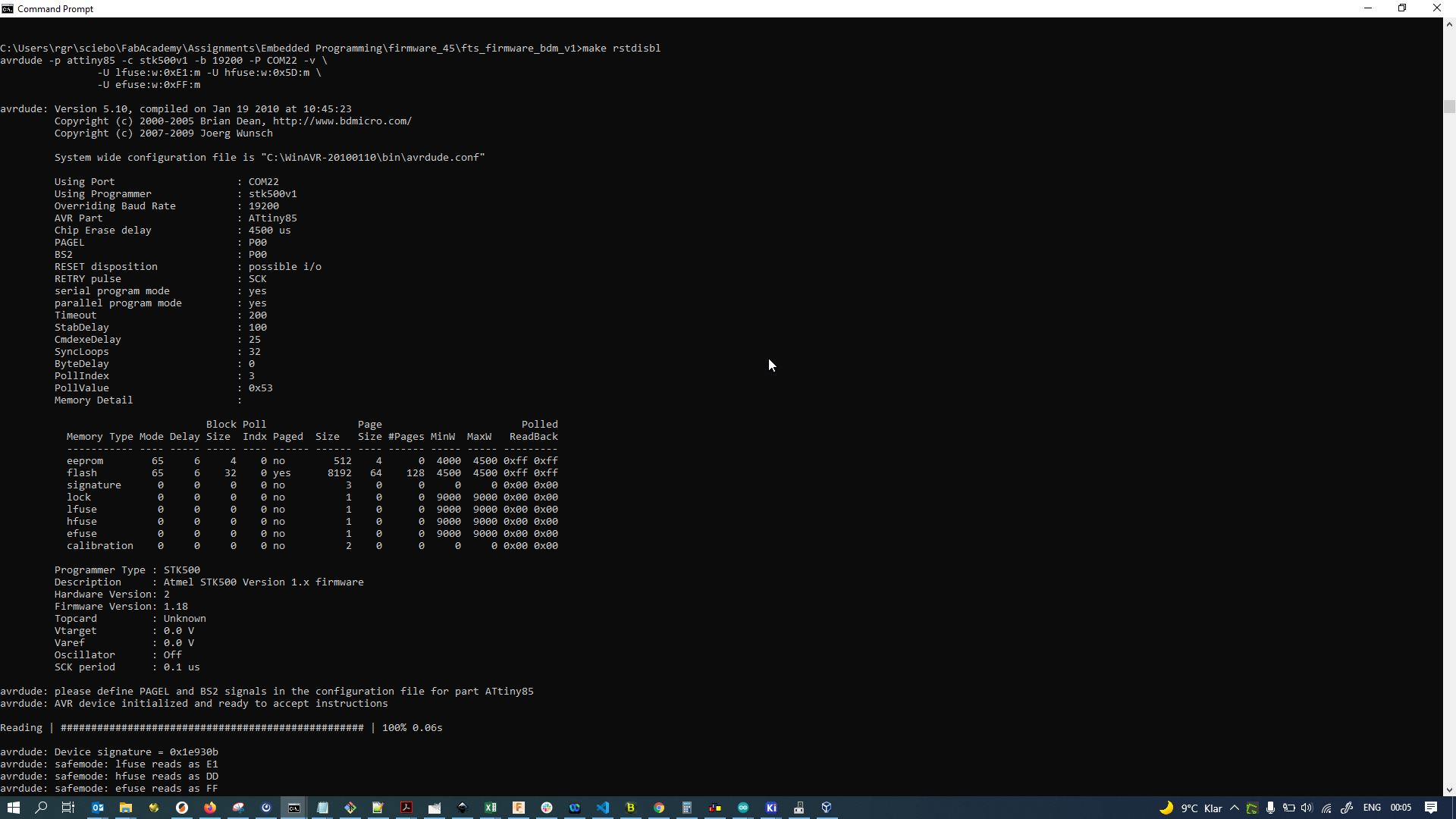
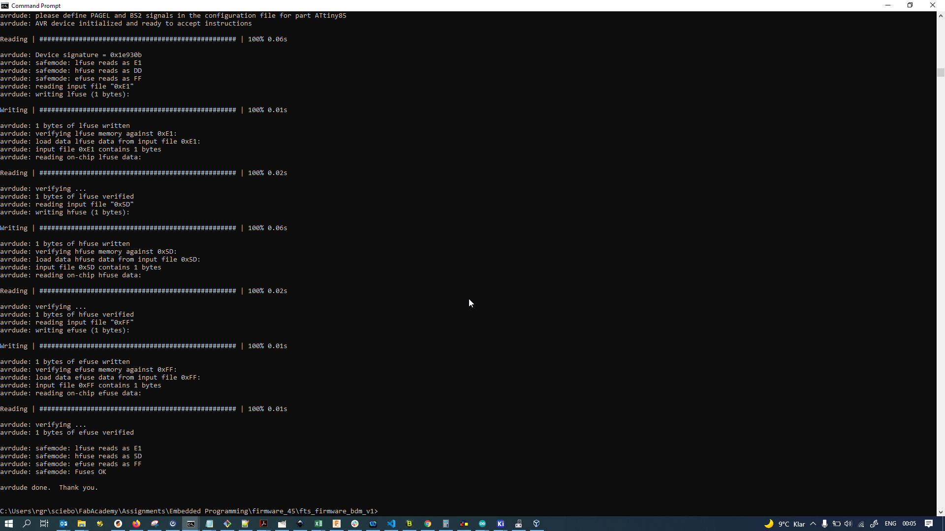
Since this turned up the exact result as described (showing “Multiple Vendors USBtiny” in the list of USB devices), I was sure it would work fine in the end. I went on and blew the “reset disable” fuse as per the instructions (by running the Make rstdisbl command), meaning the programmee could now not be programmed via ISP anymore:
This also finished without problems:
Finishing touches
As it was late and I was home and couldn’t find my soldering iron in the recent move’s boxes, I used a skookum soldering gun to remove the solder bridge …
… like a boss:
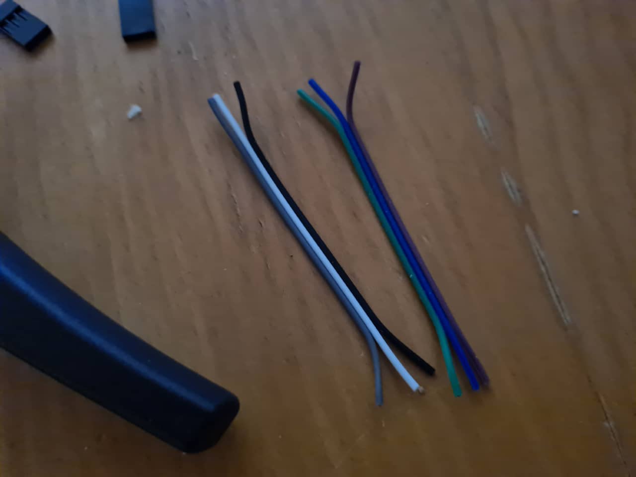
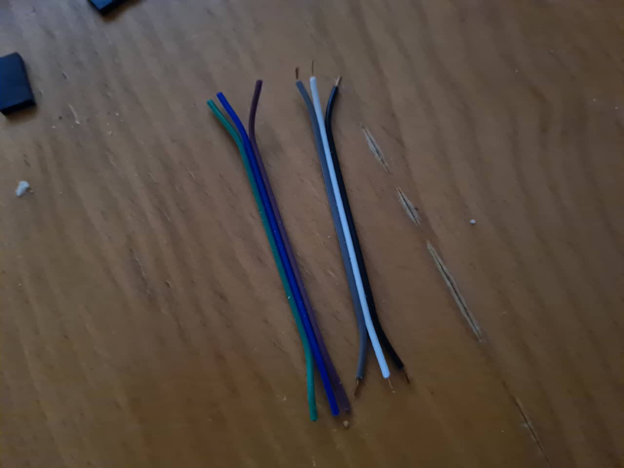
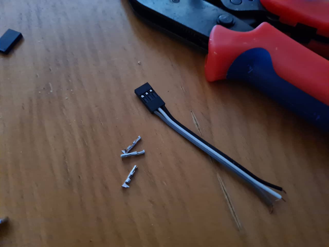
I then went on to make an ISP cable (or rather two 1x3 female jumper cables) using crimps:
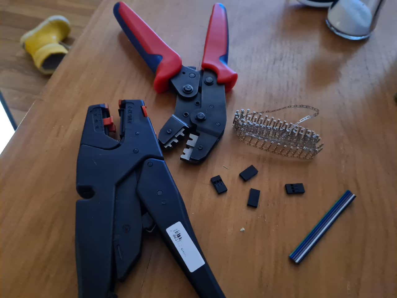
To start out, I lengthened off two lengths of ribbon cable, …
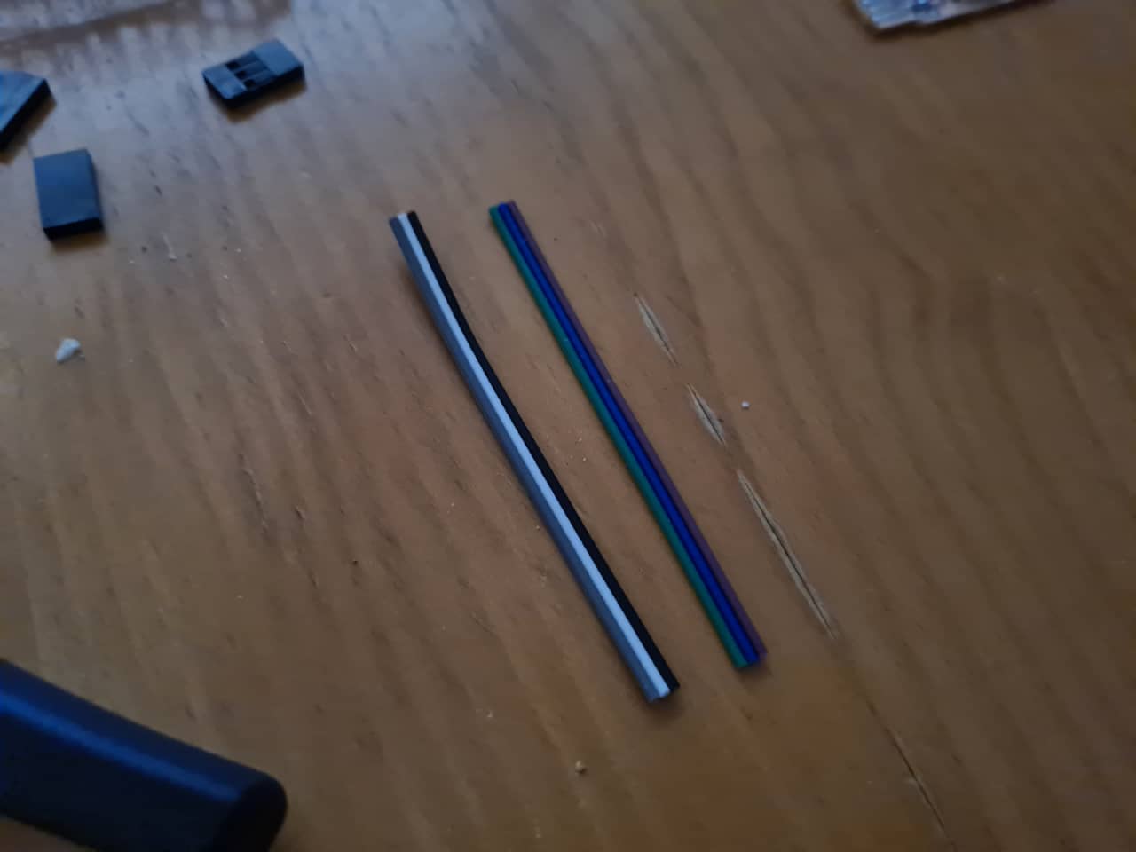
… fanned out the ends, …
… stripped them …
… and crimped on female connectors:
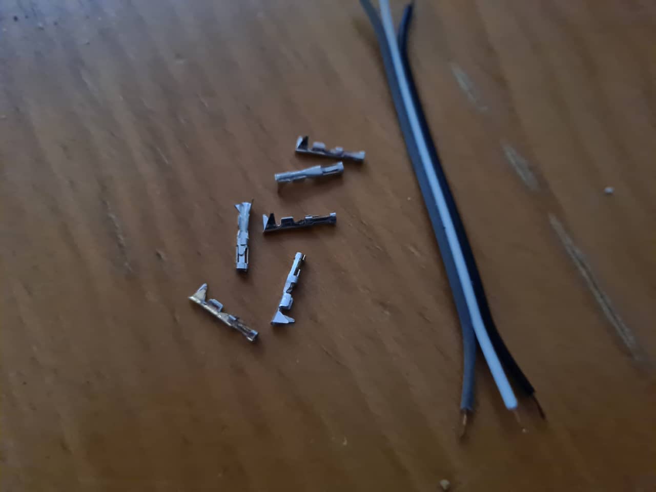
Here, the first crimps are already on …
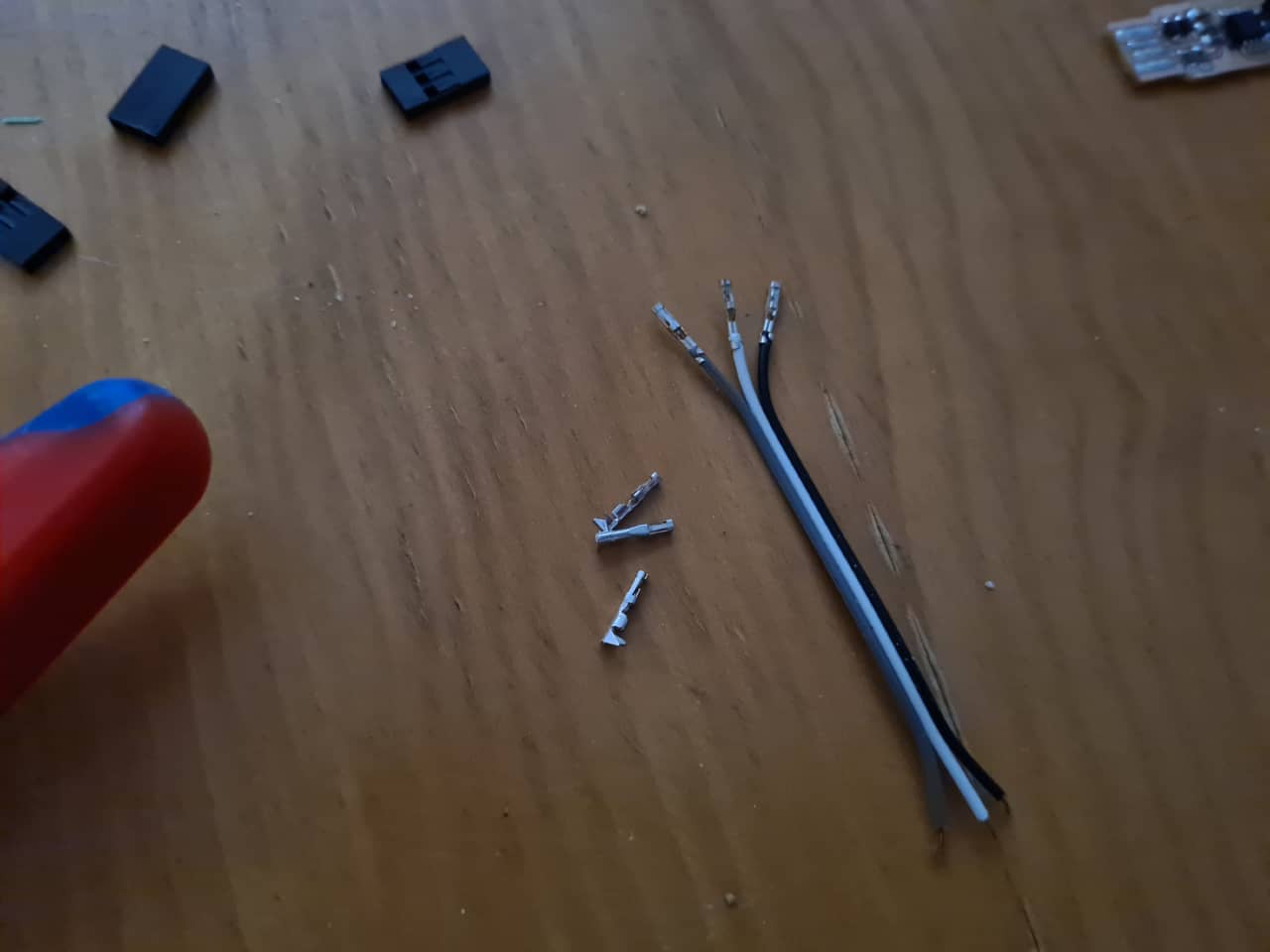
… and ready to be inserted into the housing:
Ready for Testing
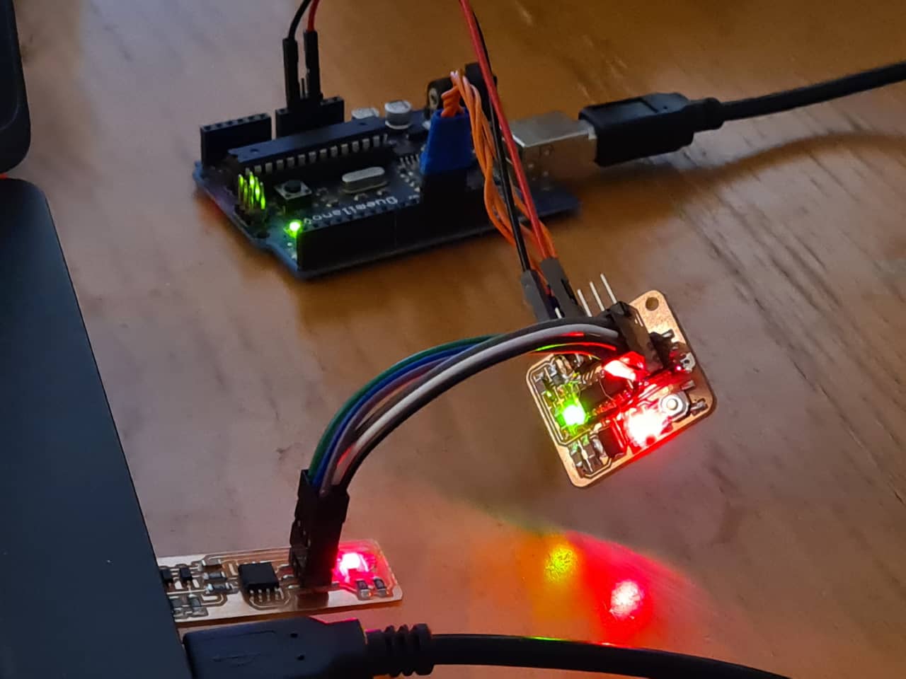
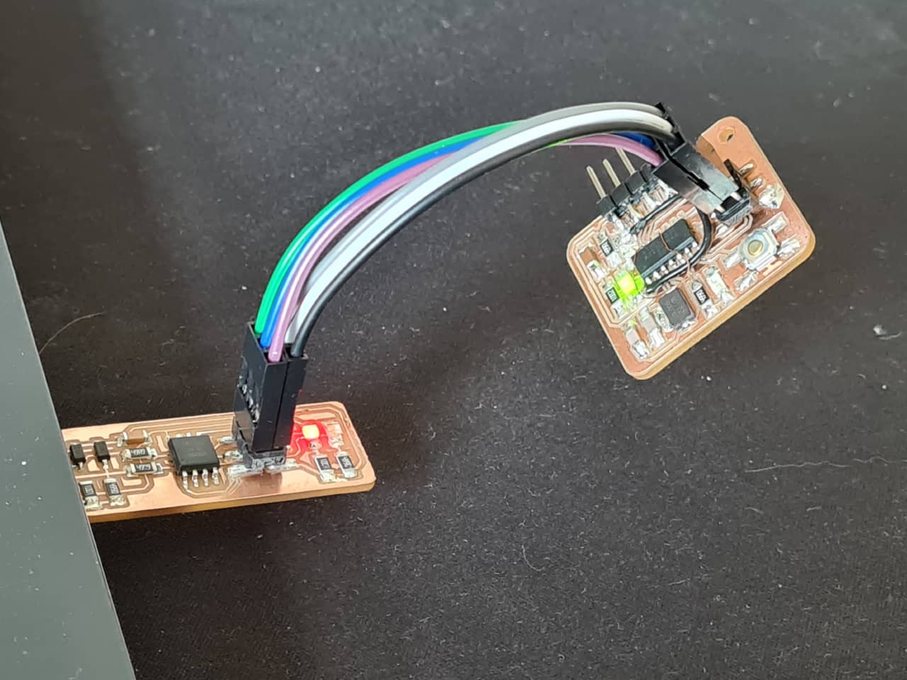
Using the two 1x3 jumpers, I connected the programmer’s ISP header to the programmee’s ISP header:
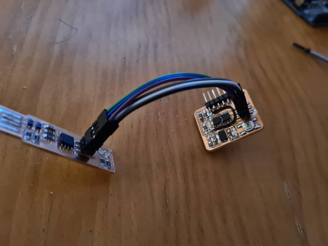
As I had removed the solder bridge earlier (which I will rectify later, again), I needed to power the programmee separately, in this case using two power jumpers from the Arduino Duemilanove (notice the ISP jumper is not connected to anything). I tested the programmer …
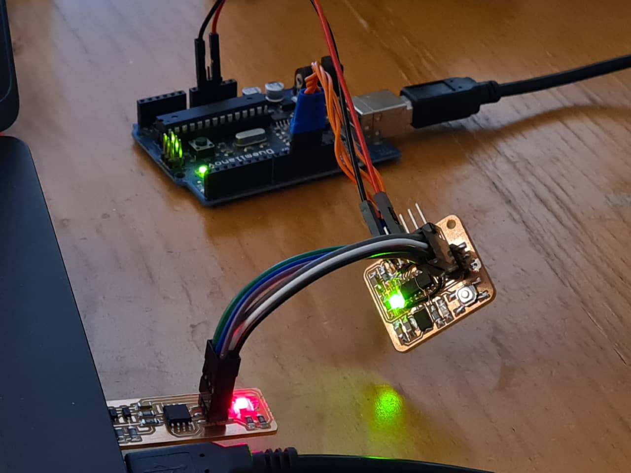
… but initially it did not work. When asking to program from the Arduino IDE, the IDE simply could not find the attached USB programmer. I decided to investigate the yellow triangle/missing driver situation and quickly landed at Adafruit’s driver download page, where I downloaded the driver for the usbtinyisp. After installation, the yellow triangle had vanished and the board was properly recognized.
Here’s the FabTinyISP showing up in Windows Device Manager after fixing the drivers from the Adafruit webpage…
Trying the programming from Arduino IDE again, it worked just fine, here showing first programming success, programming my ATTiny 44 echo board using my FabTinyISP:
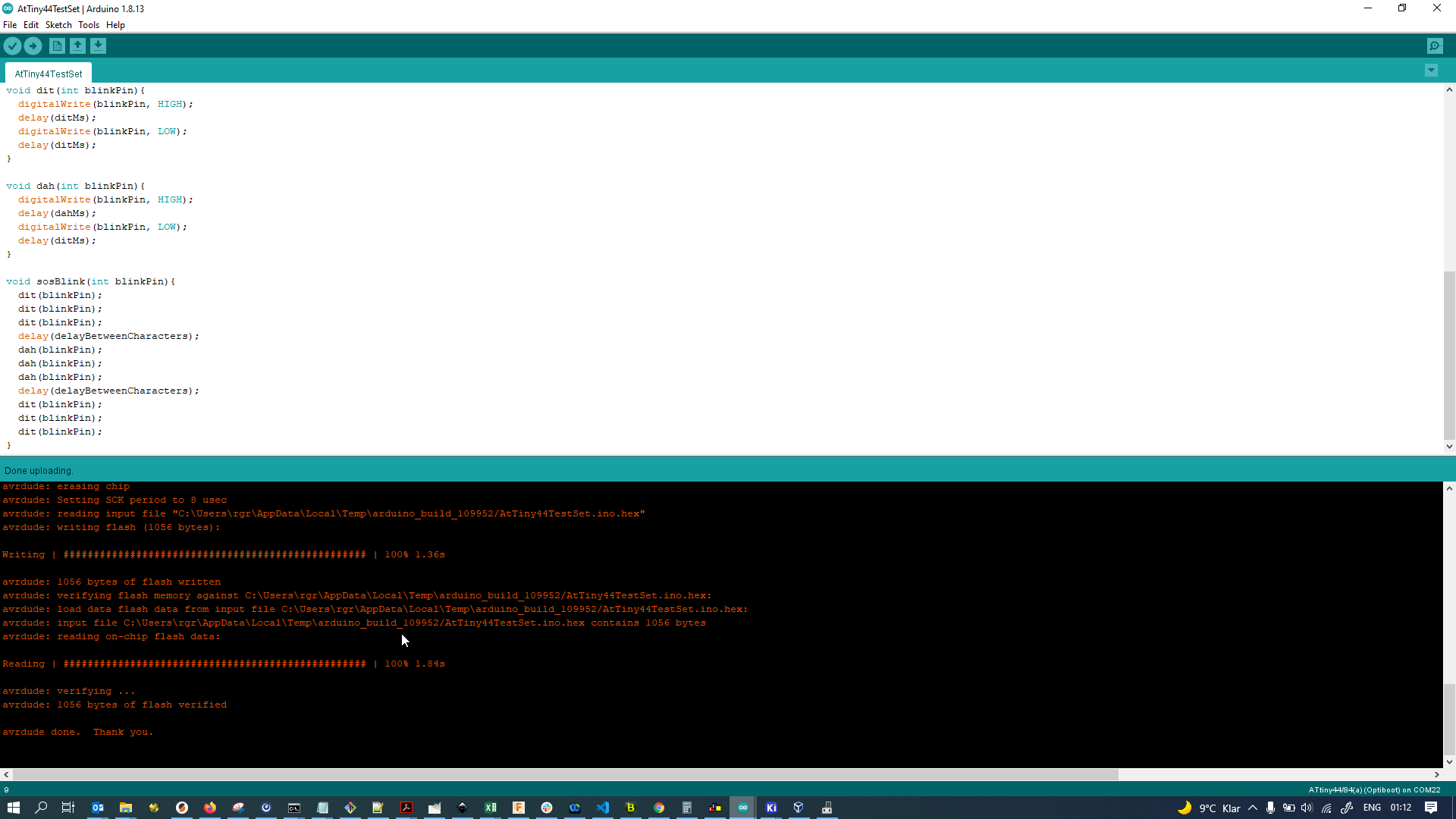
The programmee happily started its little SOS blink sketch:
Later, I did reconnect the solder bridge and programming works fine without an additional power supply. Now I only have to take care not to connect boards for programming that would need a different than 5V power supply or draw more current than the USB port provides. For small boards like this one, it should be perfectly fine though:
-
pcb2gcode unexpectedly crashed. Please report this error to the project manager ↩↩↩
-
pcb2gcode.exe --front _FCU.gbr --back _BCU.gbr --outline _OUT.gbr --drill _DRL.drl --zsafe=5.00 --zchange=10.00 --zwork=-0.50 --metric=true --mill-feed=600.00 --mill-speed=10000 --zcut=-1.8 --cutter-diameter=3.00 --cut-feed=600.00 --cut-speed=10000 --cut-infeed=60.00 --zdrill=-1.80 --drill-feed=1000 --drill-speed=10000↩ -
pcb2gcode.exe --front _FCU.gbr --back _BCU.gbr --outline _OUT.gbr --drill _DRL.drl --zsafe=5.00 --zchange=10.00 --zwork=-0.50 --metric=true --mill-feed=600.00 --mill-speed=10000 --zcut=-1.8 --cutter-diameter=3.00 --cut-feed=600.00 --cut-speed=10000 --cut-infeed=60.00 --zdrill=-1.80 --drill-feed=1000 --drill-speed=10000 --output-dir=outputs↩