6. Electronics design
Week 6 : To do checklist
- Learn and Practice about KiCAD
- Group work
- Learn about the electrical/singal equipents test
- Test and measure the microcontroller circuit board with the equipments test
- Repo to push group work 2022
- Individual Practice
- Design the microcontroller circuit board (schematic/board)
- Mill the microcontroller design
- Programming the microcontroller
- Continue the final Project Process
- Documentations
Assignment (week 6):
Group assignment:
- use the test equipment in your lab to observe the operation of a microcontroller circuit board
Individual assignment:
- redraw an echo hello-world board, add (at least) a button and LED (with current-limiting resistor) check the design rules, make it, and test that it can communicate
- extra credit: simulate its operation
This week I worked on Electronic design
Please click the button for Group Assignment
Group assignment learning
- In the group assignment, we studied the characteristics 3D printer
- What is the best setting of our machine (what it can and cannot do)
- Compared it with another machine
Elektronic Design
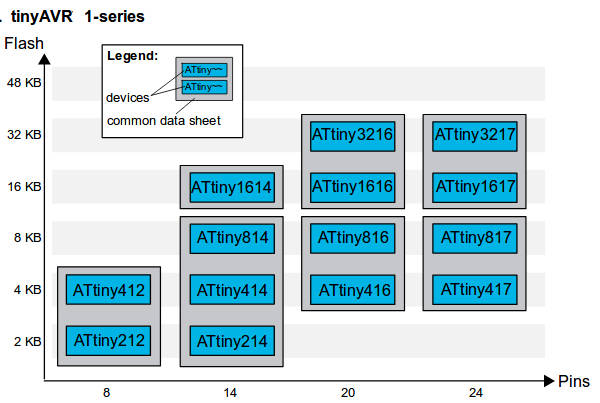
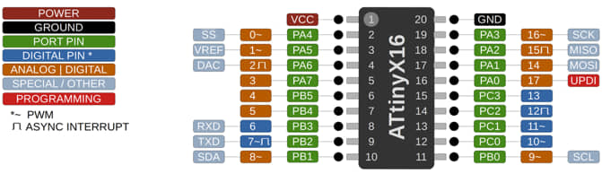
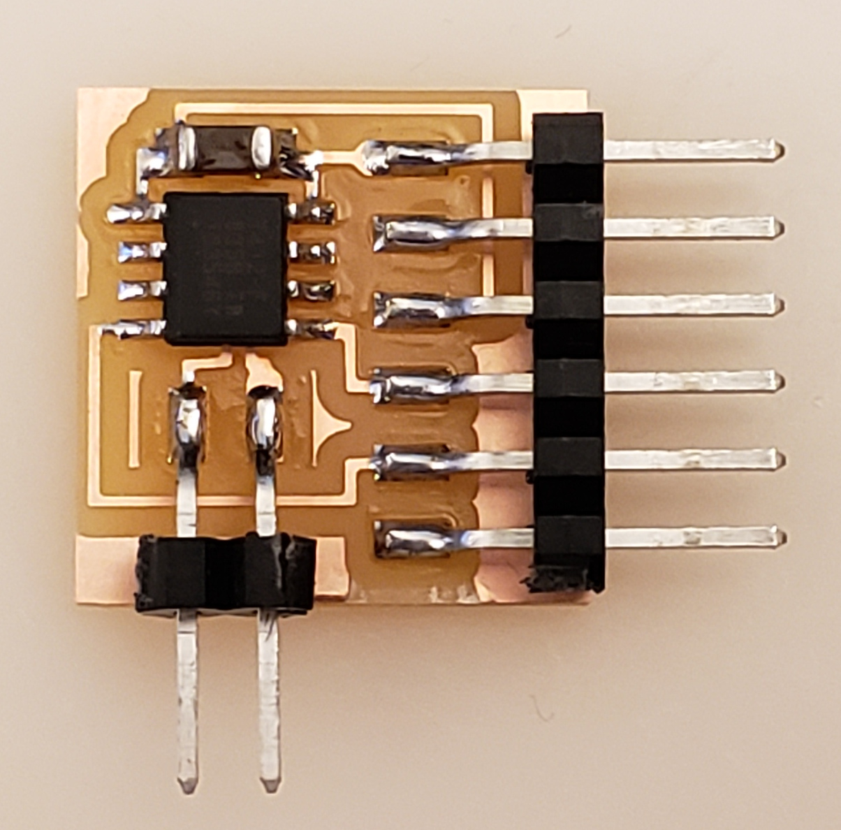
For the microcontroller circuit board I make : - ATTiny 412 - ATTiny 3216
Architecture
Microchip has created the most capable ‘ATtiny’ AVR microcontroller yet, with 32kword of internal flash and a host of analogue peripherals including two 10bit 115ksample/s ADCs (one of which can be used as a touch controller) and three 8bit DACs.
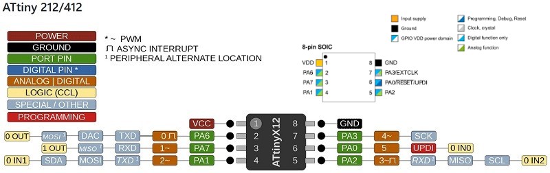
ATTiny 412
The ATtiny412 is a microcontroller using the 8-bit AVR® processor with a hardware multiplier, running at up to 20 MHz and 4 KB Flash, 256B SRAM and 128B of EEPROM in an 8-pin package. The series uses the latest technologies from Microchip with a flexible and low-power architecture, including an Event System and SleepWalking, accurate analog features, and advanced peripherals (source : Microchip).
- Max ADC Resolution (bits) 10
- Number of ADCs 1
- Program Memory Size (KB) 4
- Number of Comparators 1
- CPU Speed (MIPS/DMIPS) 20
- Data EEPROM (bytes) 128
- DigitalTimerQty_16bit 2
- Max 8 Bit Digital Timers 1
- Ethernet None
- I2C 1
- Program Memory Type Flash
- ADC Channels 6
- Low Power No
- Operating Voltage 1.8 - 5.5
- Pin Count 8
- SPI 1
- Temp Range (°C) -40 - 125
- USART 1
ATTiny 3216
The ATtiny3216 series of microcontroller features the 8-bit AVR® processor with hardware multiplier, running at up to 20 MHz and with up to 32 KB Flash, 2 KB SRAM and 256B of EEPROM in 20-pin packages. The series uses the latest Core Independent Peripherals with low-power features. It also includes an Event System, intelligent analog and advanced peripherals. Capacitive touch interfaces with proximity sensing and driven shield are supported by the integrated QTouch® Peripheral Touch Controller (PTC) (source : Microchip).
- Max ADC Resolution (bits) 10
- Number of ADCs 2
- Program Memory Size (KB) 32
- Number of Comparators 3
- CPU Speed (MIPS/DMIPS) 20
- Data EEPROM (bytes) 256
- DigitalTimerQty_16bit 3
- Max 8 Bit Digital Timers 1
- Ethernet None
- I2C 1
- Program Memory Type Flash
- mtrlcntrlinputcapture 2
- ADC Channels 16
- Low Power No
- Operating Voltage 1.8 - 5.5
- outputcomparatorPWM 6
- Pin Count 20
- SPI 1
- Temp Range (°C) -40 - 125
- USART 1
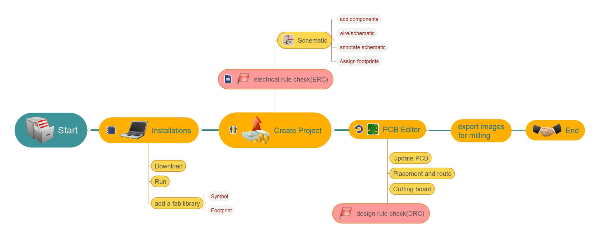
Drawing with KiCAD
KiCad is an open source software suite for Electronic Design Automation (EDA). The programs handle Schematic Capture, and PCB Layout with Gerber output.
KiCad Workflow
Installation
- Download KiCAD
- Install and Run KiCAD
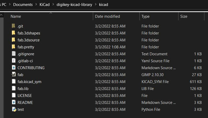
- add a fab library : to add the fab library, we can download the zip or clone the repo
- the source of fab library : fabcloud or repo of CBA.
- sometimes we also need the digikey-kicad-library
- Clone the source of fab library or digikey (position the directory where the library will be cloned)
git clone https://gitlab.fabcloud.org/pub/libraries/electronics/kicad.git
git clone https://github.com/Digi-Key/digikey-kicad-library.git
- after clone or download the library we will get some files
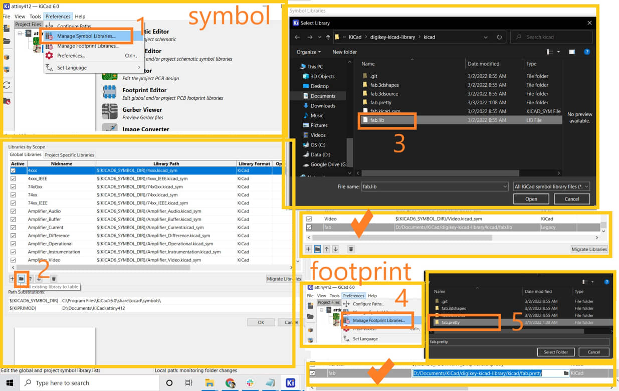
We need to add a library to KiCAD, there are two libraries namely symbols and footprints:
- Run KiCAD
- In Menu Preferences - Manage Symbol Libraries…
- A window appears (Libraries by Scope), select at the bottom “add existing library table”, select the directory to the library folder that we have cloned, select fab.lib. Then the fab library will appear in the Global library.
- Do the same for footprints in Menu Preferences-Manage Footprint Libraries – “add existing library table”, select fab.prety folder. And the footprint library will be included in the Global library
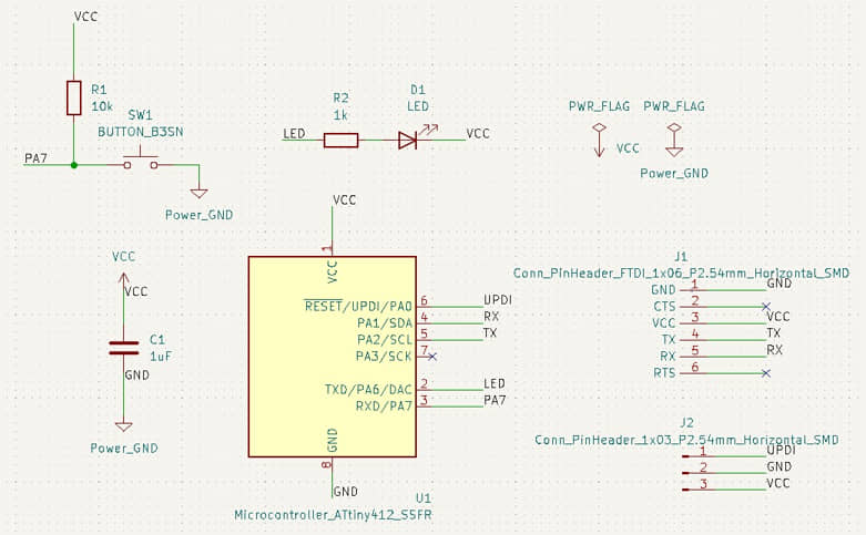
Drawing the ATtiny 412 schematic
I will documented how to handle with KiCad in the context of Electronics Design in Fab Academy. Let us redraw Neil’s hello.t412.echo board with more breakout pins, an LED and a button.
Create the project
The first time we open KiCAD we have to create a project. for example I will create a project “tiny412”
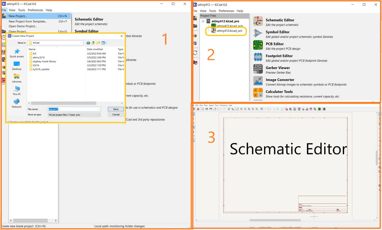
Create the Schematic
In KiCAD one feature that is quite liked is the existence of Hotkeys, we can work quite effectively with these hotkeys. We can check hotkeys by pressing Ctrl+F1 key. Some frequently used hotkeys:
| Hotkey | Description |
|---|---|
| A | Add a new symbol to the sheet |
| R | Rotate |
| M | Move (wires will be disconnected) |
| G | Grab and move a symbol while keeping wires connected |
| L | add a Label |
| W | Start drawing a Wire |
| V | edit Value |
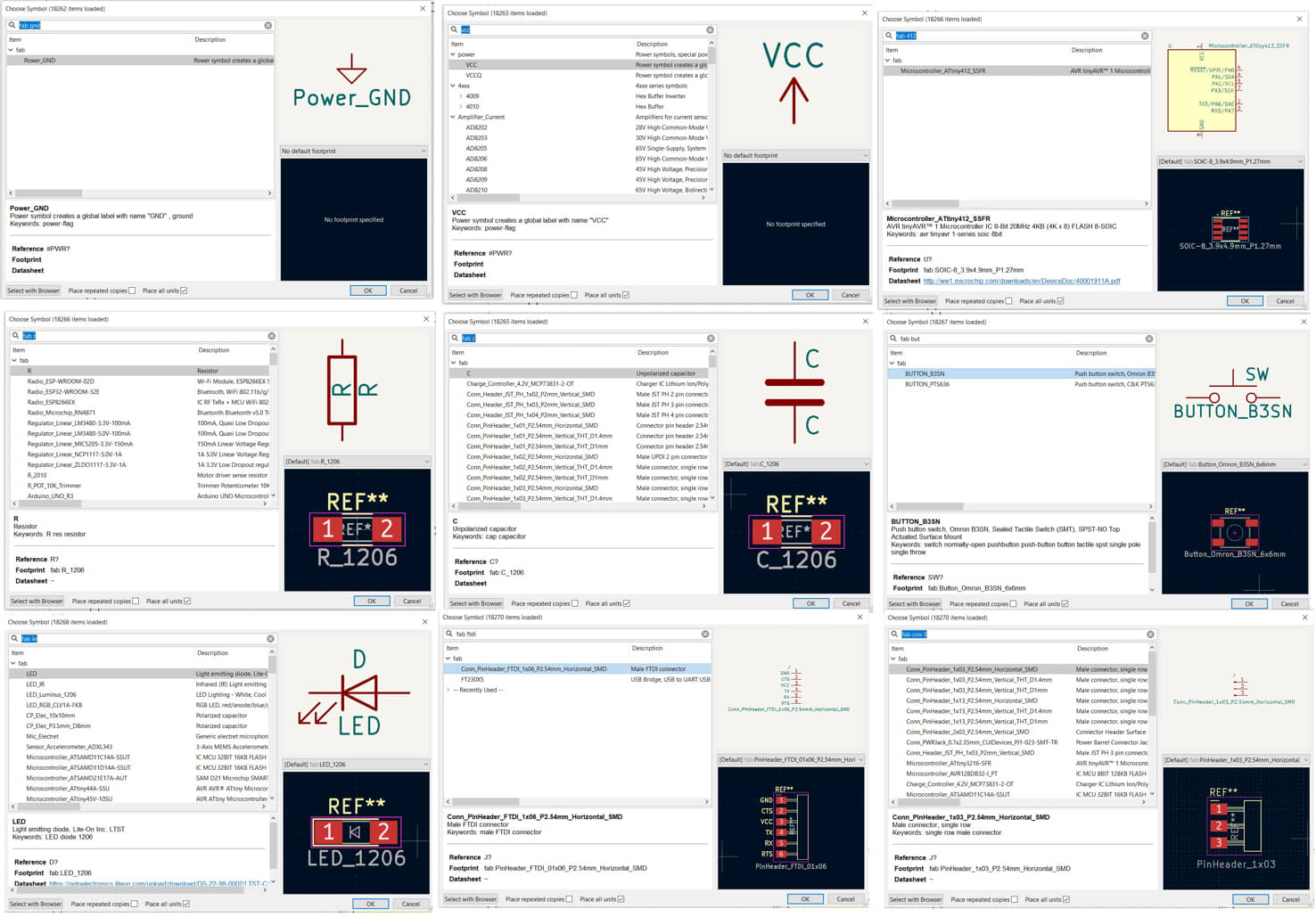
in the schematic editor we will add some components, that is :
 - IC uC      : ATtiny 412
 - Resistors  : 10k, 1k
 - Capacitor  : 1uF
 - Button     : 4 legs
 - LED
 - connectors : 1x6, 1x3 (2.54 mm)
 - others     : VCC, GND, power flags
Add the components by pressing a hotkeys or click toolbar menu add symbol.
- search
fab flagthen OK, place to the schematic editor. Ctrl+D to duplicate the component.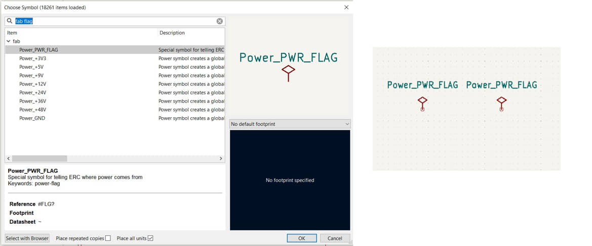
add the other components (search key) and place to the schematic editor (rotate “r”, if needed):
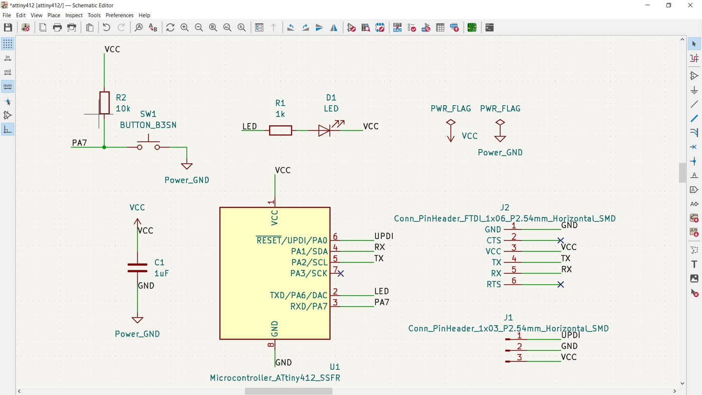
GND (fab gnd); VCC(VCC); resistor (fab r); Capacitor (fab c) ; ATtiny 412 (fab 412); LED (fab led); connectors 1x6 (fab ftdi); connectors 1x3 (fab con 3).
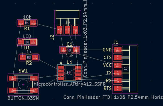
and the schematic editor :
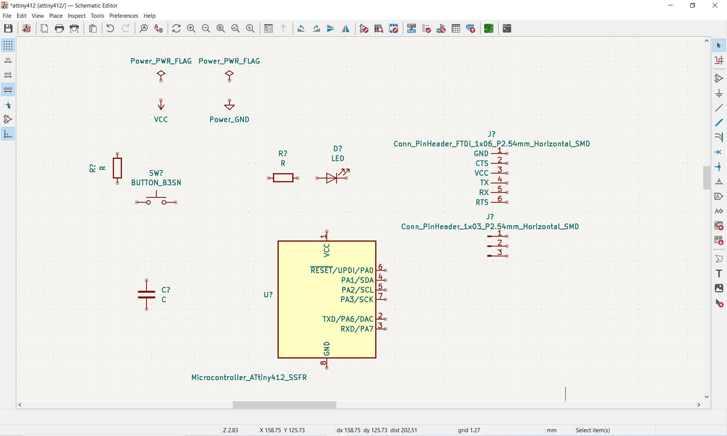
Positioning the component and make the wire connect between components or make the Label wires
- connect the power flag with VCC, and also the another power flag with GND
- connect the resistor to the LED, do for other component
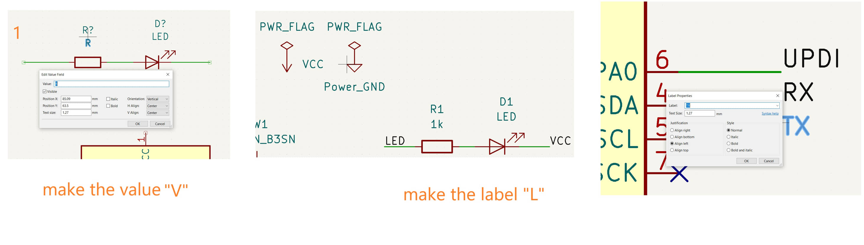
- add the value “V” of the component (resistor with 1k, 10k, capacitor with 1uF)
- if the number of connections is large, it would be better to use a label wire. We just need to label a connector, so if there is another connector with the same name, it will be automatically connected with the same label without having to make wires directly between components.
- i will name each pin on attiny 412 with a label. Previously I needed to create an extension wire for the label point. Press “L”, then give the name label, place to the point connector.
Warning
labeling must be consistent and the same name for the same junction, pay attention to uppercase and lowercase letters
The final circuit becomes like this
Annotate schematic
Usually at the beginning of schematic creation, component annotations are not formed directly (automatically) so we need to Annotate schematic so that the component numbering sequence can be good. We do this with the menu: Tools - Annotate schematic - Annotate. Then all components will be annotated.
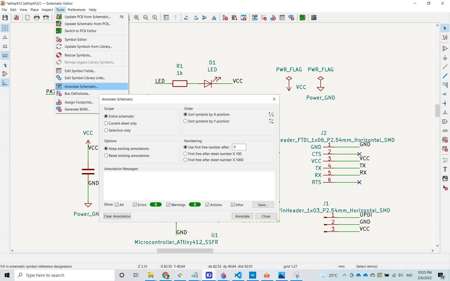
Components are now annotated.
Electrical rule check(ERC)
Electrical rule checking (ERC) is a methodology used to check the robustness of a design both at schematic and layout levels against various “electronic design rules”. These design rules are often project-specific and developed based on knowledge from previous tapeouts or in anticipation of potential new failures.
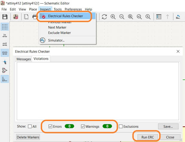
If the circuit is correct then no error will appear
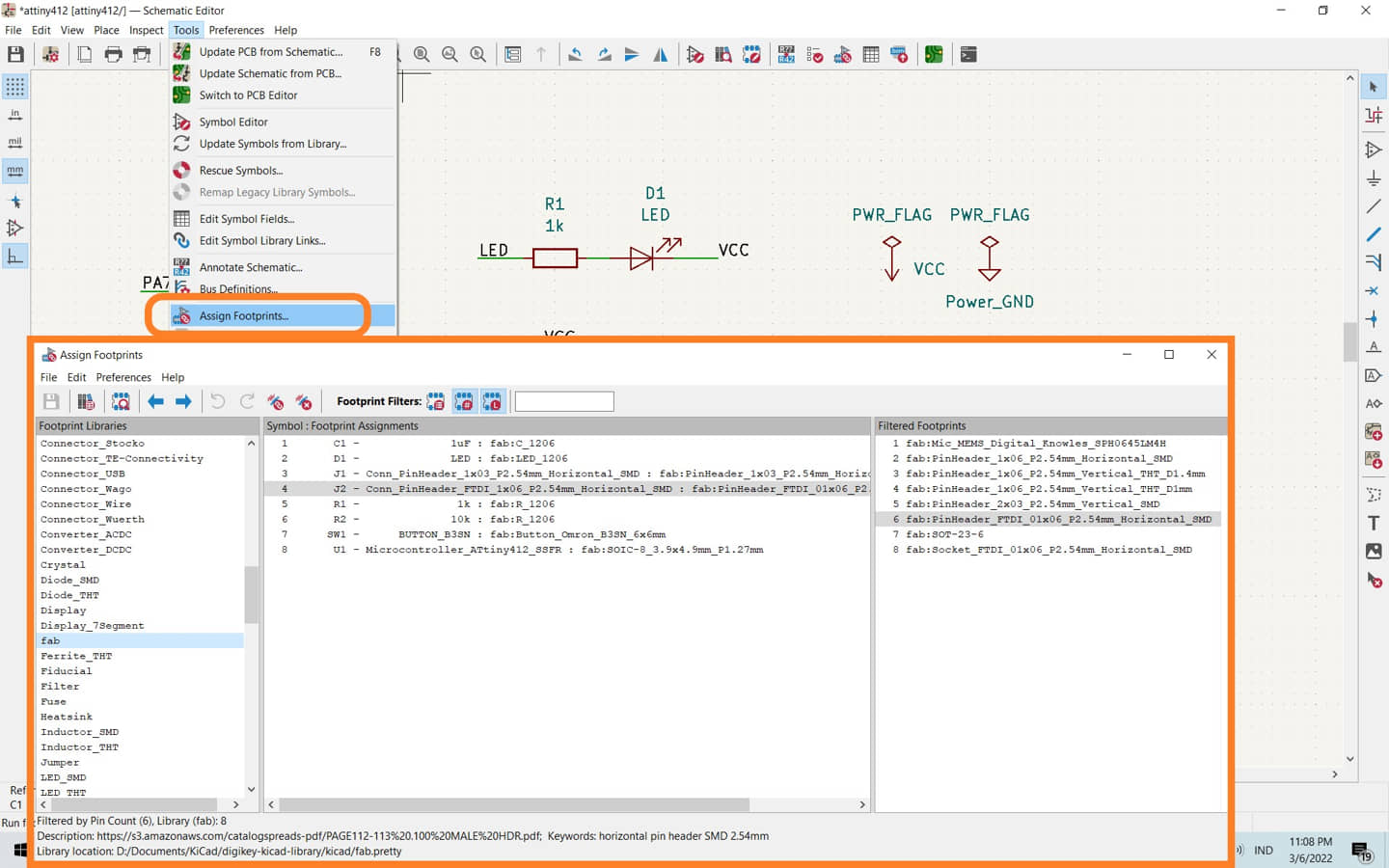
Footprint Assignment
Before entering into the PCB board design, we must make sure the shape of the feet that will be printed on the board is the same as the components that we will install later. Therefore we need to re-check the shape of the footprint. Footprints will usually be installed automatically if we have previously added the footprint library. But there are times when the footprint cannot be loaded, so we need to load it manually.
In the middle of the window display is the component that we use. Check whether each component already has the appropriate footprint shape. If not we can start selecting our components (middle box) and choose from the left box (source template footprint library), then we select the appropriate footprint shape in the right box. We can also see the footprint shape image from the footprint viewer menu.
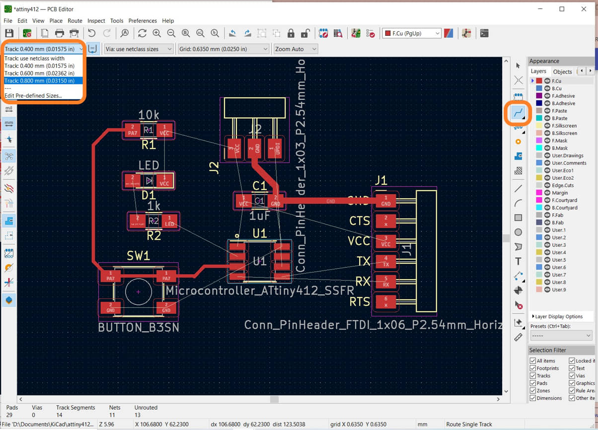
PCB Editor
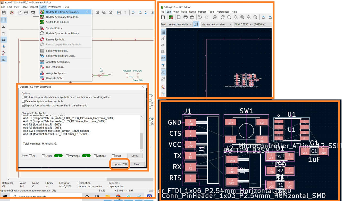
After all the steps in the schematic editor are complete and OK, we can start working on the PCB board.
- Update PCB, put components in PCB editor
- adjust the position of components to make it easier to create paths. if necessary rotate “R”, and shift components. It would be better if the space board used was getting smaller.
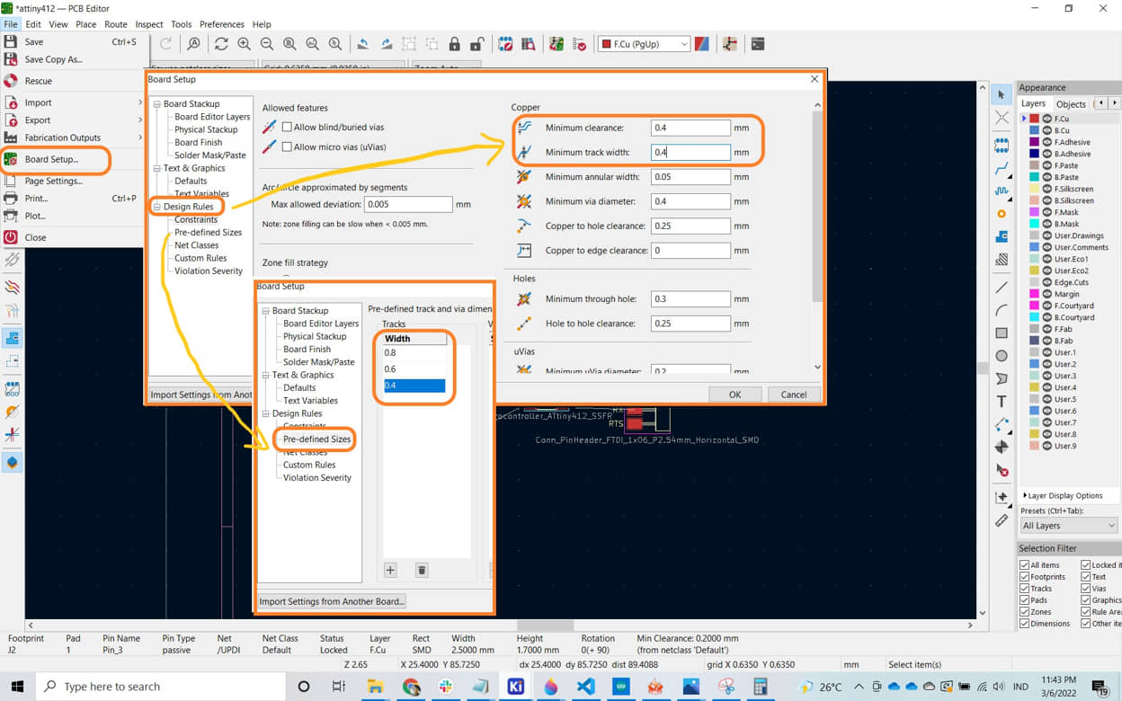
Design rules
When the PCB will be milled, we will use the smallest milling chisel, which is 1/64” (0.4 mm), so we need to set a clearance that can be made, which is 0.4 mm.
Components are positioned, as an early stage to create a route, there may be changes when creating a route, to get the best component position.
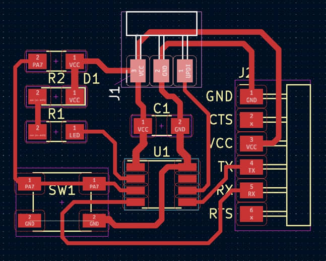
Create a route track based on the wire connection that has been made. The size of the track can be adjusted according to the board configuration that we entered earlier. Usually for power lines (VCC, and GND) we make the lines larger (0.8 mm) while for data we can make them 0.4 mm or 0.6 mm.
and the PCB track results become:
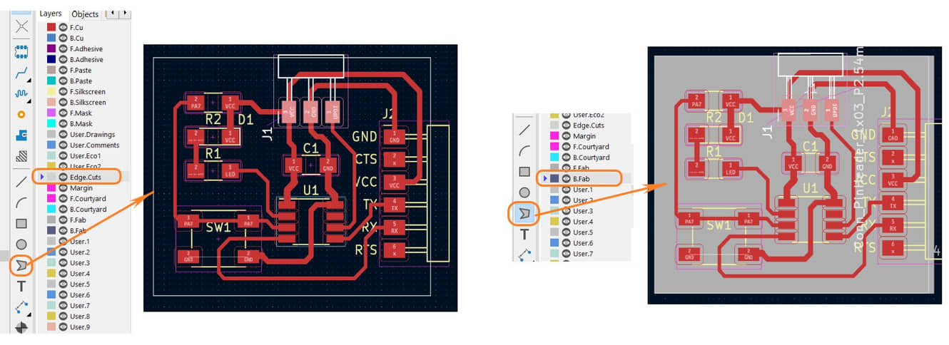
Make the interior/cutting board
The circuit route path has been created, we just need to make a cut path shape for the board. It is used for the path to be milled for the outer shape (interior) of the PCB board. For that we need to change the layer to “Edge Cut”, then draw the outer board. Do the same for B.Fab layer, and make the area of the board.
Design Rule Check(DRC)
Design Rule Checking (DRC) verifies as to whether a specific design meets the constraints imposed by the process technology to be used for its manufacturing. DRC checking is an essential part of the physical design flow and ensures the design meets manufacturing requirements and will not result in a chip failure.
To ensure that the PCB path to be made has no errors, we do DRC. From the Inspect menu - Design Rules Checker
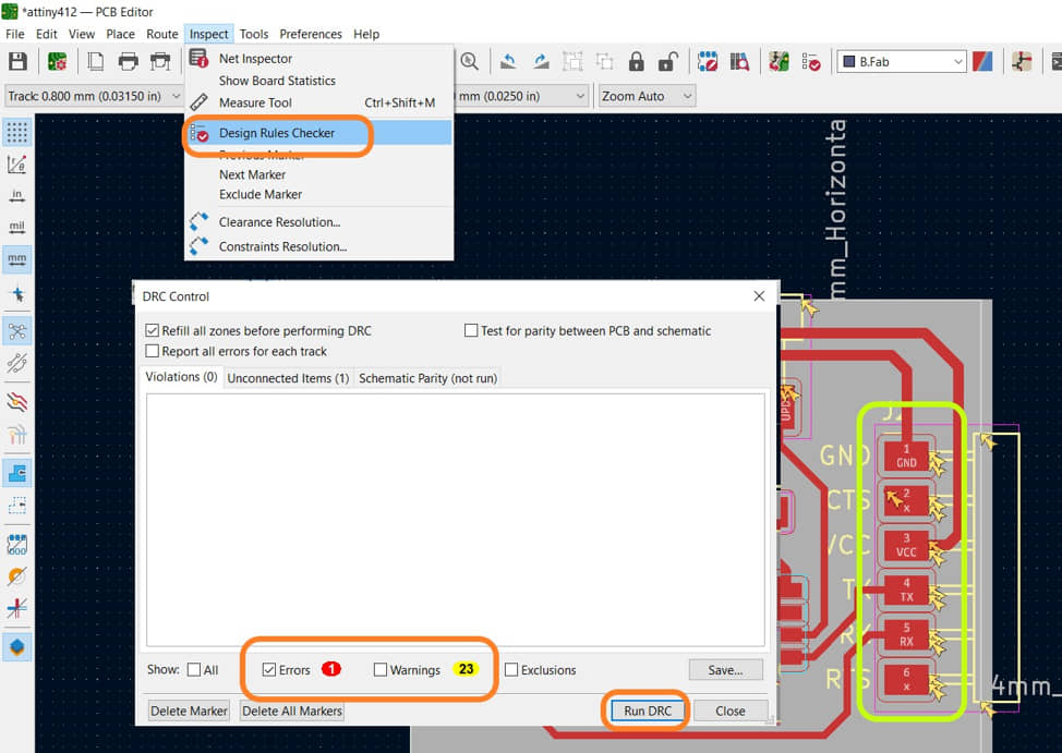
We find that there are no errors in this circuit. however there are several warnings issued. Warnings don’t cause circuit errors (so they can be ignored), but will recommend better pcb results. For PCB design, we ignore this warning.
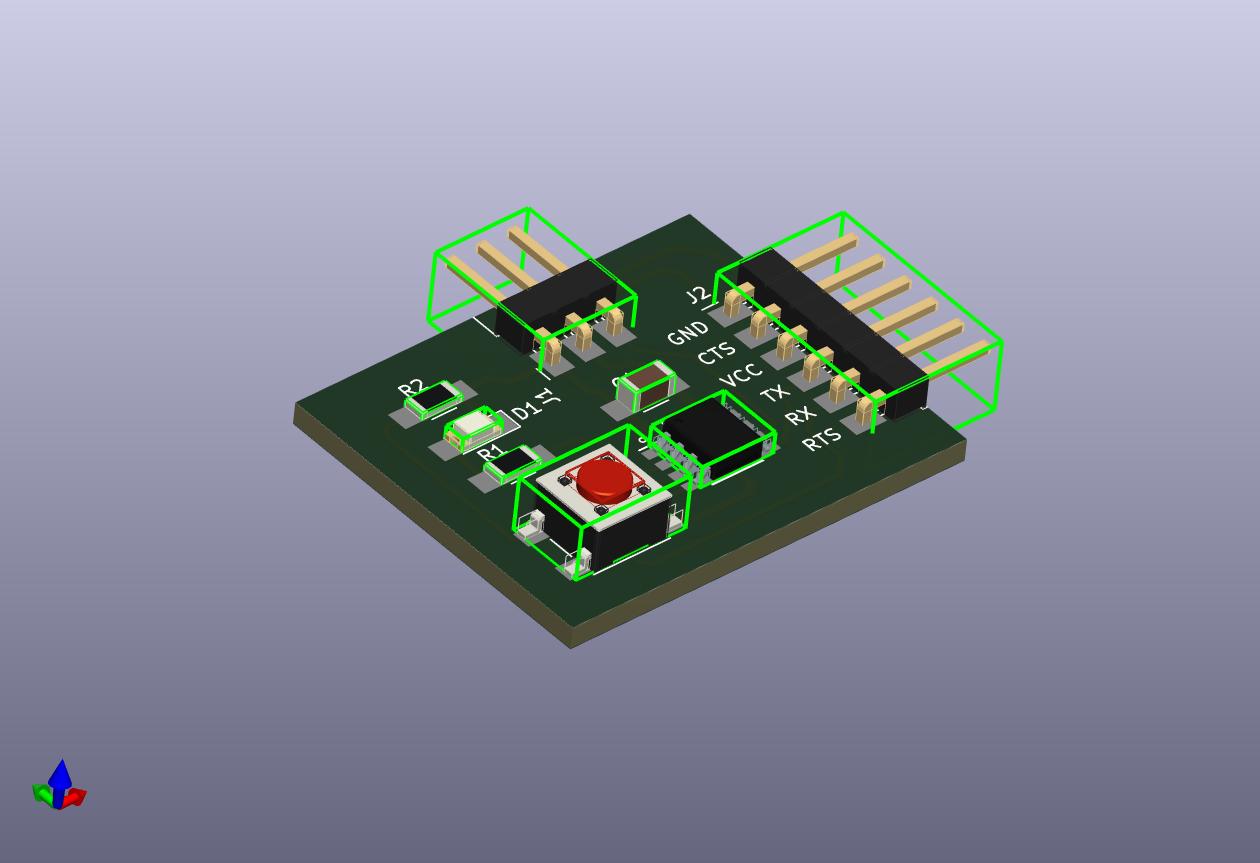
We can see the 3D view by clicking : view -3D Viewer
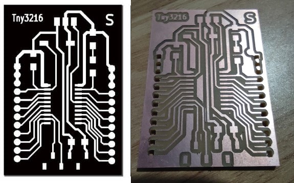
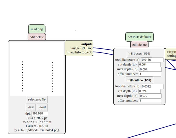
export images for milling
To prepare the design for milling, we will export the trace image and the interior of the board. The step is with the menu export - SVG; check the F.Cu cooper layer and export for the trace path, and change the check to B.Fab for technical layer to make the interior path.
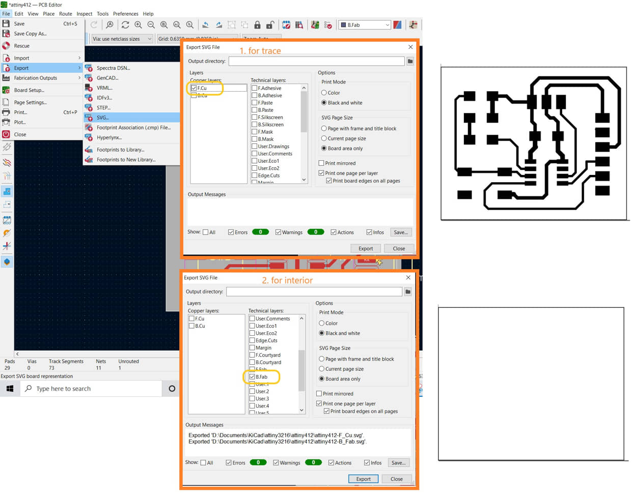
and we get the SVG files for source of MODS mill
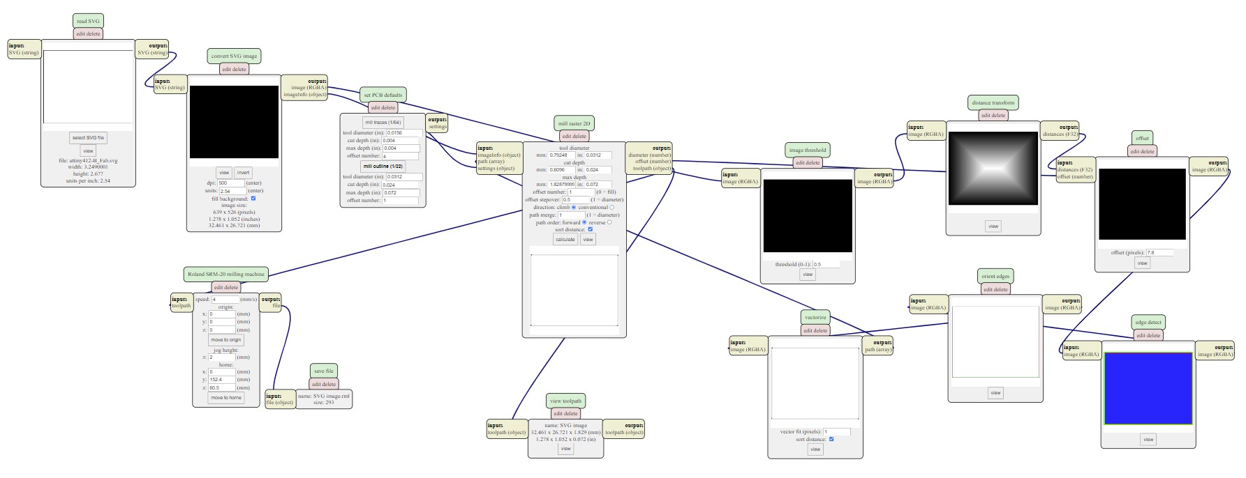
Mill the boards
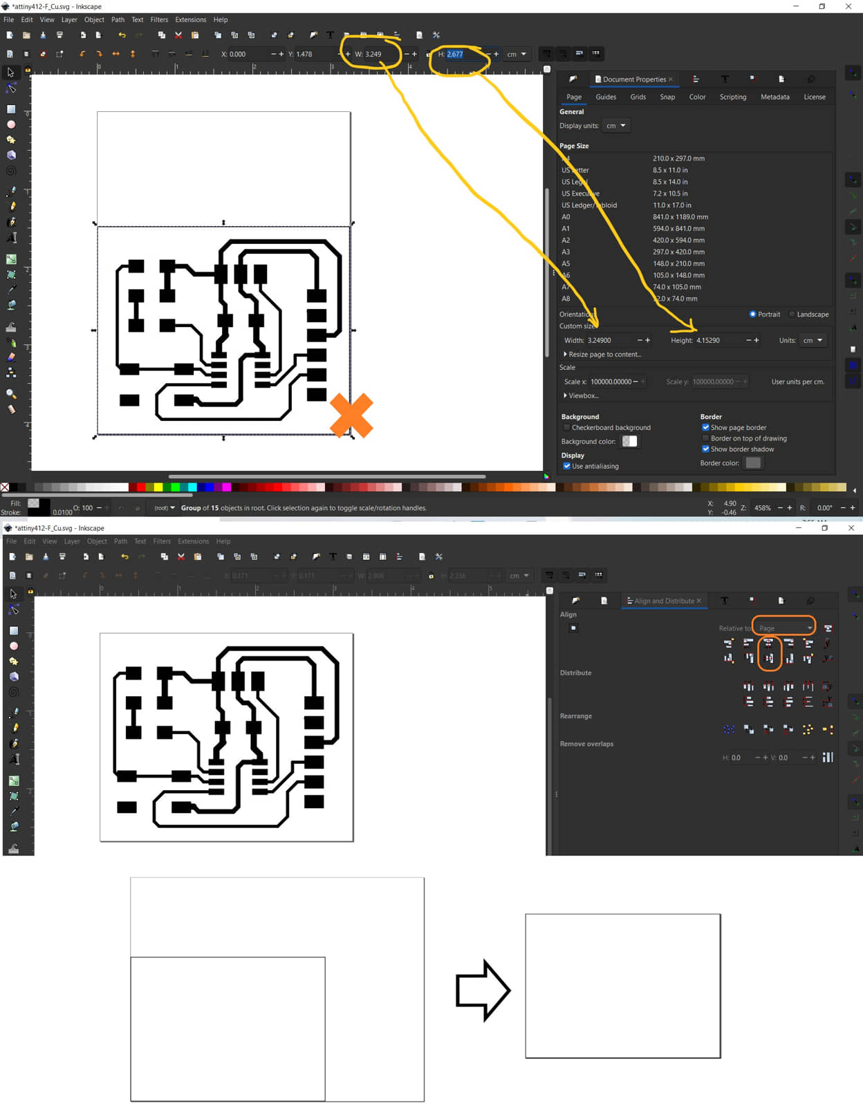
When going to use the source of the SVG export, we need to slightly edit the SVG file, namely adjusting the document size to the size of the board that we created.
- Open the route board file (attiny412-F_Cu.svg), click on the outer object of the PCB track, the length and width will appear. Enter this value in the Document properties.
- Remove outline line (optional)
- set align object trace with page in horizontal and vertical center position.
- do the same for the interior board file (attiny412-B_Fab.svg)
- Open the MODS here
- Select the program - open server program - Roland SRM 20 svg; add the modul for file save
- Open the .svg files (attiny412-F_Cu.svg)
- Invert the image
- Set origin to x0, y0, and z0
- Select the mill trace (1/64)
- Calculate the mods, and we will get the view of cnc toolpath and automatically download the rml files.
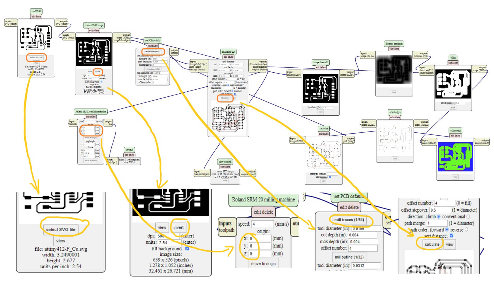
- Do the some process with the interior svg file (attiny412-B_Fab.svg), change to Mill outline 1/32
 - Go to the machine,
- install tool diameter (1/64 for trace, 1/32 for interior)
- Open the VPanel SRM-20 software, setting datum origin.
- Running the rml files (trace and interior)
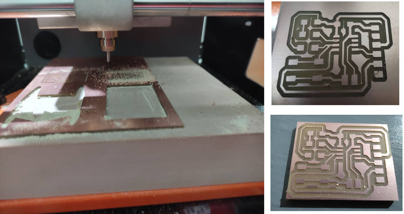
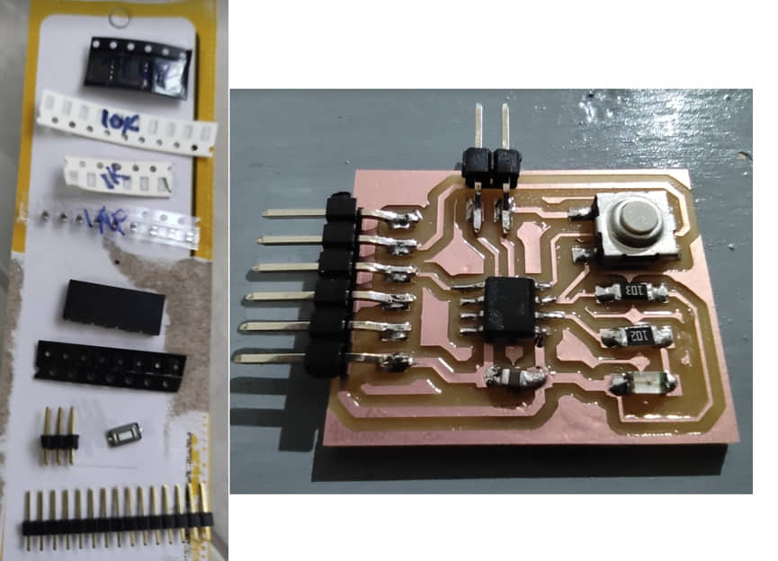
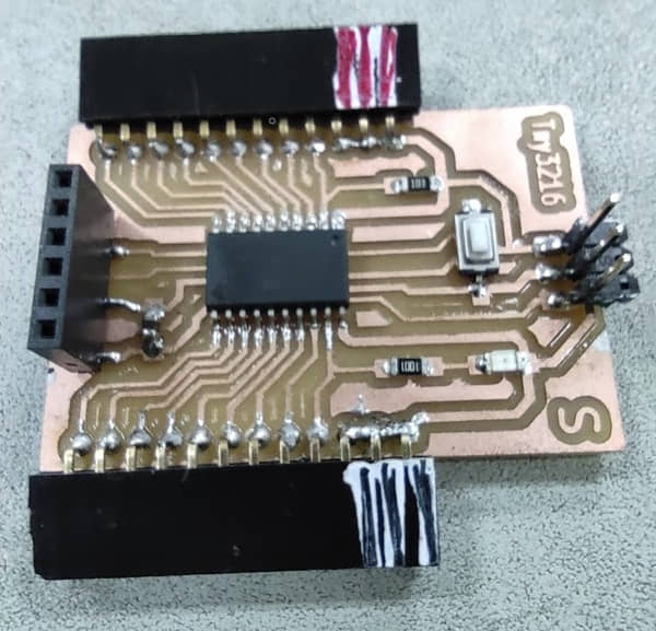
Soldering
After the PCB is finished, we prepare:
- Components and soldering station
- Solder the components according to their position, don’t forget to give flux
- check and test the circuit
Programming
In this microcontroller we will try three programs: (blink led, blink led with button, echo).
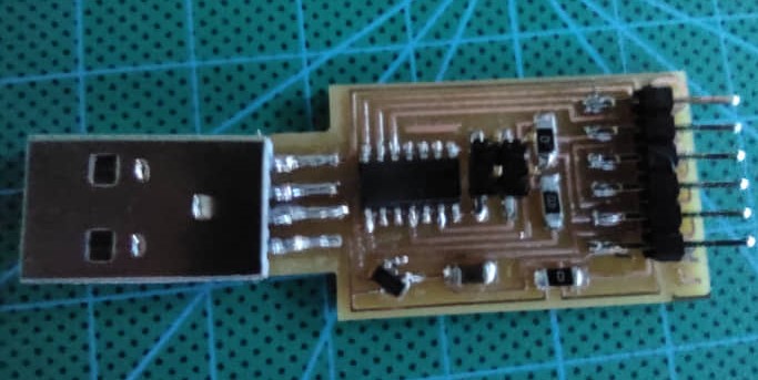
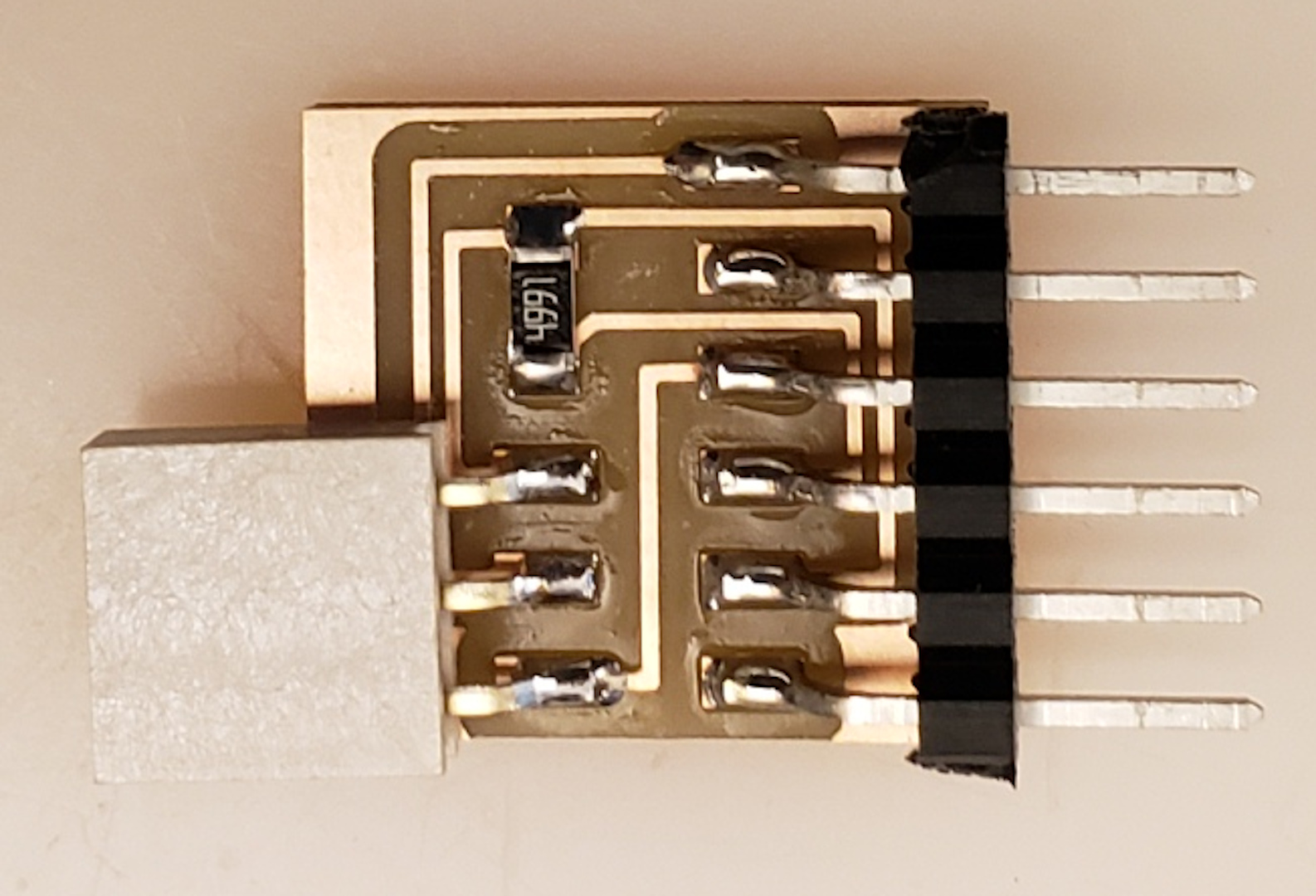
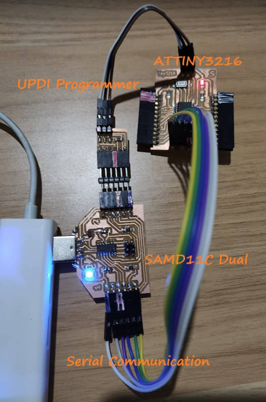
To program (upload sketch) on this ATTiny 412 bord we need a USB SAMD11C Serial, and an UPDI board.
We can use SAMD11C USB to uploading the sketch (with UPDI board), and we can use theto communicate with ATtiny412 via pin 6 wire.
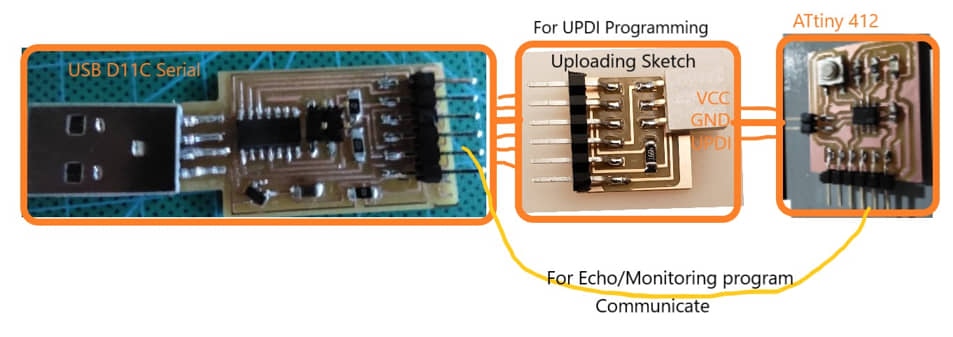
- plug SAMD11 on USB, check in device manager where COM is installed, install Attiny 412 (with UPDI board) as shown above.
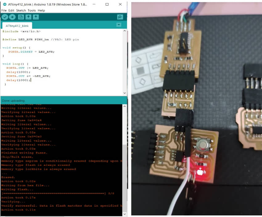
Code for Blink
- Open the blink412.ino program with Arduino IDE
#include <avr/io.h>

#define LED_AVR PIN6_bm //PA3: LED pin

void setup() {
   PORTA.DIRSET = LED_AVR;
}

void loop() {
  PORTA.OUT |= LED_AVR;
  delay(1000);
  PORTA.OUT &= ~LED_AVR;
  delay(1000);
 }
- Configure the tools in the IDE as shown below
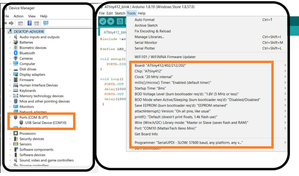
- upload the sketch to attiny 412
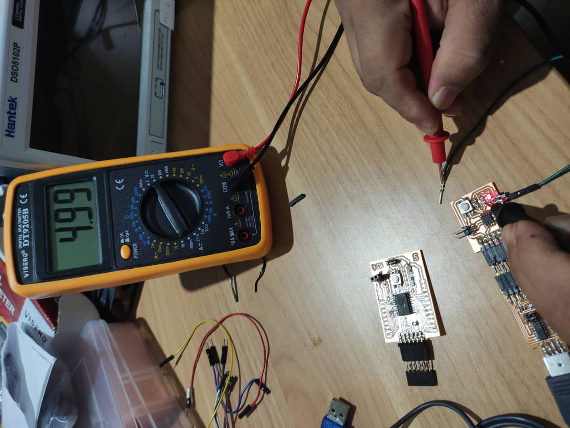
Check the connection with digital Multimeter
I tried to measure the connection and voltage on the MCU 412. The measured VCC voltage was 5.02 V. then I measured the voltage at pin 2, when the LED is on the measured voltage is 4.99V and when it’s off the voltage is 0V.
Code for Blink with Button
In this program added a button to turn on the led
- Open the ATtiny412_blink_button.ino program with Arduino IDE
#include <avr/io.h>

#define LED_AVR PIN6_bm //PA6: LED pin
#define BUTTON_AVR PIN7_bm //PA7: Button pin

void setup() {

   PORTA.DIRSET = LED_AVR;    // use LED pin as an output
   PORTA.DIRCLR = BUTTON_AVR; // use Button pin as an output
}

void loop() {
/** HIGH/LOW Instruction
  PORTA.OUT |= PIN4_bm; // write PA4 high
  PORTA.OUT &= ~PIN4_bm; // write PA4 low
**/
  bool state = PORTA.IN & BUTTON_AVR; // read the state of a pin
  switch(state) {
    case 0:
    PORTA.OUT &= ~LED_AVR;
    break;
    case 1:
    PORTA.OUT |= LED_AVR;
    break;
    default:
    PORTA.OUT &= ~LED_AVR;
    break;
  }
 }
- upload the sketch to attiny 412
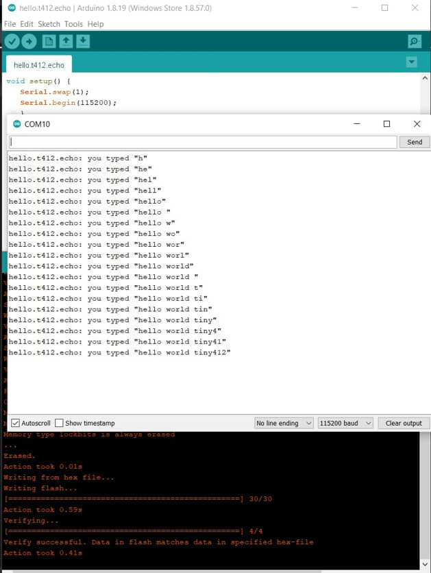
Code for echo
In the program we will use tiny412 for communication via serial.
- Open the hello.t412.echo.ino program with Arduino IDE
//
// hello.t412.echo.ino
//
// tiny412 echo hello-world
//    115200 baud
//
// Neil Gershenfeld 12/8/19
//
// This work may be reproduced, modified, distributed,
// performed, and displayed for any purpose, but must
// acknowledge this project. Copyright is retained and
// must be preserved. The work is provided as is; no
// warranty is provided, and users accept all liability.
//

#define max_buffer 25

static int index = 0;
static char chr;
static char buffer[max_buffer] = {0};

void setup() {
   Serial.swap(1);
   Serial.begin(115200);
   }

void loop() {
   if (Serial.available() > 0) {
      chr = Serial.read();
      Serial.print("hello.t412.echo: you typed \"");
      buffer[index++] = chr;
      if (index == (max_buffer-1))
         index = 0;
      Serial.print(buffer);
      Serial.println("\"");
      }
   }
- upload the sketch to attiny 412 via UPDI, after upload change the connection SAMD11C to ATtiny via 6 wire
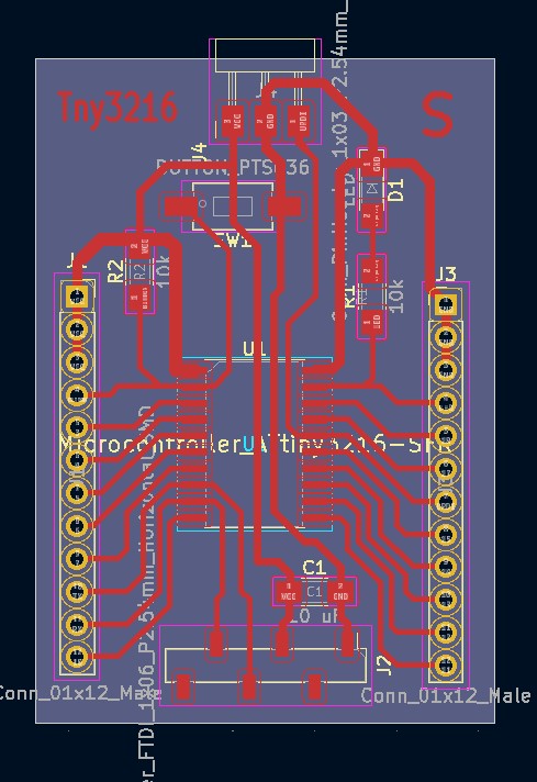
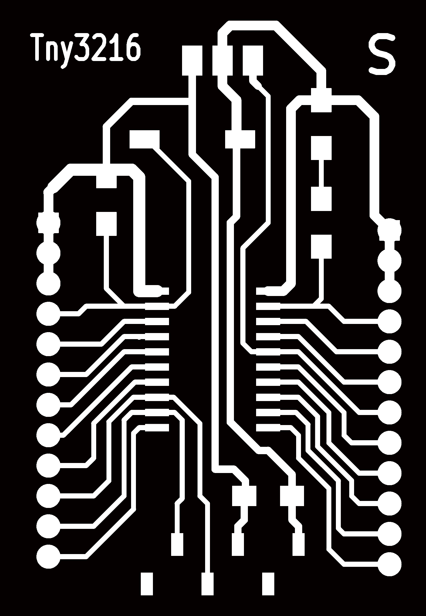
Another board (ATtiny 3216)
This MCU have 20 pin (more than ATtiny 412 pin)
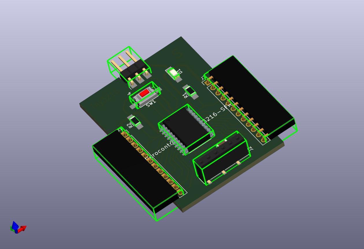
Desain the schematic and PCB board
3D Viewer
Production of PCB board (mill and soldering)
make through holes
To make a through holes on PCB, there are several steps to take:
- The footprint setting has been made using the through hole type.
- after the trace (F.Cu) is exported in svg, make edits to trace PCB using inkscape, save as the svg file to other svg file (the for hole mods process)
- for Trace process (Origin F.Cu file):
- fill the hole with black for trace
- Execute Mods procedure for trace mill using SVG source
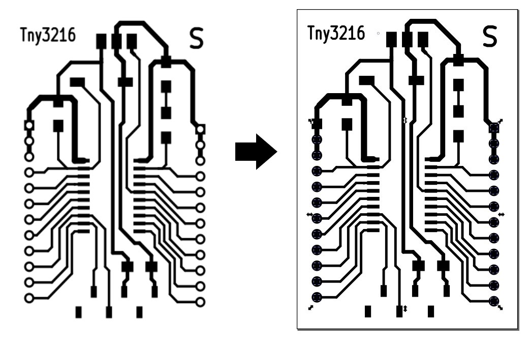
- for Holes : (Copied F.Cu file) :
- Delete the trace part, leave the hole, fill the hole with black for outline.
- Execute Mods procedure for *mill outline using SVG source
- Use tool size 1/64
Programming
Using the SAMD11 Dual Serial (continue from week-4)
Continuing from Week 4 (about making SAMD11 dual serial) here I try to use it to use it in the echo.serial program on the attiny-3216 board. Using the dual serial SAMD11C there is no need to remove and attach cables or use two SAMD11s.
References
- Kamakura : KiCad tutorial
- KiCAD - Fab Library Installation (Windows)
- KiCAD 6.0 Tutorial
- Electronics Design
- Embedded Programming
- Codes for AVR Boards
Documentation Files
- blink for tiny 412
- blink button for tiny 412
- hello echo for tiny412
- blink for tiny 3216
- blink button for tiny 3216
- hello echo for tiny3216
- ATtiny412 route (svg)
- ATtiny412 interior (svg)
- ATtiny3216 route (png)
- ATtiny3216 route (svg)
- ATtiny3216 interior (png)
- ATtiny3216 holes (png)
- ATtiny 412 Schematic KiCAD
- ATtiny 412 Board KiCAD
- ATtiny 412 Project KiCAD(zip)
- ATtiny 3216 Schematic KiCAD
- ATtiny 3216 Board KiCAD
- ATtiny 3216 Project KiCAD (zip)
- Samd 11 Dual Schematic KiCAD
- Samd 11 Dual Board KiCAD
- Samd 11 Dual Project KiCAD (zip)
Lessons learned (week 6 : Electronics design):
- Understand how electronics components and MCU work
- Understanding and Applying Design Circuit with KiCAD
- Applying the design circuit, make the PCB, soldering and programming
- understanding how the test tools electronics work
- Understanding how the MCU can used in my final project