4. Electronics production
Week 4 : To do checklist
- Learn about 2D CNC Operations
- Group work
- CNC Mini router charachteristic
- Repo to push group work 2022
- Individual Practice
- Design circuit (include the microcontroller)
- Mill and stuff the PCB
- Programming and test the PCB
- Continue the final Project Process
- Documentations
Assignment (week 4):
Group assignment:
- characterize the design rules for your in-house PCB production process extra credit: send a PCB out to a board house
Individual assignment:
- make an in-circuit programmer that includes a microcontroller:
- extra credit: customize the design
- mill and stuff the PCB
- test it to verify that it works
- extra credit: try other PCB processes
This week I worked on Electronics production
Please click the button for Group Assignment
Group assignment learning
In the group assignment, we studied the characteristics of the design rules for in-house PCB production process :
Circuit Programmer Design
In this task I will create :
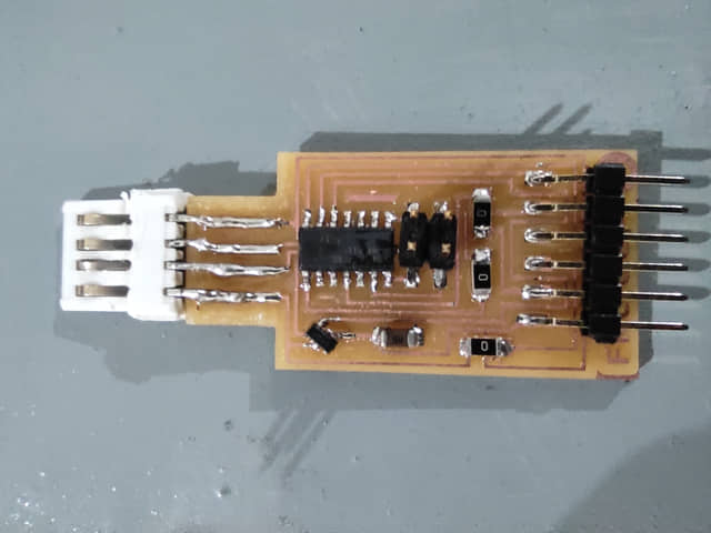
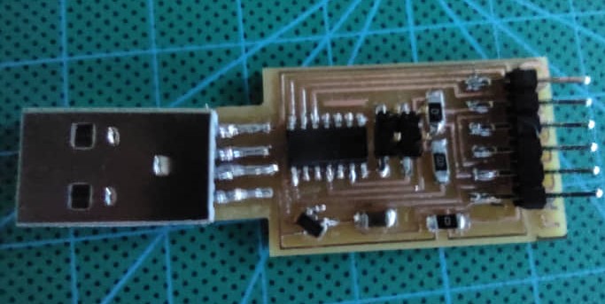
- Circuit programmer “SAMD11C USB-serial”
- ATTinny 412 board
- Customize PCB for Programming and ATTINY
Design the PCB board
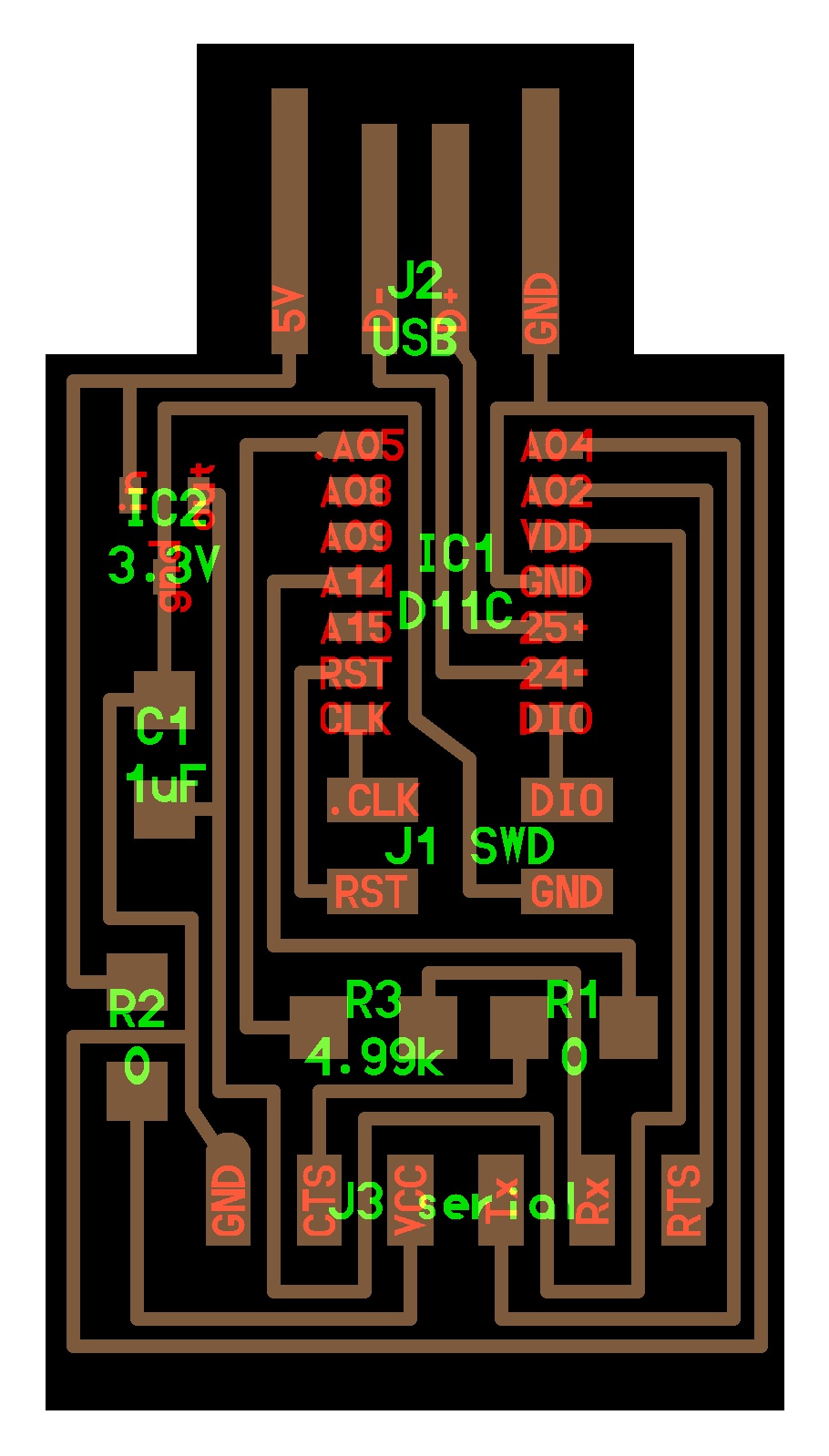
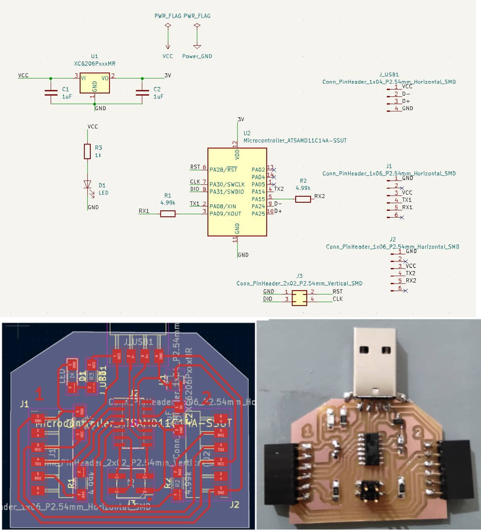
USB-serial SAMD11C circuit for the board**
Information (github.com/wagiminator)
The SAMD11C14A is a low-power microcontroller using the 32-bit ARM Cortex-M0+ processor with 16KB Flash and 4KB of SRAM. The SAM D11C14A operates at a maximum frequency of 48MHz and reaches 2.46 Coremark/MHz. It includes intelligent and flexible peripherals, Event System for inter-peripheral signaling, and support for capacitive touch button, slider and wheel user interfaces. The SAM D11C14A is compatible to the other product series in the SAM D family, enabling easy migration to larger device with added features.
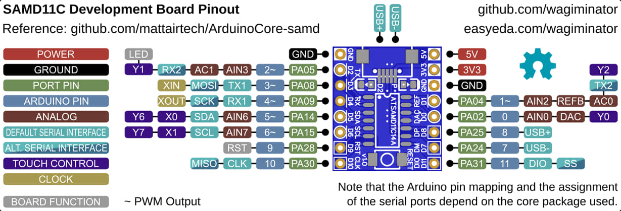
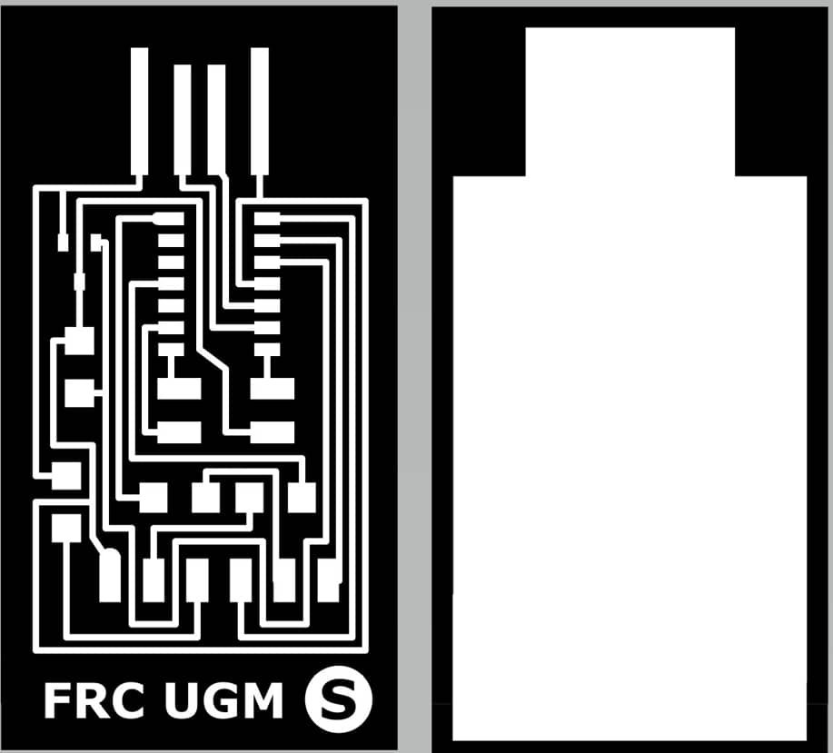
Incidentally for this task, the USB-serial SAMD11C board design has been provided on Fab Academy lecture (components, board, route, interior ) and I just need to download it (the route and interior files (.png)).
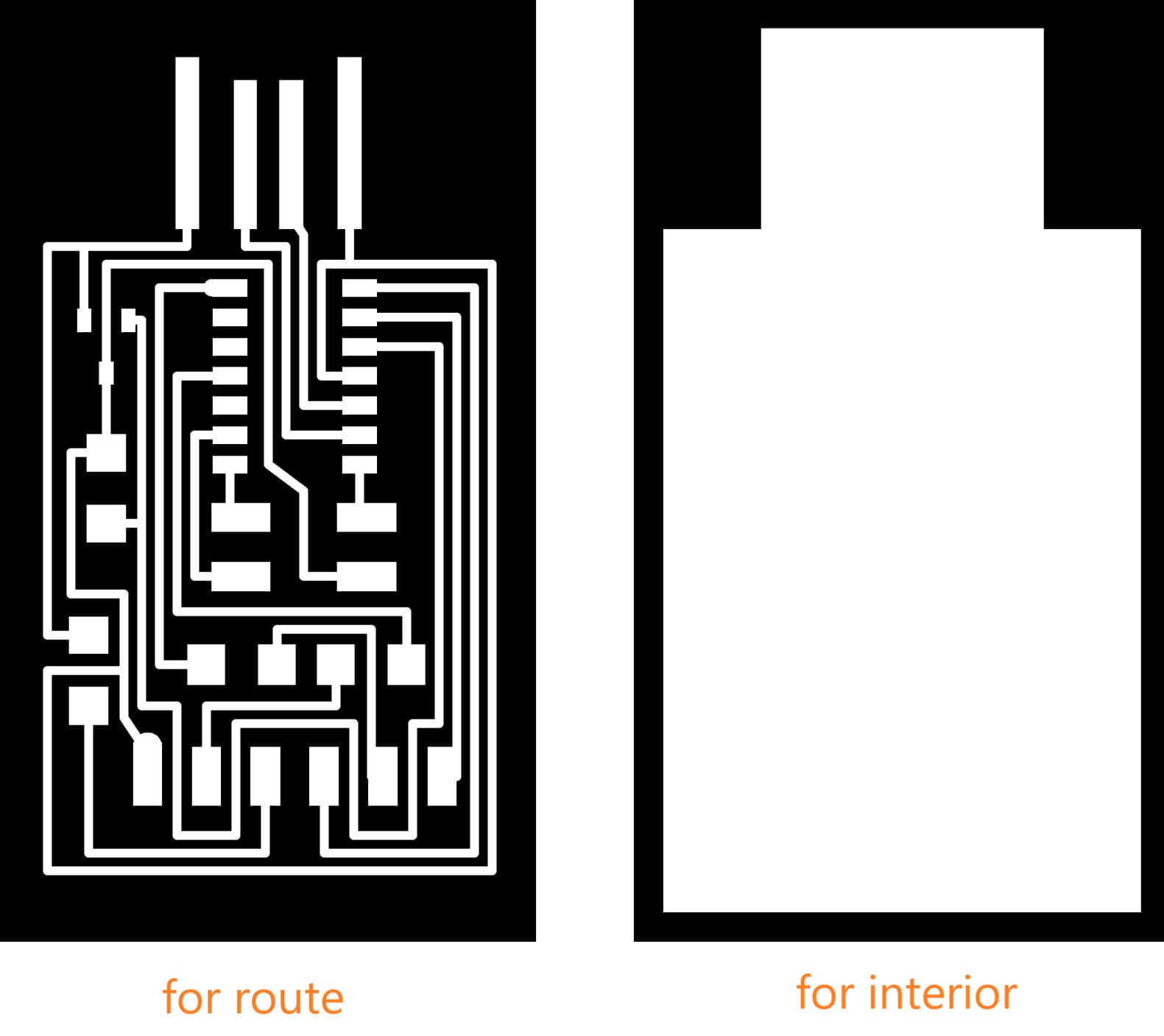
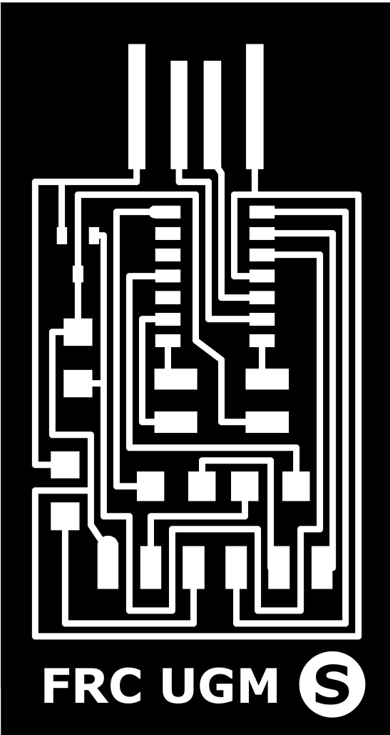
I also tried to change the SAMD11C file that I downloaded and added the initials using Inkscape. then I export the results to png with a dpi of more than 600dpi. Likewise for the interior, I adjusted the dimensions according to the route board.
ATTINY 412 board
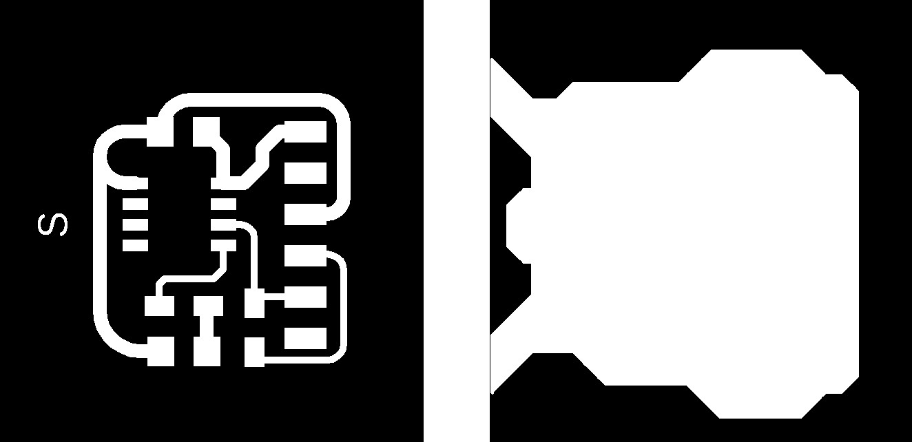
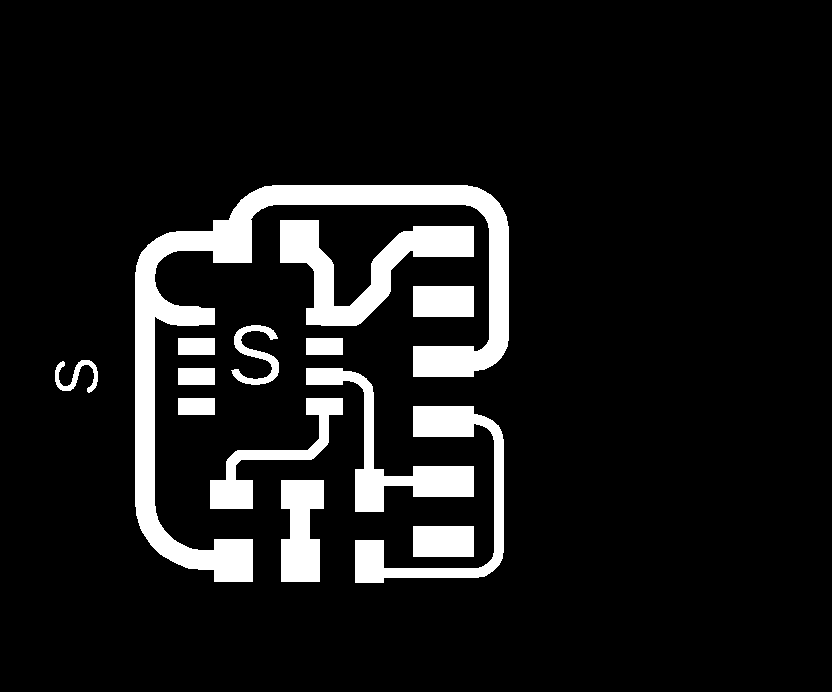
For the minimum system design on the microcontroller. I’m using ATTINY 412. The design of the board is made of twists and turns to form a cat’s head image.
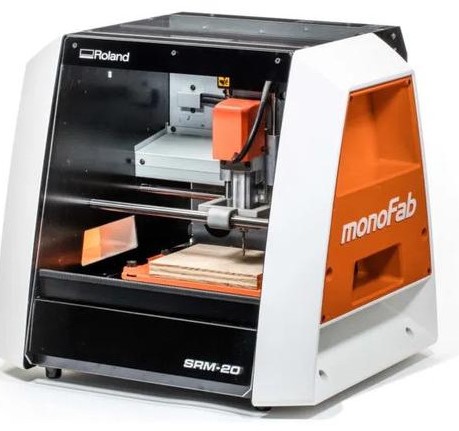
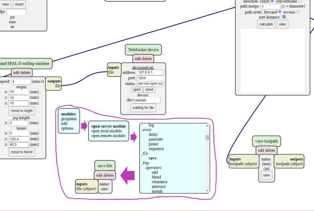
Make G Code using MODS for cutting on the CNC mini Router
The CNC Mini router used is Roland SRM-20
- Uses MODS (can be found here)
Info
MODS is an online tool developed by Niel’s Center for Bits and Atoms used to convert image files to milling files.
- MOD for Trace ( Right Click - program-open server program- chose the CNC Mini Router type (Roland SRM20)
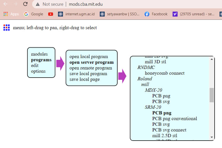
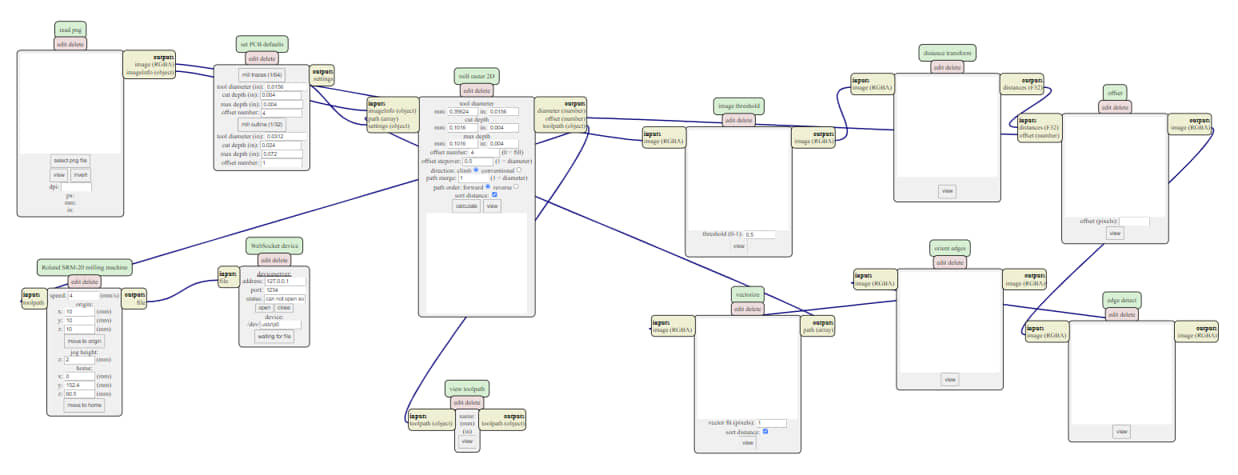
- Add the modul for save file (Right click - Modules - Open Server modules - file -Save; Connect the file to the output file of program)
- Insert the png trace file; change/select the tool diameter with 1/64”, origin of machine is x0,y0,z0
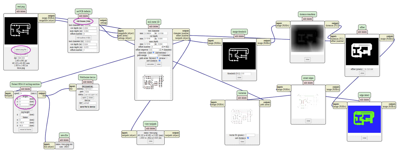
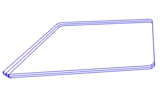
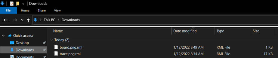
- Calculate, get (download) the file (.rml) and the visualize of path tool
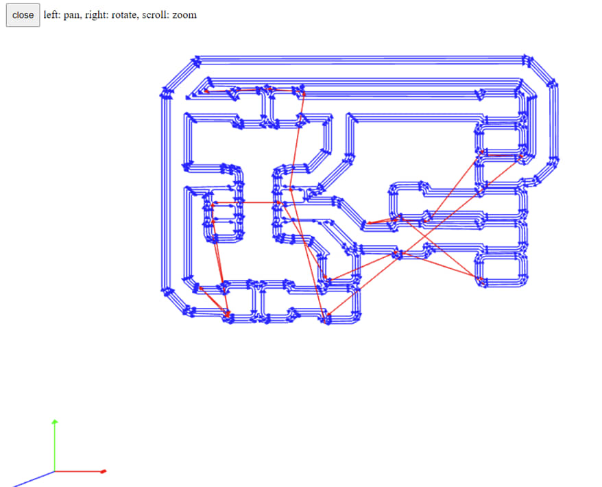
- Do the same proses for “interior”
Note
change the tool diameter for 1/32”
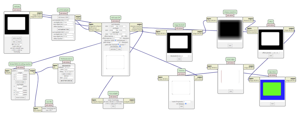
- Get and send the file to the router machine
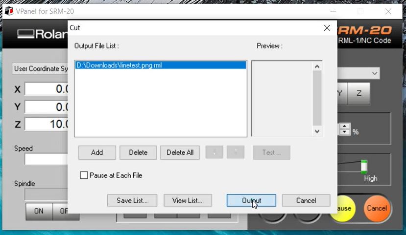
Create the PCB board with SRM-20
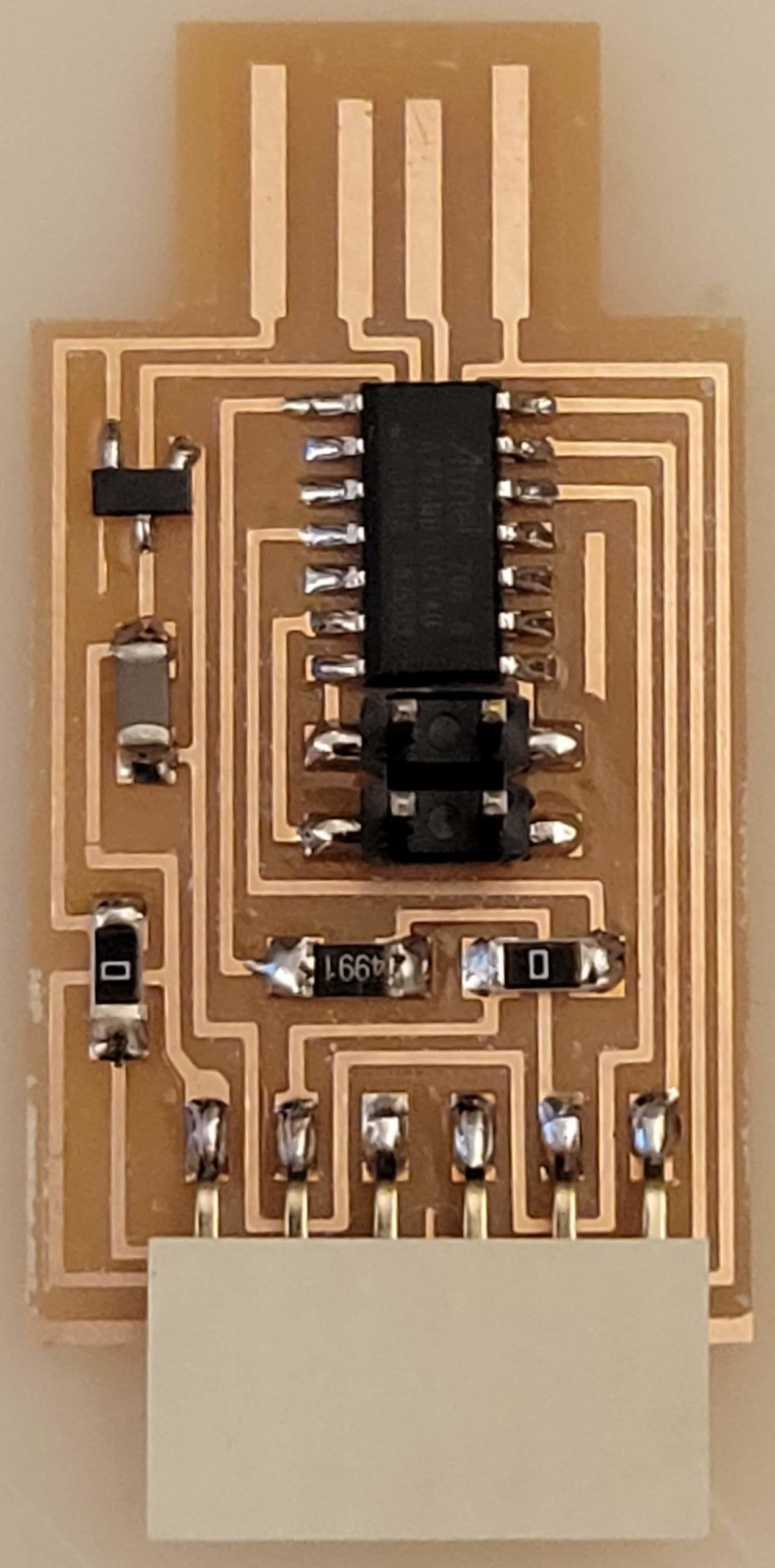
After we get the file look for Mods (rml files). we use the file to cut the PCB board. I used PCB FR1, I put it on a wooden base on the SRM machine (I used a double tip to attach the PCB board to the wood)
The steps taken are the same as in the Group Assessment
- Setting the datum (zero position) for x, y, and z,
- Position (elevate at z-axis) cutter in a safe position,
- Load the rml files (on the cut menu), then press “output”
PCB Milling
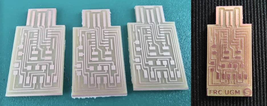
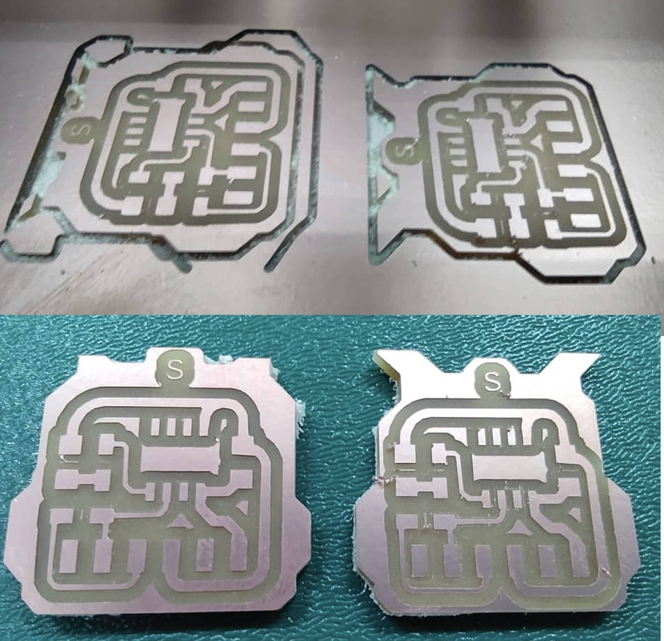
When making the ATTiny 412 PCB, I tried to modify the interior (board shape) to make it look attractive. I tried to add a polygon (eagle-board) outside the board that had previously been made interior, then I exported it in png, made G code with Mods, and Milled it as usual (there are several polygons to make the PCB interior shape). It turns out that the path for the interior follows each polygon route, not just based on image shape in the png, so that in the first process there are parts that are truncated. So that the next correction I made the interior by making only one polygon following the shape to be made, while the image from the previous polygon had to be deleted. The first process is shown in the image on the left, while the repair is in the image on the right
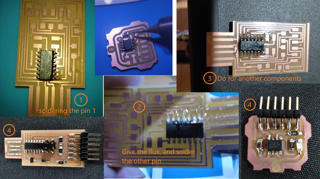
Soldering the components
Before installing the components, there are several equipment that must be prepared such as: - Soldering stations - Fume extractor - Magnifying glass - Tweezers - Soldering mat - Component adhesive - Tin 0.3 mm and 0.6 mm - Solder flux, etc.
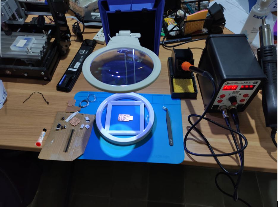
Soldering steps:
- attach the PCB board to the soldering mat, if necessary, stick it so that the PCB does not move. The solder mat is usually rough, so it’s usually enough to keep the PCB board from moving.
- to install smd components (eg IC), give just a little lead on one of the copper lines, the point is to hold when the soldering IC does not move. Pair the IC and solder/melt the lead on the IC pin to hold the IC.
Apply solder flux to the copper pins and tracks for easy soldering.
Soldering IC feet, there are 2 ways:
- heat the IC pin contacts and copper lines, give a little lead and tire it out until the lead is perfectly attached to the IC pin contacts. Use a pointed soldering tip. do for each IC pin.
- give a lot of lead to all the IC pins, heat it up to make sure all the pins are attached to the PCB line. Drop residual tin using tin gravity, or using weak soldering tape for tin removal
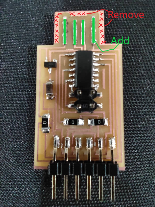
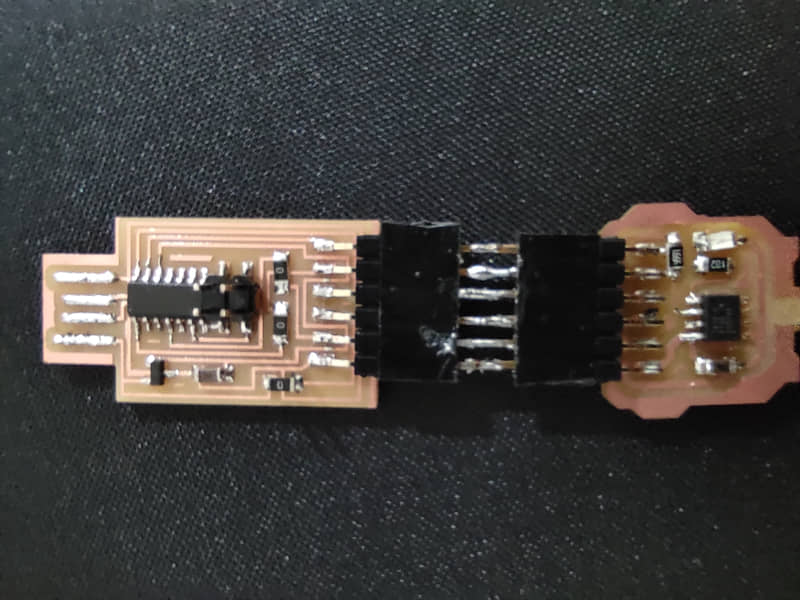
After the components are finished, to connect between the programmer and the minimum system ATTINY 412, make a jamper from a 6 pin black housing.
To ensure a USB connection, tin is added to the connector for USB to thicken the layer and remove the remaining copper lines on the outside.
Programming the PCB
UPDI Programmer (Burn Bootloader to SAMD11C)
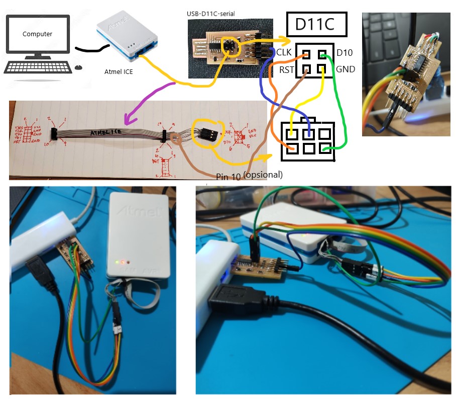
So that SAMD11C can be used for programming, we need to first upload the boatloader to SAMD11C. The tool needed to burn a boatloader is an Atmel ICE.

We need to connect ATMEL ICE with USB-D11C-serial. the default cable does not match the pins on the D11C so we need to modify it.
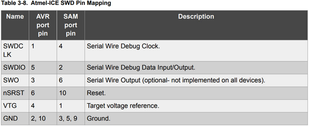
(image source: Atmel-ICE User Guide)
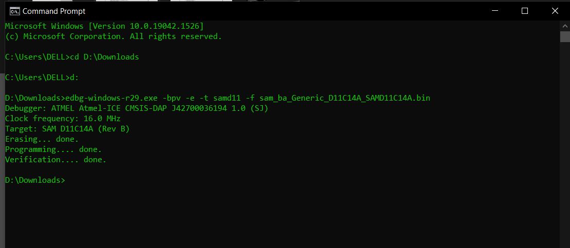
We need to burn a bootloader to enables our board to work with an Arduino sketch The bootloader can download here We also need the edbg to burn to D11C. Edbg can download here
run this command
edbg-windows-r29.exe -bpv -e -t samd11 -f sam_ba_Generic_D11C14A_SAMD11C14A.bin
If successful, the window will look like this:
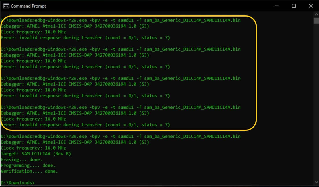
If you got this error, please check the connections
Sometimes when connected to a USB (computer) “USB not recognized” occurs, this happens because the USB end connection is not good. so the alternative is to add a USB male connector
Install Core
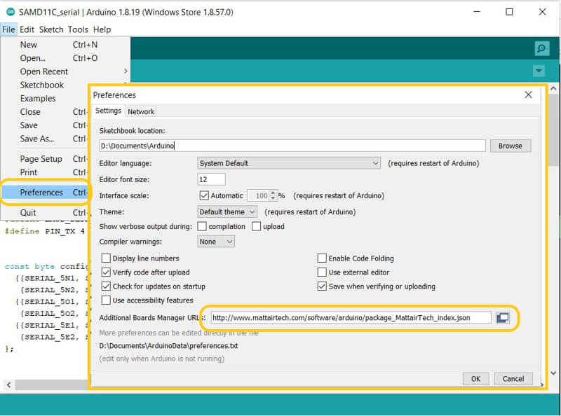
After programming a bootloader successfully, we have to install the board package, so-called, core, for ATSAMD11C (before uploading an Arduino sketch). - Open Arduino > preferences; Add following URL to Additional Boards Manager URLs section
http://www.mattairtech.com/software/arduino/package_MattairTech_index.json
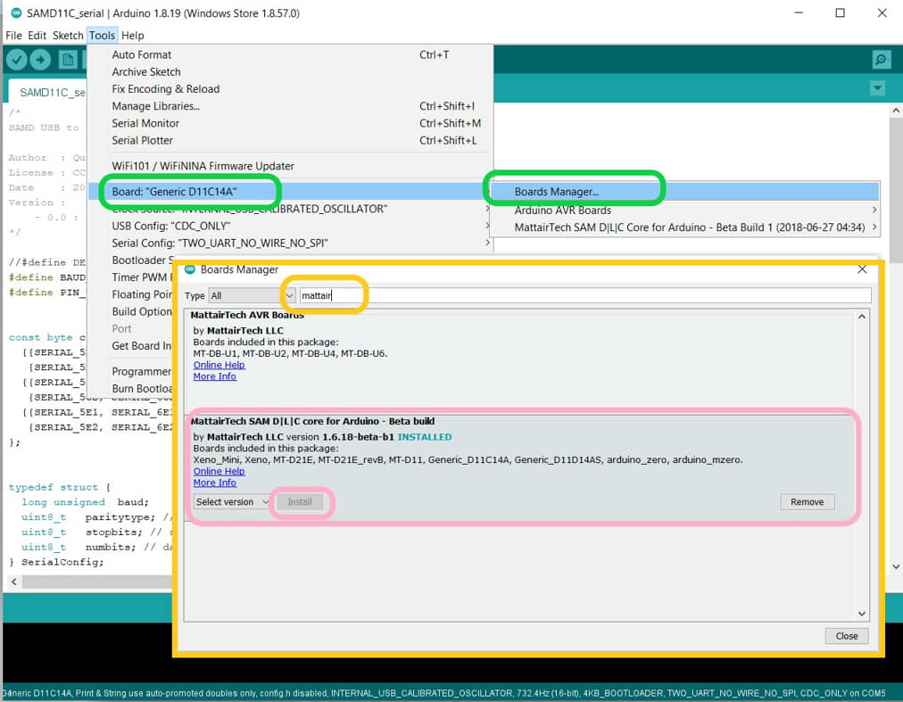
- install MattaireTech SAM D|L|C core
Go Tools > Board > Board Managers, search mattair and install MattaireTech SAM D|L|C core for Arduino.
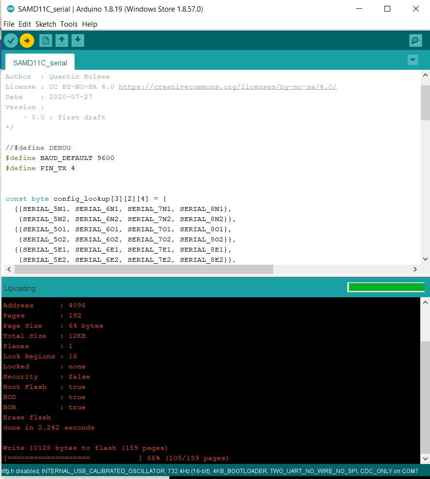
Upload sketch (ArduinoIDE to SAMD11C board)
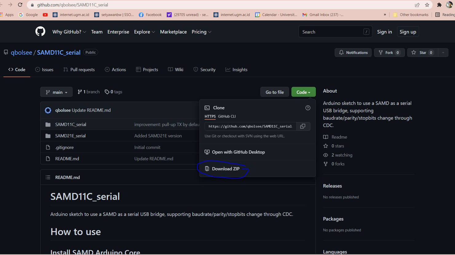
- Download a sketch SAMD11C_serial.ino, and uncompressed it and open (SAMD11C_serial.ino) with Arduino IDE.
- Connect the USB Programmer to USB port at the computer.
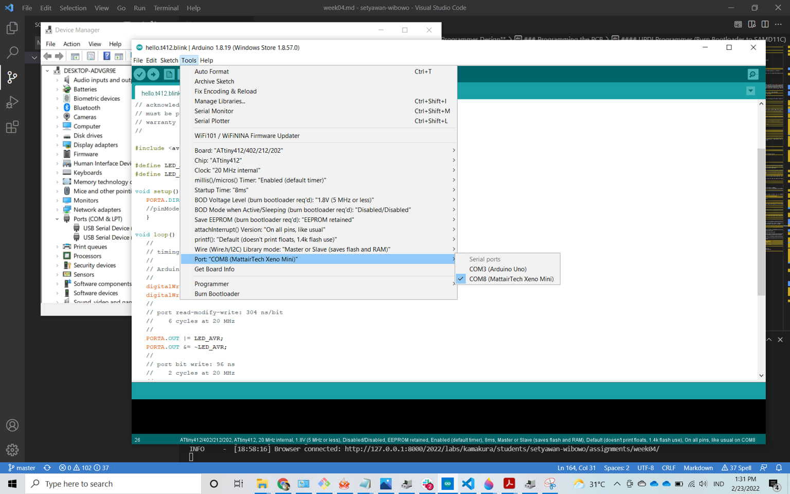
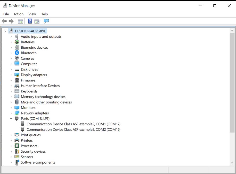
- Cek the port connection (cek with device manager)
-
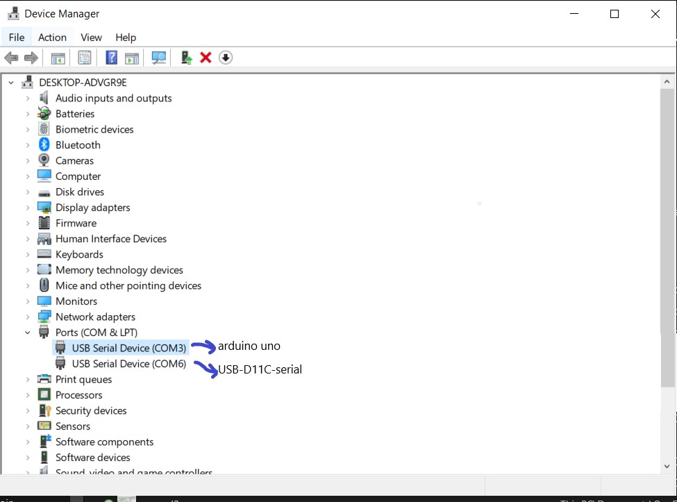
-
Go Tools > Board. Select Board, Microcontrollers, and others as an image shown below. Then, upload the sketch.
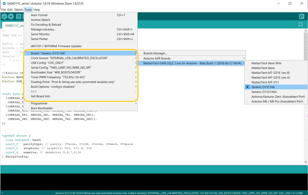
then upload
Upload the program to ATtiny412
This time we will try to program “blink” to test the ATTINY412 board.
- Download the program hello.t412.blink.ino, than open it with Arduino IDE.
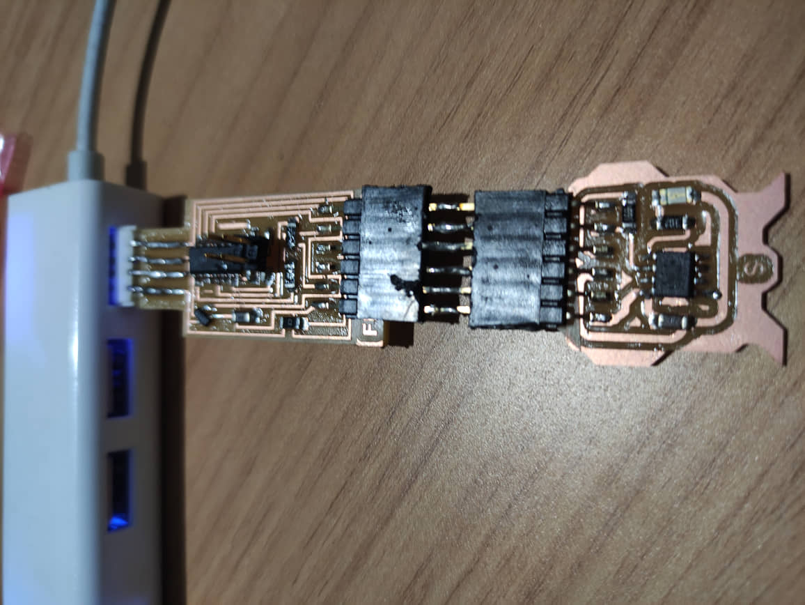
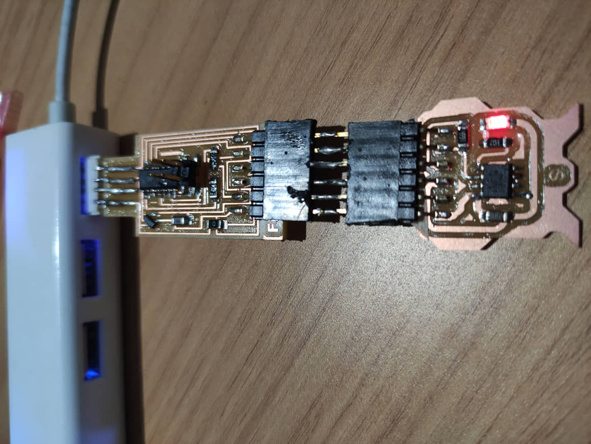
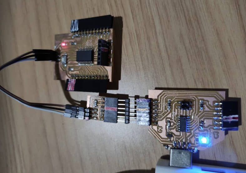
- Connect the computer, USB-D11C-serial, and hello.t412.blink board (Use an USB extension cable or USB Hub for USB-D11C-serial connection to the computer so as not to damage the computer if the board and solder sizes don’t fit right)
then upload
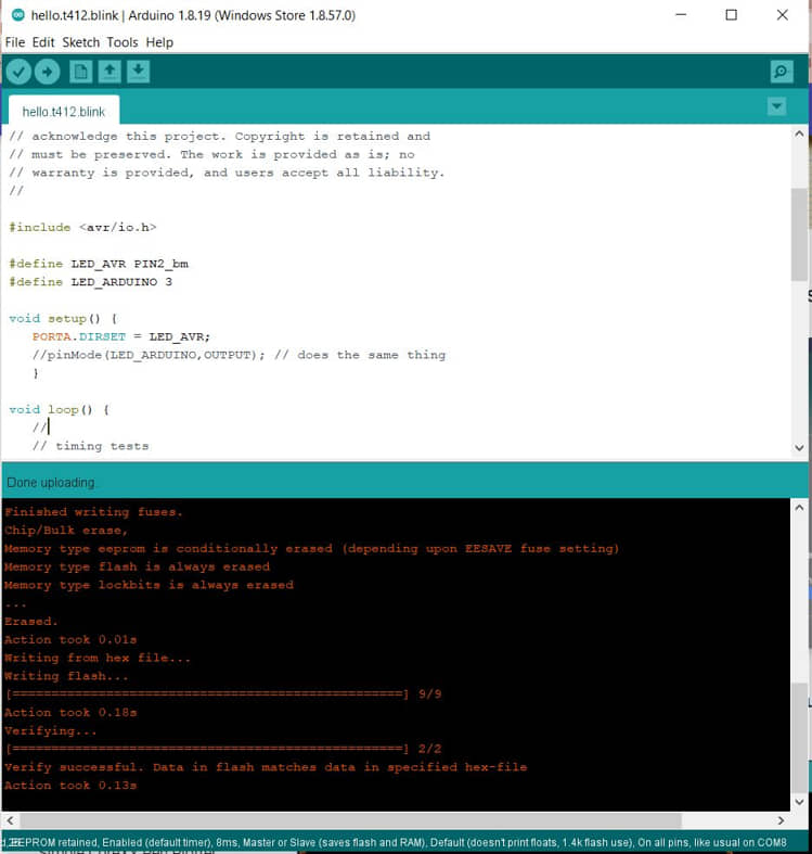
and We GOT
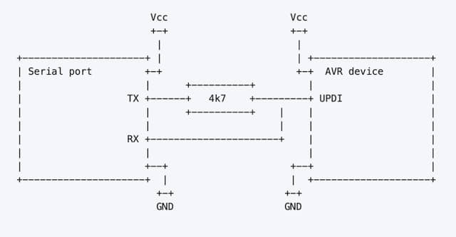
At first discussion with the group, we replaced 4k9 resistor with 0 ohm. we thought it was a resistor on the TX-UPDI track. We want to make it a USB Serial Bridge too. Even though it can and does work, it doesn’t seem right, from the UPDI diagram it takes a resistor. So I will return/fix the value of R 0 ohms to 4k7.
SAMD11C Dual Serial
In Week 8 (Embedded programming) and Week 10 (Output Device), I felt that I need two SAMD11C USBs that I have made to simultaneously be used as an UPDI programmer and Serial comunication. If you use one SAMD11C board, sometimes it’s quite complicated because you have to remove and install it when the serial position or UPDI programmer is in, so I made two PCBs that can be used at once.
When I heard Neil that at Fab Academy Quentin Bolsee made a SAMD11C board that can be used for two functions at once, I was interested in making one too. This is the schematic and board that I made
We need to burn a bootloader to enables our board to work with an Arduino sketch. To download the compiled binary: dual_cdc_d11.bin.
command for edbg :
edbg-windows-r29.exe -bpv -e -t samd11 -f dual_cdc_d11.bin
check the device manager :
testing for programmer :
Tests for dual serial use will be presented at the end of week 6 (Electronic Production)
References
- Kamakura : Electronics Production : Local Session
- SAMD11C Development Board
- Kamakura : FA2022/Electronics Production
- Kamakura : FA2022/Computer Controlled Cutting
- Kamakura : USB-D11C-serial#
- tinyAVR 1-series
- Kannai : Burn Bootloader to SAMD11C with Microchip Studio (Windows)
- Kannai : FA2022 Embedded Programming Environment
- ATMEL-ICE
- SAMD11c dual serial
Documentation Files
- Inkscape modification USB-D11C-serial (.svg)
- Modification USB-D11C-serial (.png)
- Modification USB-D11C-serial-interior (.png)
- Modification ATTINY412 (.png)
- Modification ATTINY412-interior (.png)
- hello.t412.blink.ino
- SAMD11C boatloader
- SAMD11C dual_cdc_d11.bin
Lessons learned (week 4 : Electronics production) :
- Applying how make the schematic to PCB production
- Applying how to make mods to get the CAM files to PCB CNC Production
- Applying the procedure to operate the CNC Mini router for PCB productions
- Applying soldering the smd components to the board
- Applying upload the PCB Programmer