14. Networking and Communications
The plan
I’ll try to use this week to prepare for the final assignment. The plan is to:
-
Create a I²C master, which might be used as the main controller in the final project.
-
Create a I²C slave that might implement functionality for the final project such as a button/led board that speaks to the bus.
For this week I’ll be using ATtiny1614 microcontrollers for the boards.
The master
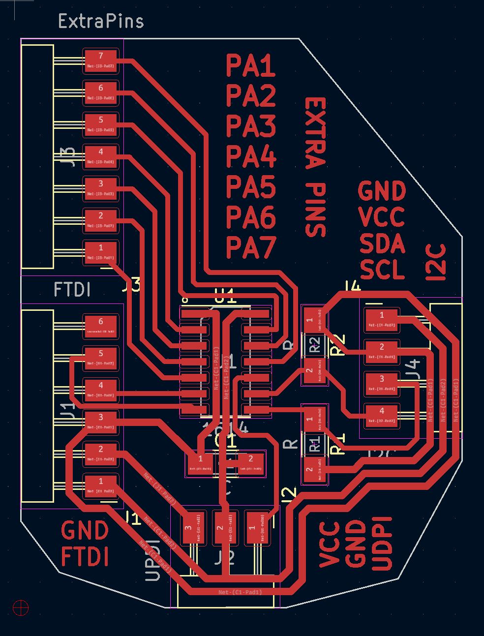
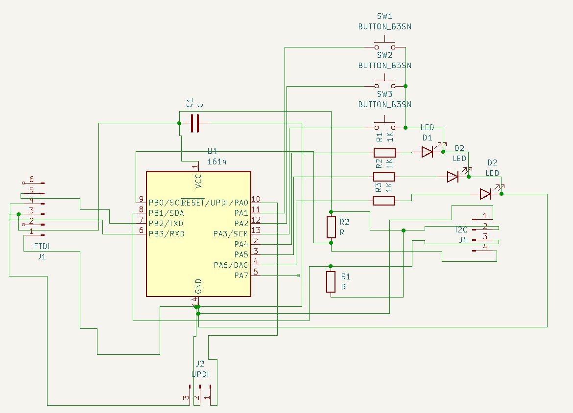
Using KiCad I create a board for the microcontroller. Main focus is to add connectors for all the pins, so that I cas use the chip to prototype as much as possible.
Update
Before starting KiCad, I make sure to update the wonderful FabLab KiCad library.
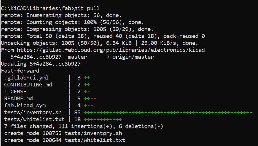
Fun fact: I updated it recently, and it still fetched updates. It’s so nice that it’s being actively updated.
Design the board
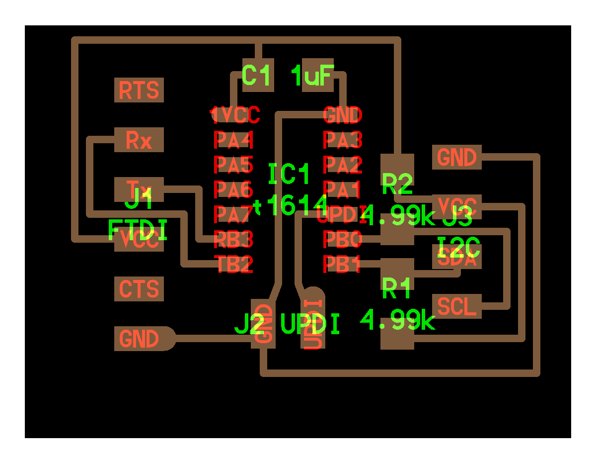
I use the hello I²C t1614 board from FabAcademy as a reference.
In KiCad I start by creating a new project.
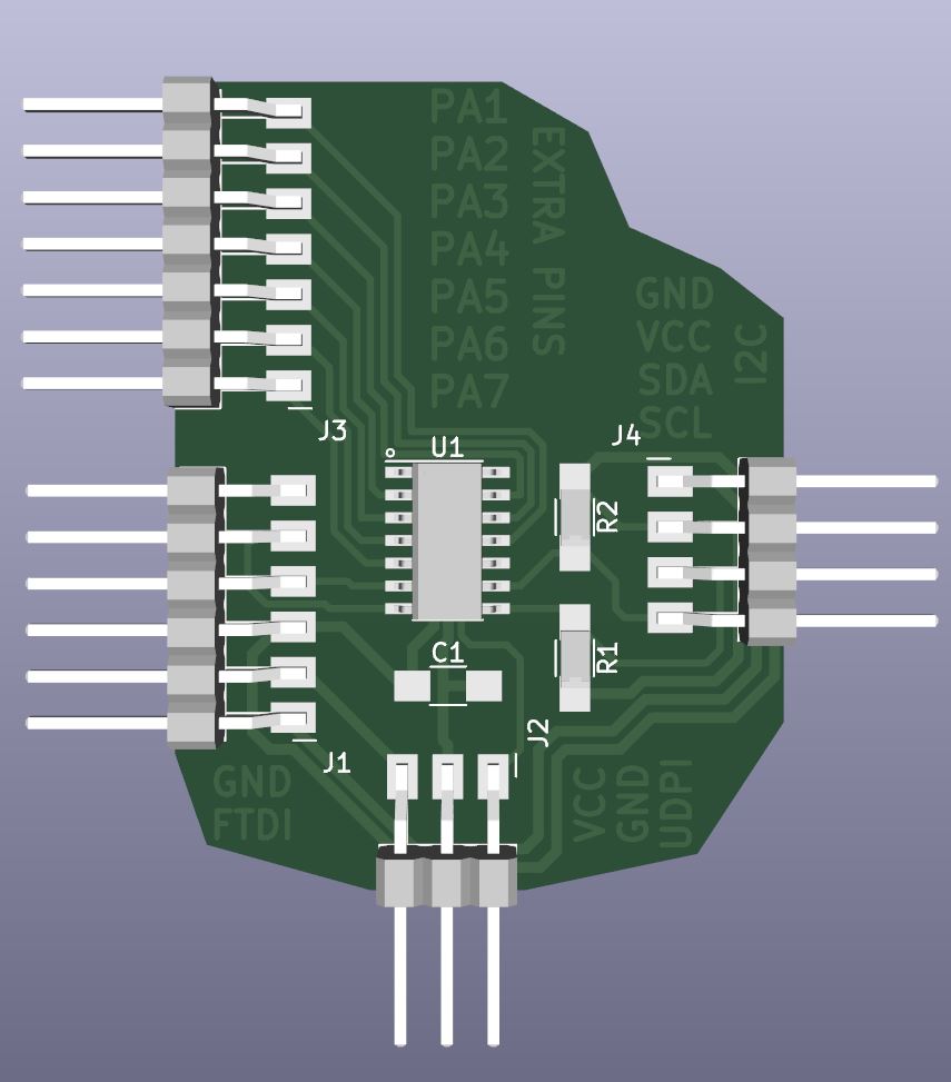
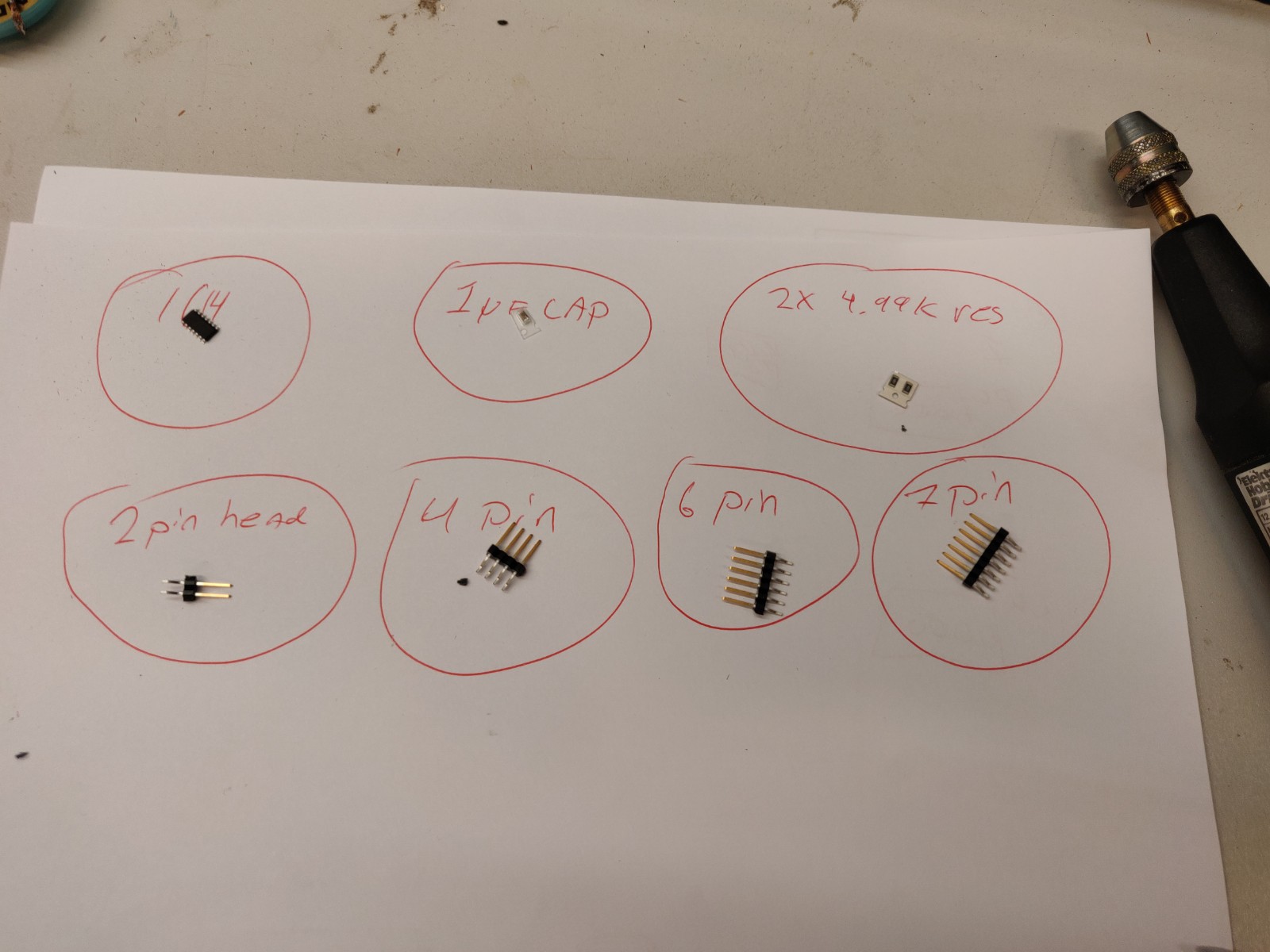
In the schematic editor, I add the components needed for the board. I use the ones displayed in the image above, with an additional 7 pin header connector. All components are SMD and are in the library mentioned above.
| Volume | Components |
|---|---|
| 1 | ATtiny 1614 |
| 1 | 1μf capacitor |
| 2 | 4.99k resistor |
| 1 | 3 pin header |
| 1 | 4 pin header |
| 1 | 6 pin header |
| 1 | 7 pin header |
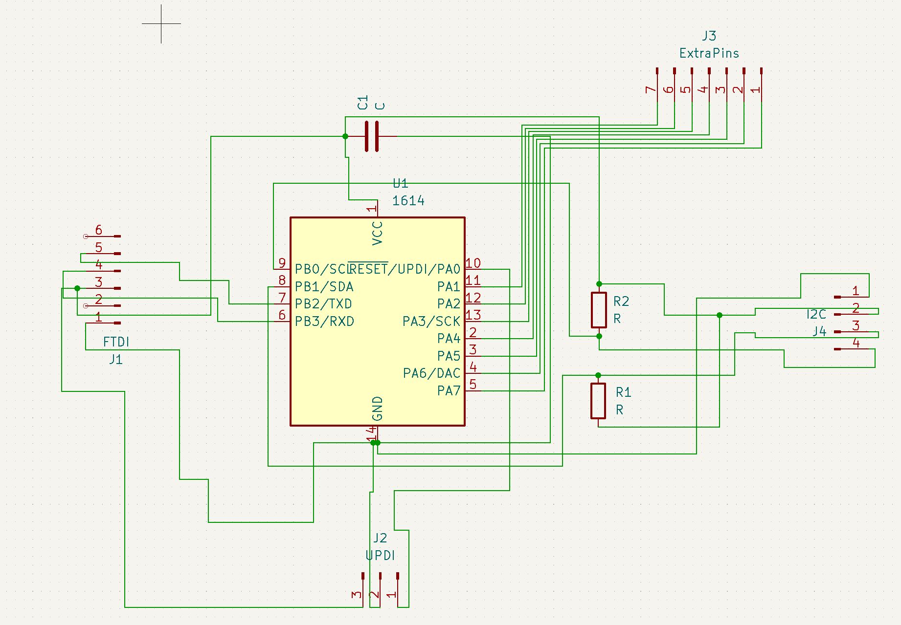
Schematic
I start by connecting the components the same way as the board layout above and then add the 7 pin connector.
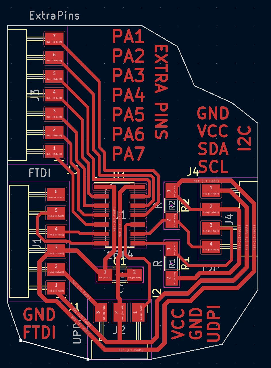
PCB Layout
As always, it takes me a bit to organize the components and I need practice with this if I’m to be proficient with electronics design.
But I managed to arrange the components so that I don’t need any jumpers and I hope this is not considered horribly messy.
mm vs mils
One thing to note, is that it took me a while to realize where I switch from mils, which is 0.001 of an inch, to millimeters! The imperial system is not my cup of tea.
In board editor, I set two track widths. 0.6 mm for VCC and GND lines and 0.4 mm for the rest of the lines. Hopefully that will be sufficient and the milling goes well.
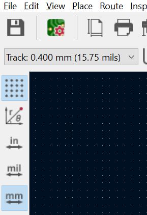
The shortcuts are located on the top left, just below the save and board setup icon.
3D View
I really like this feature in KiCad, that I can view a 3D view of the board. It’s only missing the capacitor for some reason.
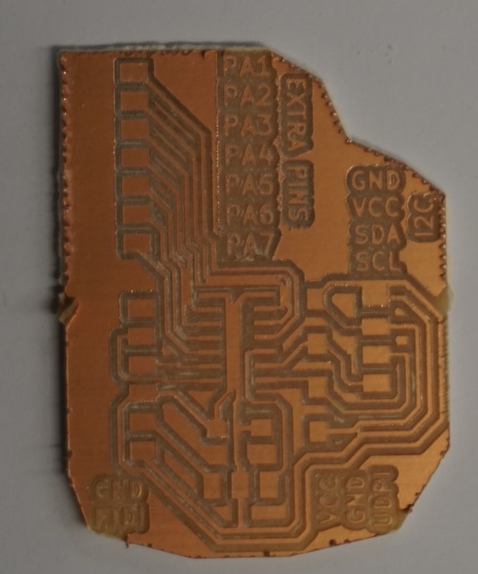
Like in the last board I made, add a bit of identifcations to the pins to minimize confusion later on.
Finalize for production
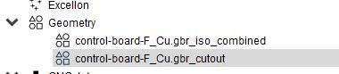
Last thing I do in KiCad is to export the Gerber files to use in FlatCAM.
I go to File -> Fabrication outputs -> Gerbers. In the dialog there, I start by unselecting all layers except for the front copper layer (F.cU) and the Edge cuts layer.
Additionally, I select the Use drill/place file origin since I had placed a origin point in the lower left corner of the board design.
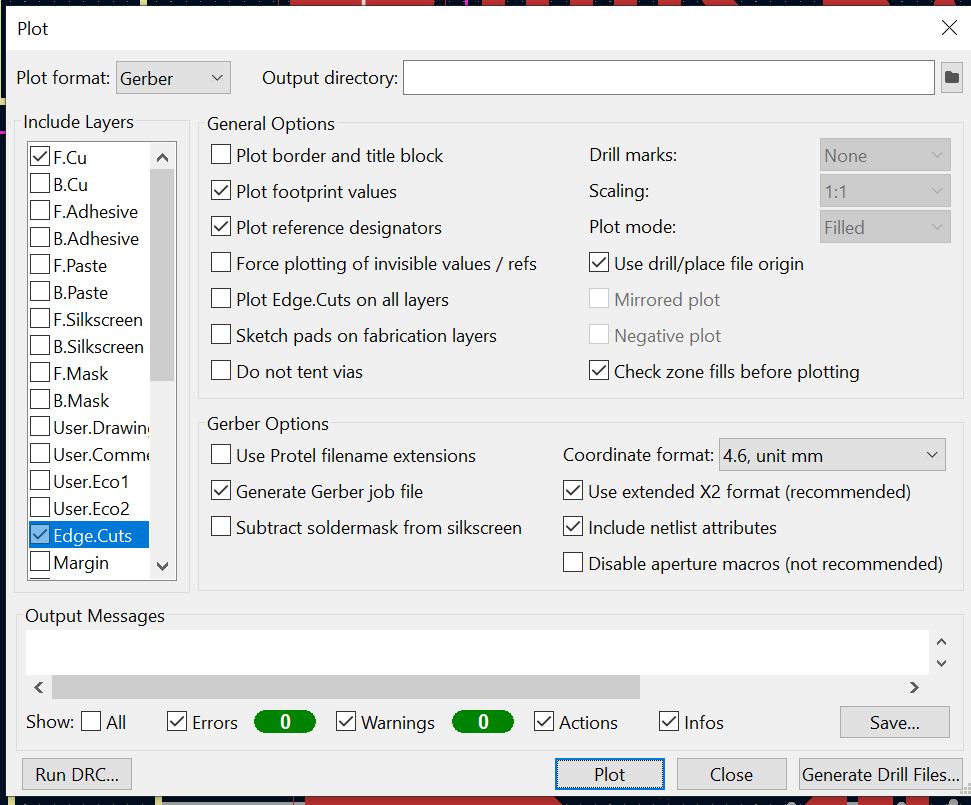
I select Plot and thats that! I now have two Gerber files in the project folder.
Milling
FlatCAM
F.Cu
In FlatCAM (V 8.994) I start by loading the both Gerber files, File -> Open -> Gerbers.
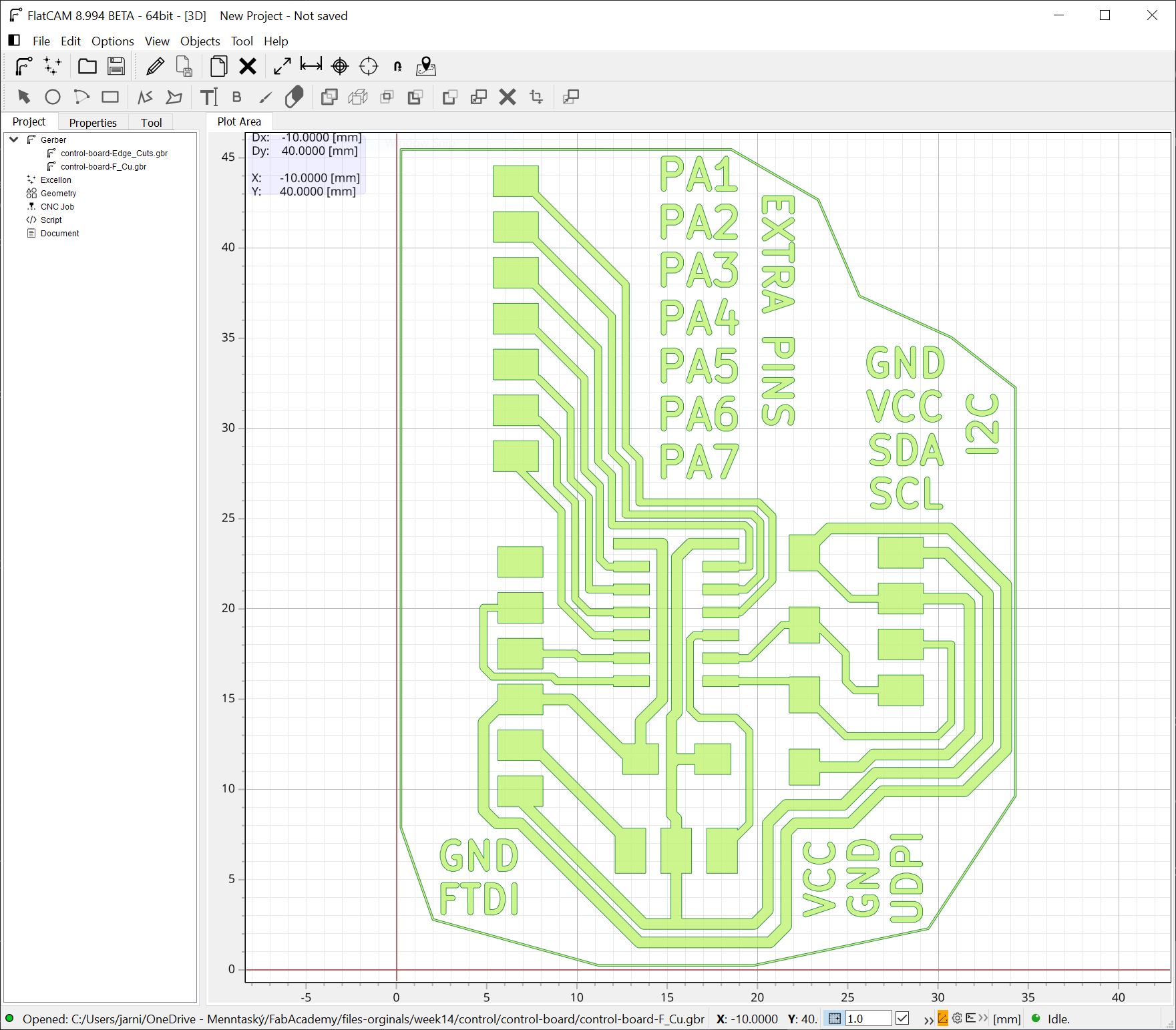
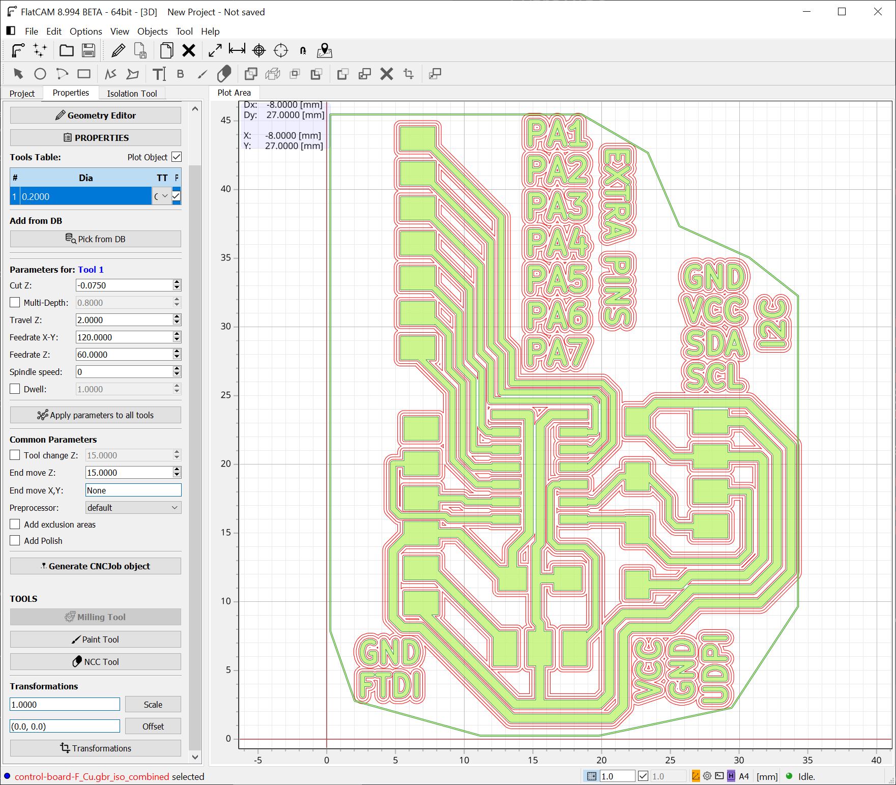
I start by prepering the F.Cu, by clicking the F.Cu file under Gerber in the left menu. In the next menu, I select Isolation routing.
As before, I select my milling tool from the DataBase. For reference, it is a 0.2 diameter Vbit, set to mill Z height of: -0.075mm.
Once loaded, I select Generate Geometry and am presented with this view:
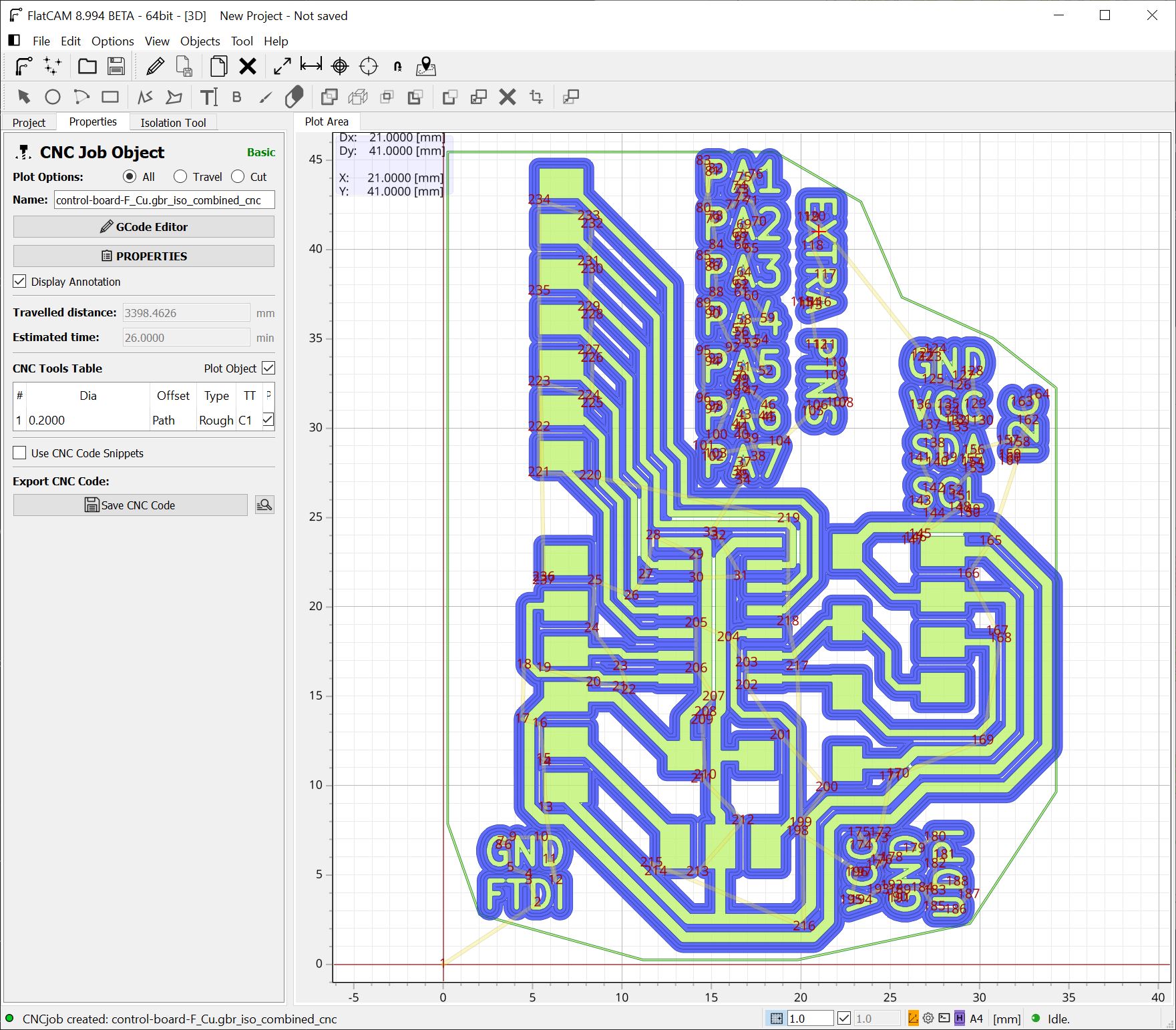
Finally I select Generate CNC object and I get this view, where I select Save CNC Code:
Edge cuts
I return to the main view and select the edge cuts Gerber file. There I select Cutout Tool, where I’m presented with this view:
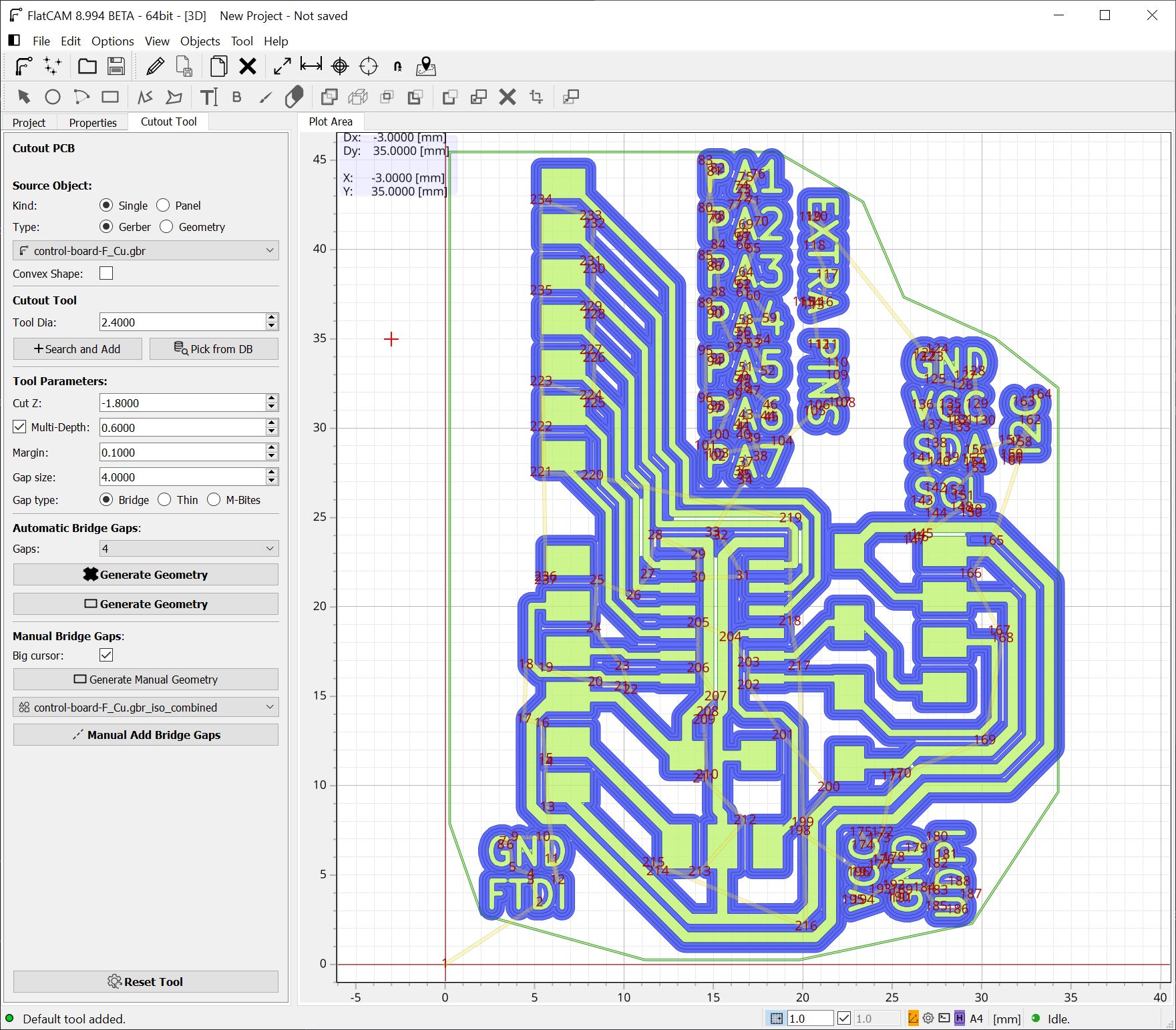
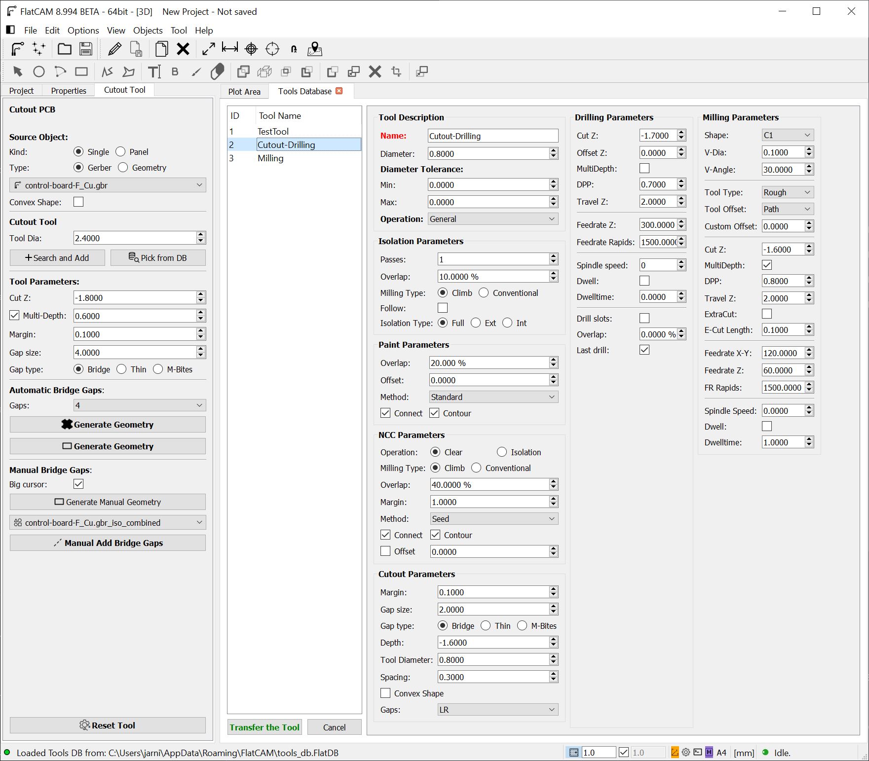
I remove the default tool select my Cutout-Drilling tool from the database.
Once loaded, I select the Generate Geometry with the X (irregular) shaped icon and I get this view:

I must now return to the main menu and select the cutout geometry object.
Once there, I select Generate CNC object and again I select Save CNC Code.
CNC-ing
Yet again, I’ll be using our Wegstr machine.
I add a FR4 plate to the bed, open the software and position the drill to where I want to start. There I zero the X,Y position.
Next I lower it until it makes contact and I zero the Z axis.
TODO: Mynd af WEGSTR forriti
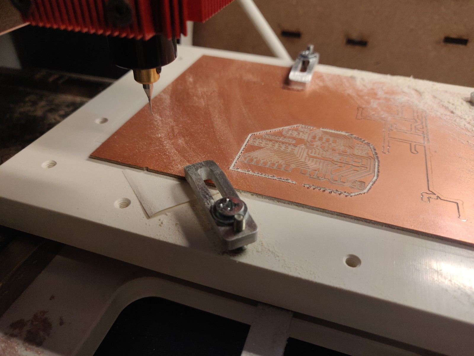
I load the F.Cu file and start milling.
A bit of trouble
It started well, then the milling kind of faded away, like the bit was not touching.
First I tried to add a bit of depth to the Z axis, simply by opening the .nc file and search && replace -0.075 with -0.1. This saved me the trouble of going back to my computer and going through the FlatCAM steps again.
Sadly, that was not enough, it happened again. Next thing I did was zero the positions again, but nearer the CNC bed center.
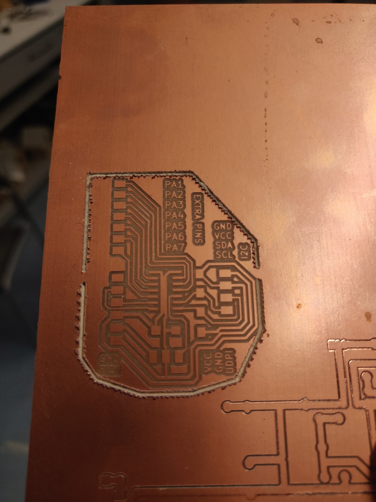
It went better this time, but not all traces were good. I tried to clean the up a bit by hand, but I was not happy with the result. So I went back to KiCad, adjusted the tracks and created a bit more space in between the them.
I then redid the steps in FlatCAM and milled again.
Second try
Then I moved on to the edge cuts. After replacing the tool with the Cutout-Drilling tool, I zero the Z axis, load the edge cuts file and start milling.
This went better, although there were two things that went wrong. There were still slight mistakes with the traces, which I managed to correct manually.
Also, when milling, the top left corner (near a mounting clamp) was “faded out”. Like it was over-tightened. But I know I did not do that, so I’m starting to suspect that the milling board is misformed. What I did was to undo that clamp, slide a piece of paper under neath the board and it finished perfectly!
Soldering
Soldering is fun!
I find the parts, setup the station and start soldering. That went well.
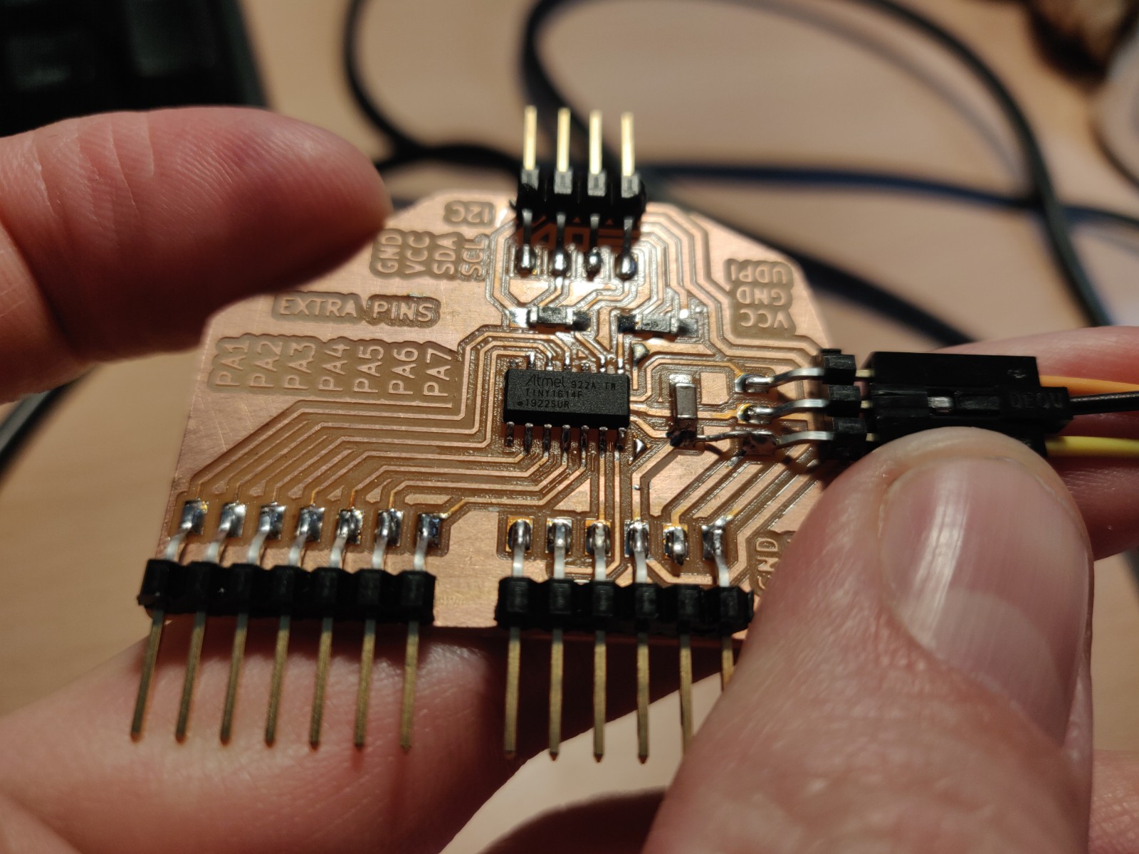
Although, once I had finished and plugged it in it did not work. Turned out I had gotten a bit confused and misplaced a VCC connection. I fixed that with a jumper and removed the wrong pin connector, on the FTDI connector. I updated the KiCad project accordingly.
Programming
Arduino
To test if I could get I²C working on my board, I want to use an Arduino Nano as a testing board. I will consider this as the “group project”, as in my board speaking to another project and I am by myself.
Looking at the Arduino docs I found the following.
I will be using the Arduino nano as the reader and my board as the writer. This makes sense in two ways, as I hope to use mine as the writer/master/commander board and the Nano has a built in LED to turn on so the default testing code should suffice.
I²C Reader
This is the code I upload to the Arduino Nano:
#include <Arduino.h>
#include <Wire.h>

void setup() {
  Wire.begin(8);                // join I²C bus with address #8
  Wire.onReceive(receiveEvent); // function that executes whenever data is received from writer
}

void receiveEvent(int howMany) {
  char c = Wire.read(); // receive a character
  if(c == '0'){
    digitalWrite(LED_BUILTIN, LOW);   // turn the LED off by making the voltage LOW
  }
  if(c == '1'){
    digitalWrite(LED_BUILTIN, HIGH);  // turn the LED on (HIGH is the voltage level)
  }
}

void loop() {
}
It monitors the bus and watches out for messages containing either ‘0’ or ‘1’. When it receives a ‘0’ it turns the LED off, and when it receives a ‘1’ it turns the LED on.
My board
This is then what I upload to my board.
I²C Writer
#include <Wire.h>

void setup() {
  Serial.begin(9600);
  while (!Serial);
  Wire.begin(); // join I²C bus (address optional for writer)
}

int readSerial(char result[]) {
  int i = 0;
  while (1) {
    while (Serial.available() > 0) {
      char inChar = Serial.read();
      if (inChar == '\n') {
        result[i] = '\0';
        Serial.flush();
        return 0;
      }
      if (inChar != '\r') {
        result[i] = inChar;
        i++;
      }
    }
  }
}

void loop() {
  Serial.print("Enter 0 to turn off led, enter 1 to turn it on ");
  char ledVal[0];
  readSerial(ledVal);
  Serial.println(ledVal);
  Wire.beginTransmission(8); // transmit to device #8
  Wire.write(ledVal);        // sends the given value
  Wire.endTransmission();    // stop transmitting
  delay(500);
}
Testing
I upload both code bits to their respective boards and connect the bus wires like so:
A4 -> SDA
A5 -> SCL
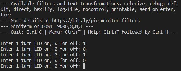
I power on both devices and and turn on the serial monitor for my board.
There I am shown the following option:
14:52:31.331 -> Enter 0 to turn off led, enter 1 to turn it on
If I enter 0 and hit send, the onboard LED turns on. It then turns of if I enter 1 and hit send.
It works!
Moving on!
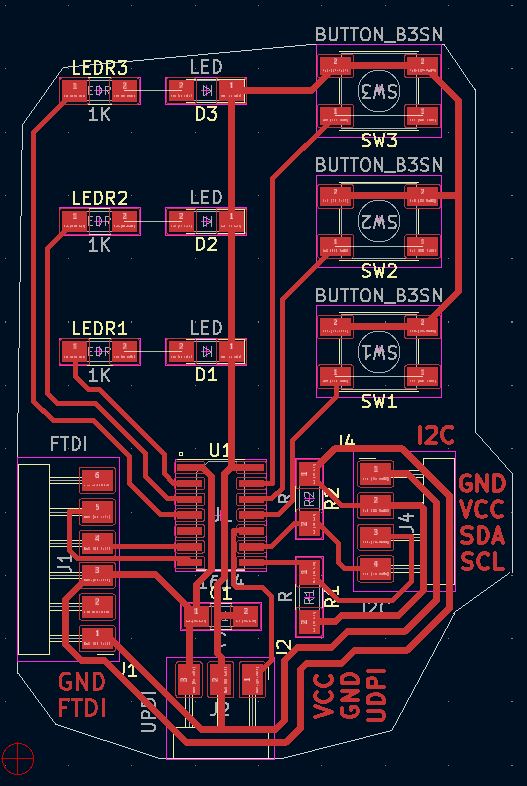
Button board
Next I want to create a board with buttons and LEDs. I’ll start by creating one board, but the idea is that adding another one to the bus would be trivial, one for the parental unit and one for the child unit.
I start by coping the earlier design above, adding the buttons and LEDs to the extra pins.
After spending some time positioning things in the PCB layout, this is what I wound up with.
Troubles!
Improvise, adapt, overcome!
I’m traveling at the moment, on a Fablab bootcamp trip to Ísafjörður. It turned out that the selection of microchips here don’t fit my current needs. Luckily I had brought a box of previously made stuff with me and figured I could turn the board from week07 into a I²C reader!

The board I used has a ATtiny412 chip, a button and a LED. Let’s make do what we have, minimize waste and maximize the fun!
After refreshing my memory of the old board, I adjusted the code so that it would use the LED-pin instead of the built-in-LED. I then set up two new projects in VSCode like before, one for the reader(ATtiny412) and one for the writer(ATtiny1614).
I uploaded the code to each of them, then connected the bus wires between them, along with the VCC and GND wires. Then I connected the FTDI cable to USB and opened up the serial monitor.
VOILA! I’m presented with the option to enter 1 or 0 to turn the LED on or off.
And now to see it in action:
| Compression | ||
|---|---|---|
| Original | After | Reduction |
55.95MB |
3.30MB |
-94.11% |
Thanks videosmaller!
Conclusion
I have now managed to get I²C working, with my own writer board connected to both a commercial board (Arduino Nano) and my own (out in the field repurposed) reader board!
Thanks for joining me in this journey!
Files
| Files |
|---|
| Edge cuts gerber file |
| Front copper gerber file |
| KiCad Control Board |
| KiCad Button Board |
| VSCode projects |