5. Electronics production
Week 05
Oh boy, oh boy! This will be interesting.
Previous work
I do not have so much experience in this field but I’m excited about it. A few weeks ago I took some time to get to know our tools and equipment related to making circuit-boards.
I tried out KiCad, FlatCAM and tested out our Wegstr CNC router. We also have a Roland CNC, but it’s been giving us a bit of a hard time lately.
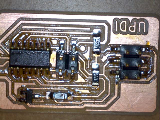
What I did then was to make a ATTiny45 programmer. I only did the cutting and soldering, I did not program it.
Electronics production
This week is not about designing from the ground up, but to make a board from existing designs. My instructor recommended I’d do this board so that is what I did!
KiCad
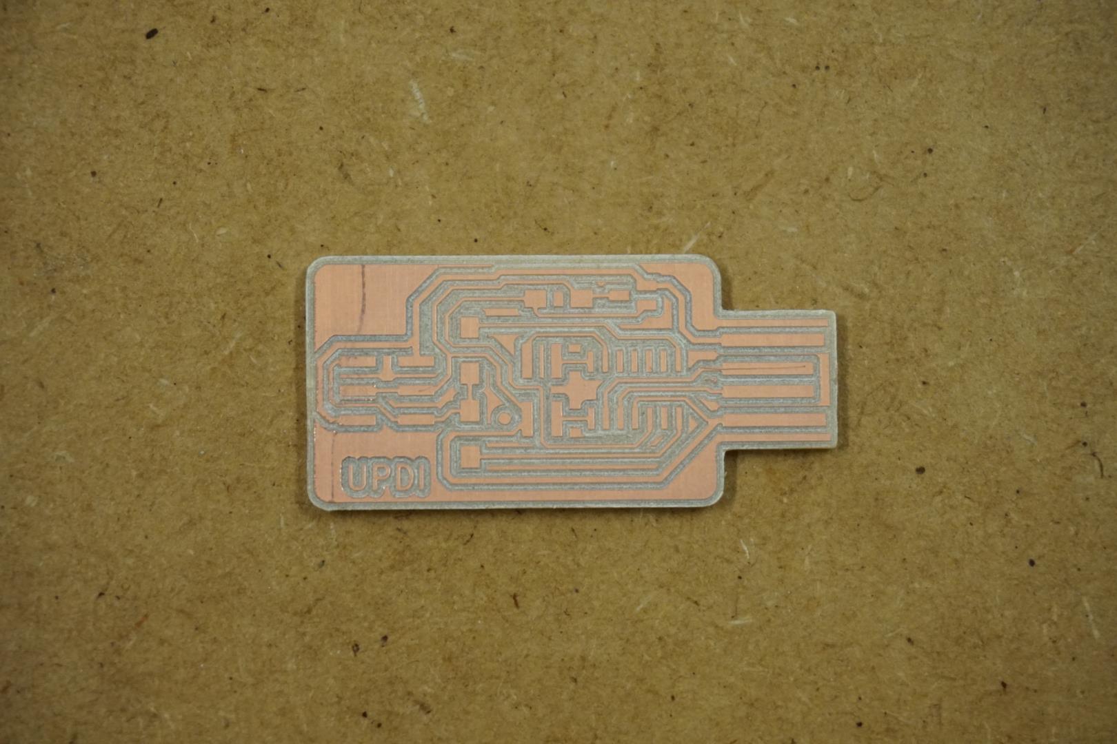
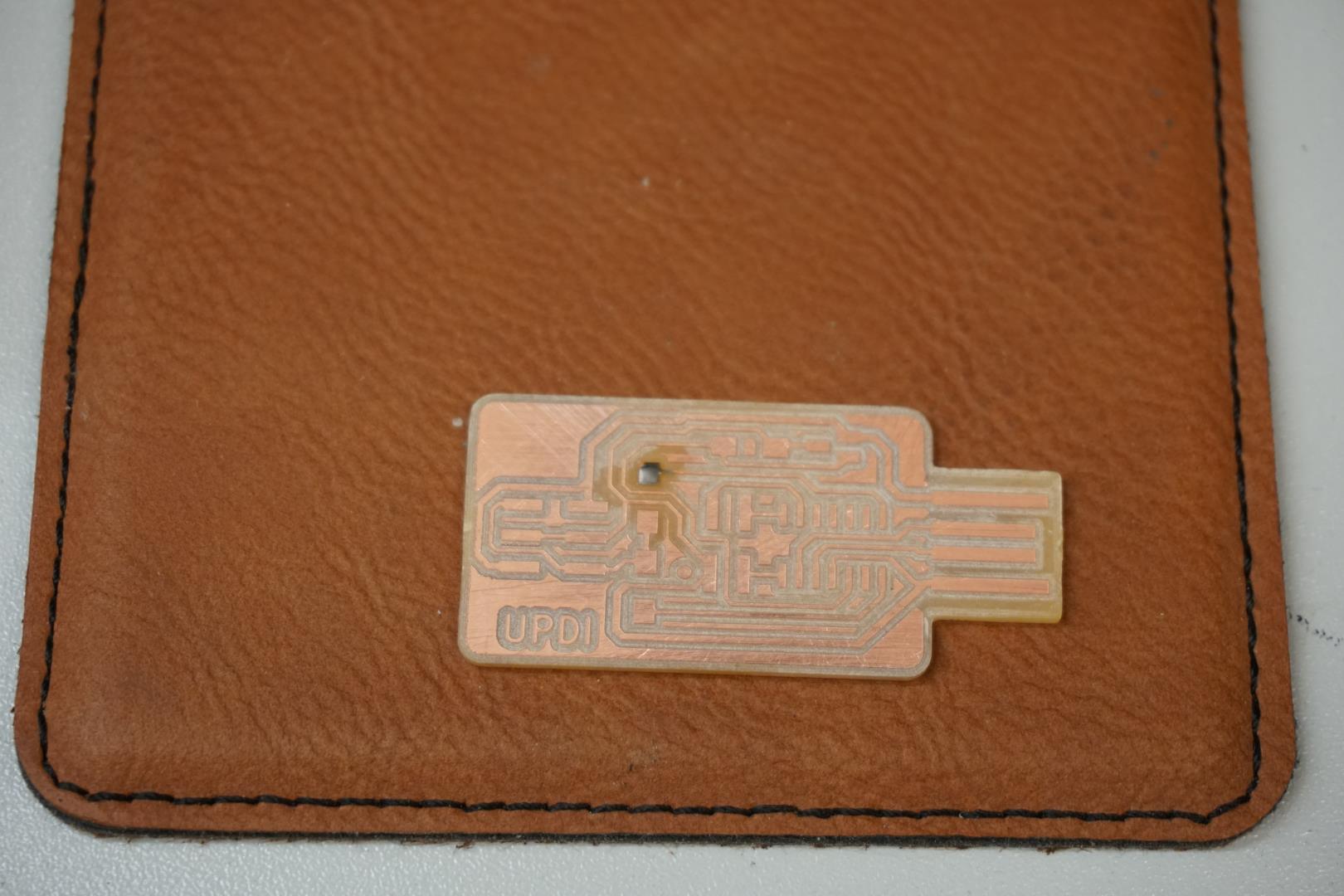
I cloned the repo and opened the project in KiCad. Only thing I did there was to place a new origin point so that I save on material and use scraps to practice. From there I generated new trace files, for the circuit itself and the cutout.
Image files from the project:
| File |
|---|
| Programmer-UPDI-D11C-B_Cu.svg |
| Programmer-UPDI-D11C-F_Cu.svg |
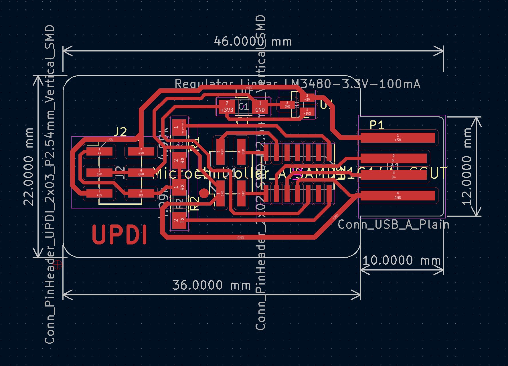
The red circle with the cross is the origin point, lower left part of the image.
FlatCAM
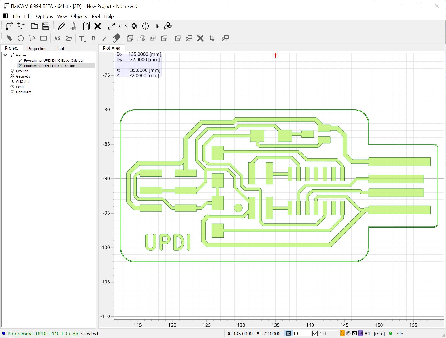
Previously I had gotten to know FlatCAM a little. I decided to try out the 8.994 BETA version. In FlatCAM there is a tool database which I had entered tools for our V-bit and cutout-bit.
The program is pretty unstable and using the database is a bit of a pain. But once the tools are set up, it’s really nice to just select them instead of having to remember where to put what constantly.
I made the CNC objects for milling the traces and the cutout.
First, you load the Gerber files from KiCad. Here I have loaded the FCu and EdgeCut files.
Next I double click the FCu and enter the properties dialog, where I select Isolation routing, which is for the traces. There I can select the tool, which I have already setup in the database. To do this, select the Pick from DB and double click the desired tool.
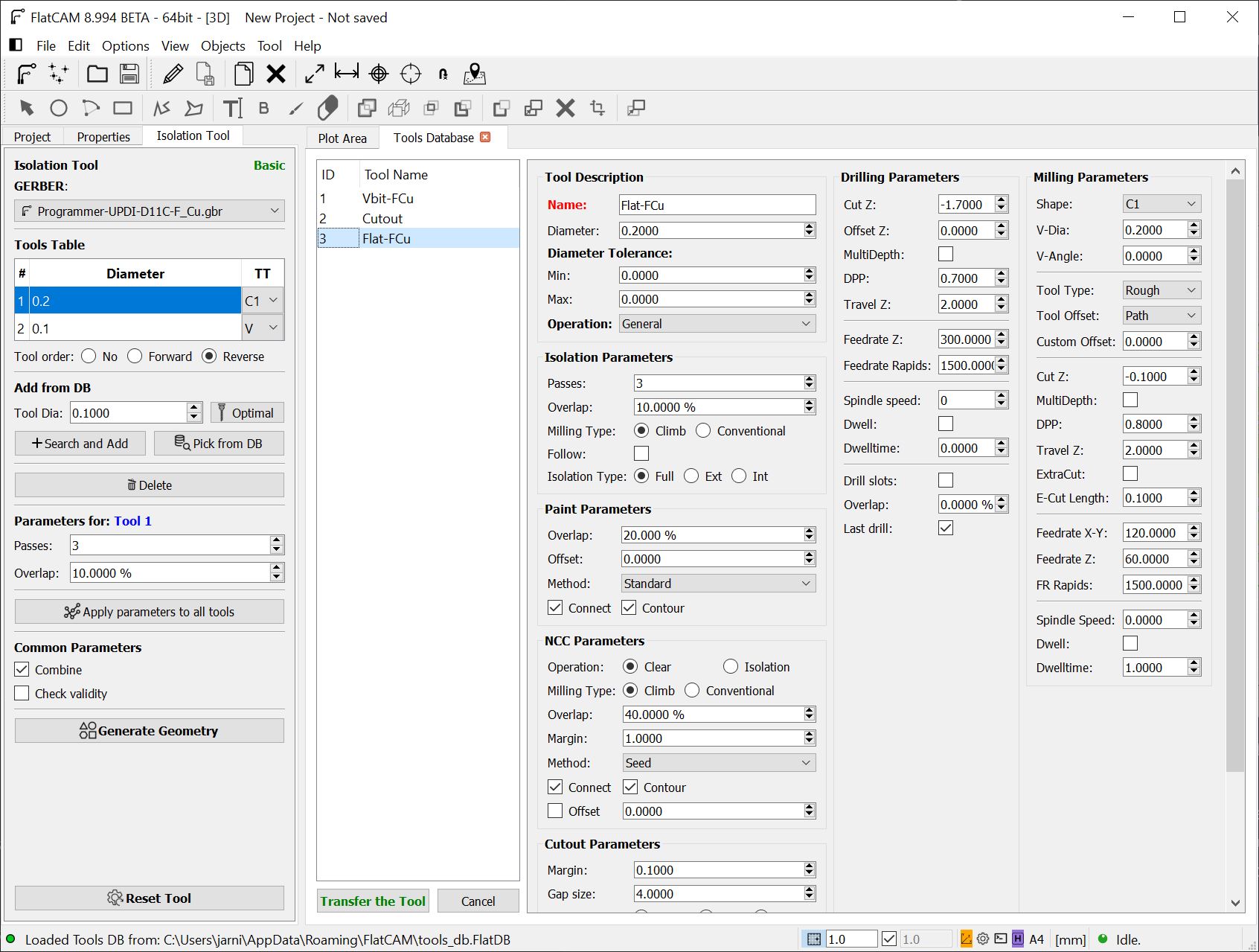
Note, it's rather unstable. Remvoing a previusly selected tool with the `delete` button crashes the program.
Once the tool is selected, you can adjust settings such as passes and overlap. Then you hit the Generate geometry button. This presents you with a visible toolpath.
Here shines the beauty of the tool database. I have already set the cut-depth, the Z travel, feedrates and all that. This feature is brilliant in my opinion.
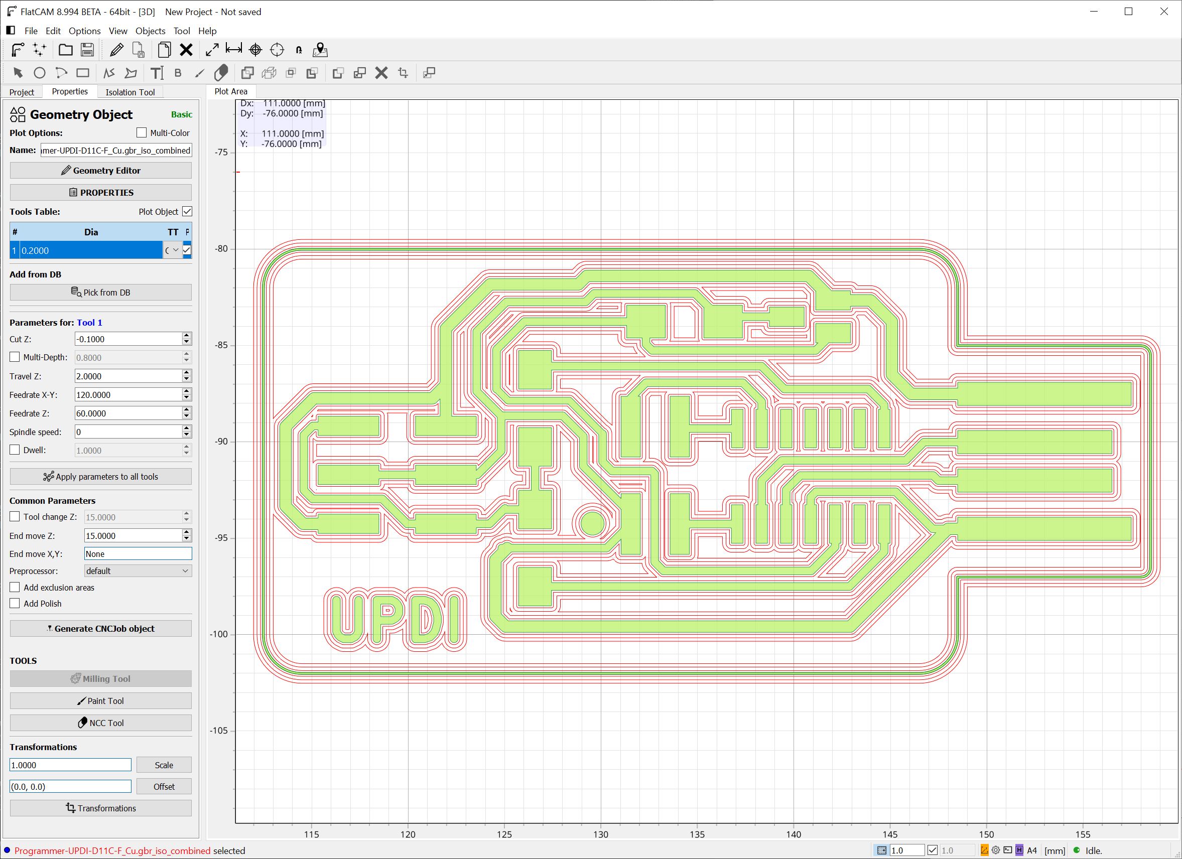
Next is simply to hit Generate CNCJob object and then Save CNC Code to get the .nc code.
You would then repeat this process for the cutout.
Wonderful!
Please note that in week11 I have a further step by step guide to using FlatCAM and the Wegstr CNC router.
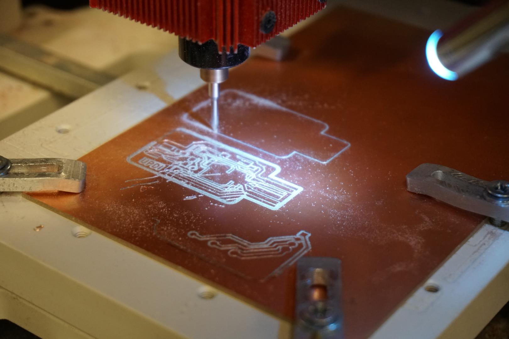
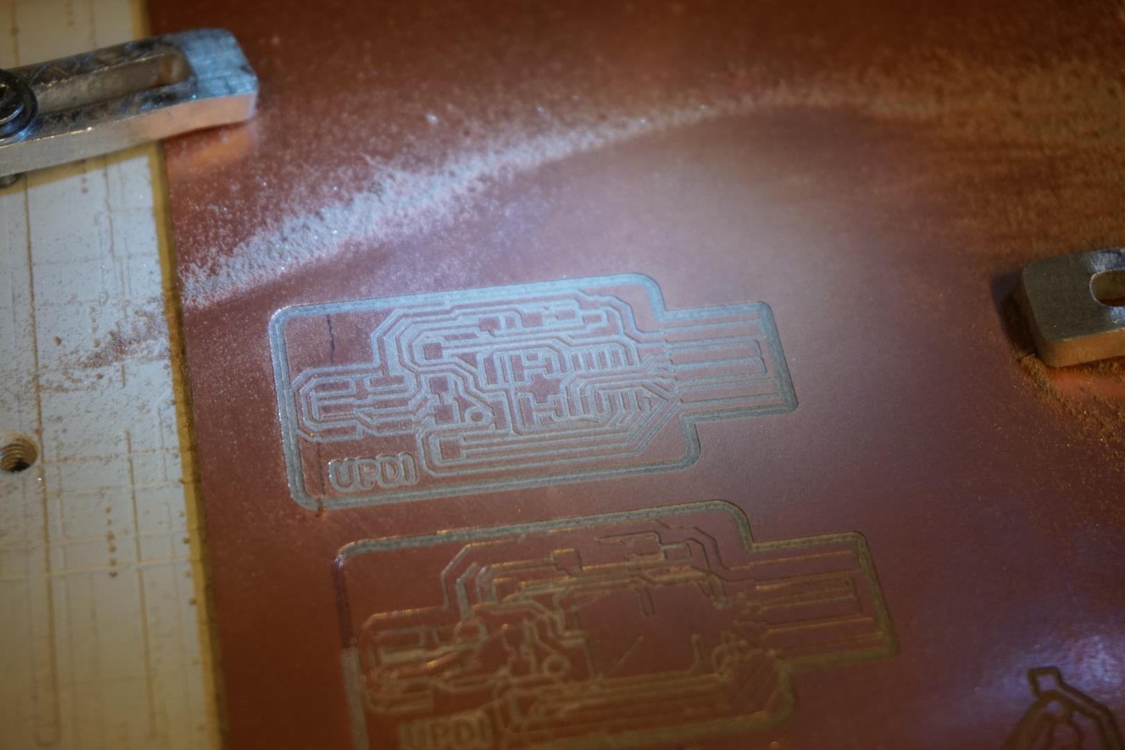
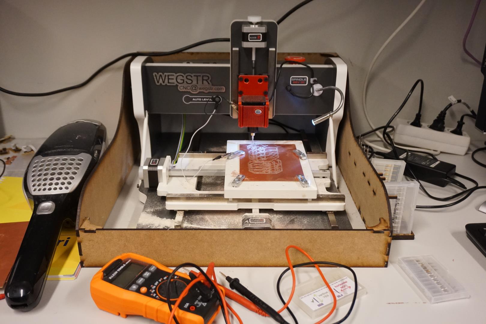
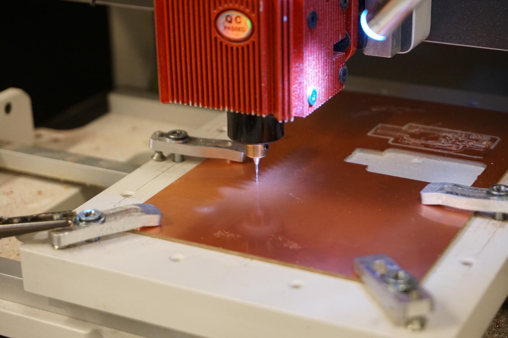
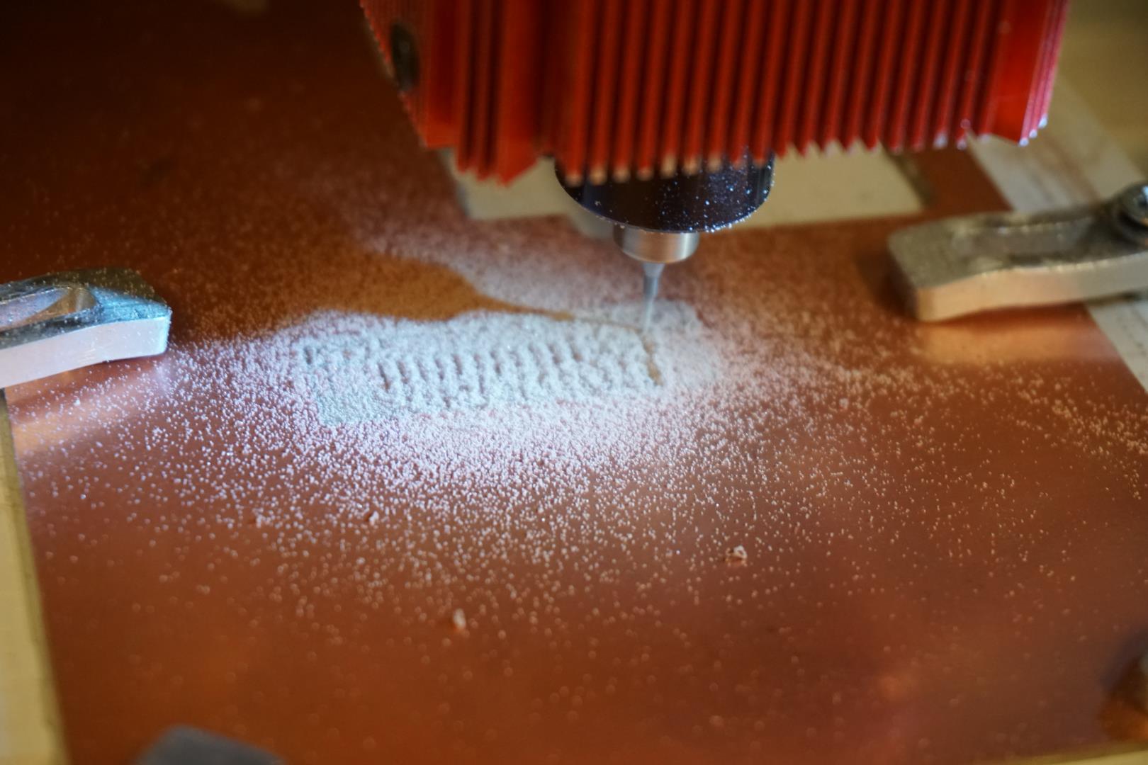
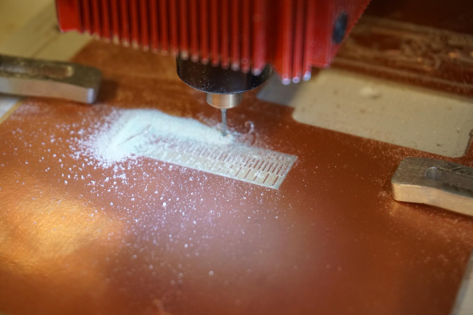
Cutting
I loaded the circuit trace file and started milling on the Wegstr.
We have two Wegstr in the FabLab, one new and one old. The new one was occupied by a student who was working on a project so I used the old one. The collet may be a bit worn down and the sacrificial board is a bit worn. I must not over-tighten the material, so it does not warp so I tightened it very lightly.
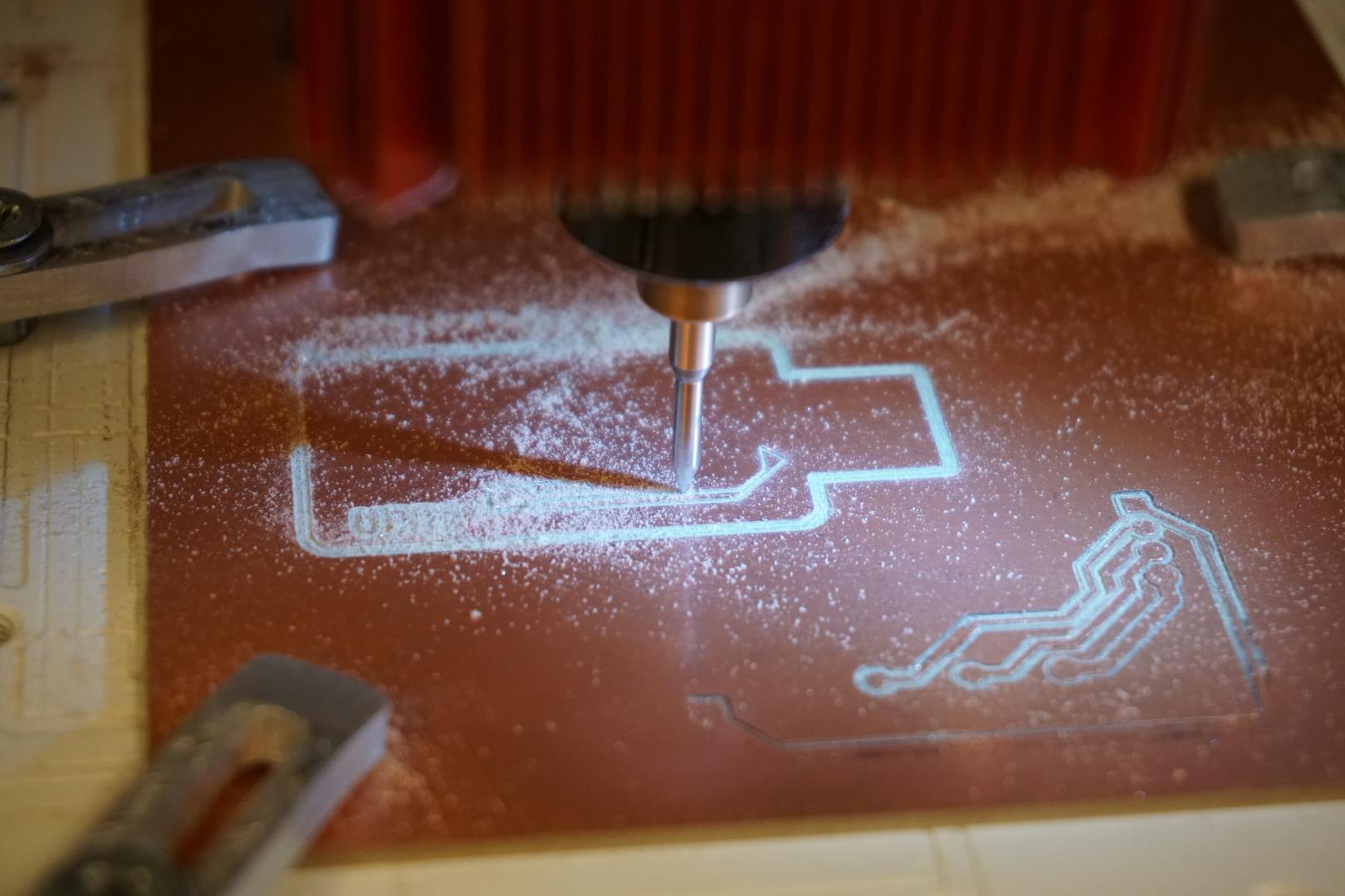
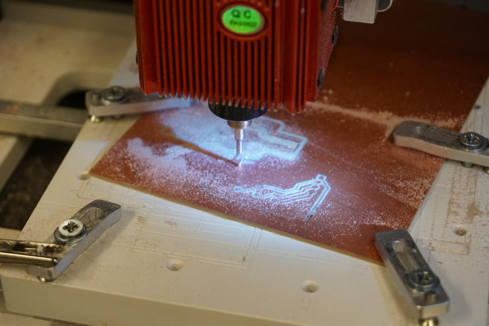
It was too loose!
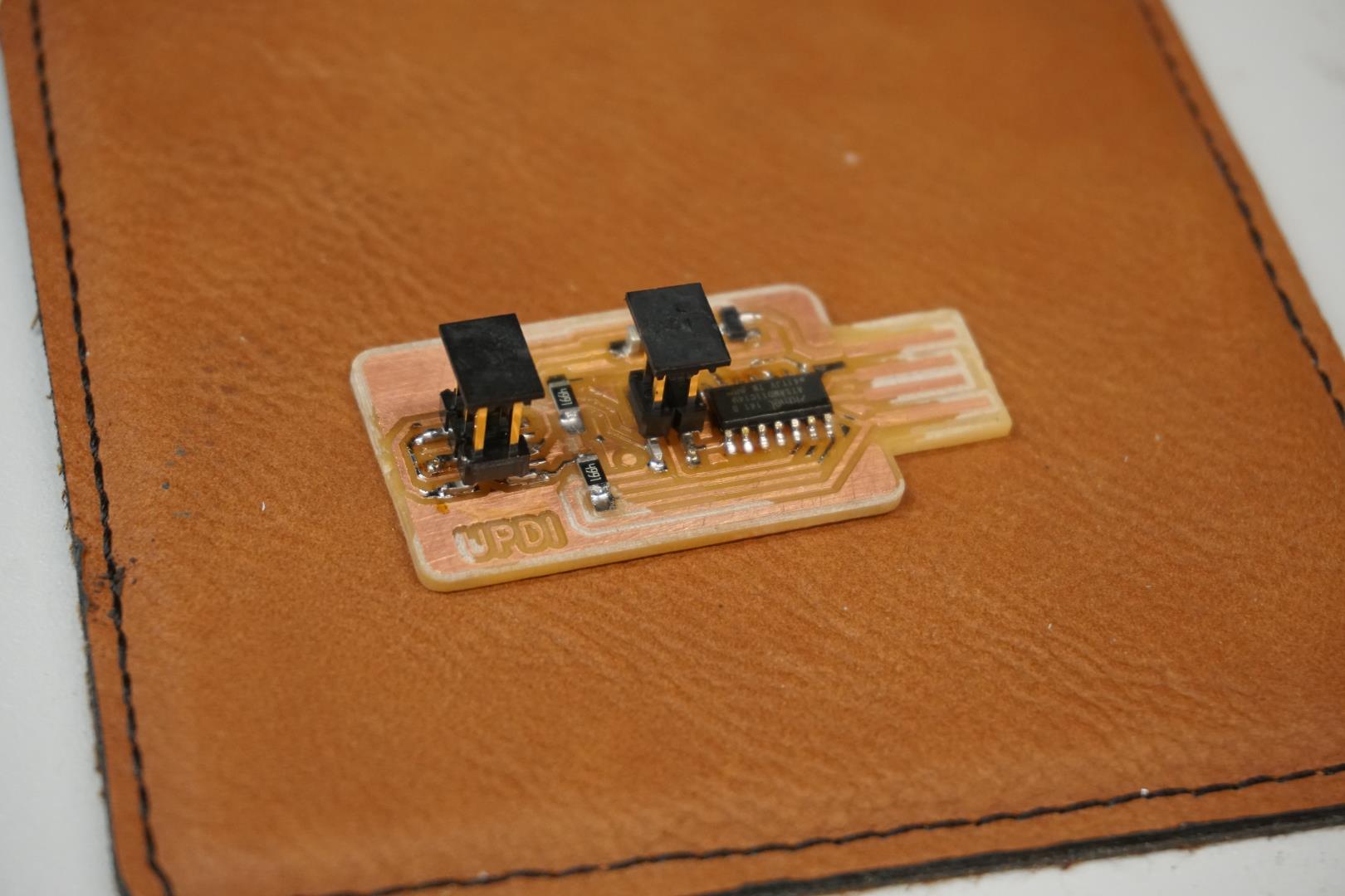
Soldering
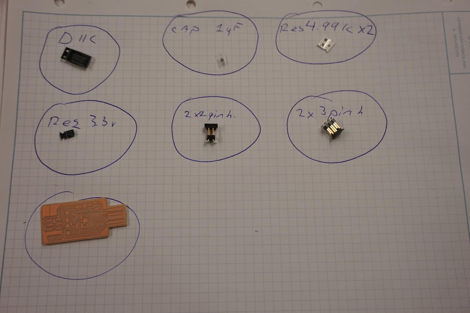
| Name | Component | Quantity |
|---|---|---|
| Microcontroller | ATSAMD11C14A | 1 |
| Resistor | 4.99k | 2 |
| Voltage regulator | LM3480-3.3V-100mA | 1 |
| Pinheader | 2x02_SWD_P2.54mm_Vertical_SMD | 1 |
| Pinheader | 2x03_P2.54mm_Vertical_SMD | 1 |
| USB | Conn_USB_A_Plain | 1 |
After cutting it out, I filed the edges and scratched the surface loosely to get better tin adhesion.
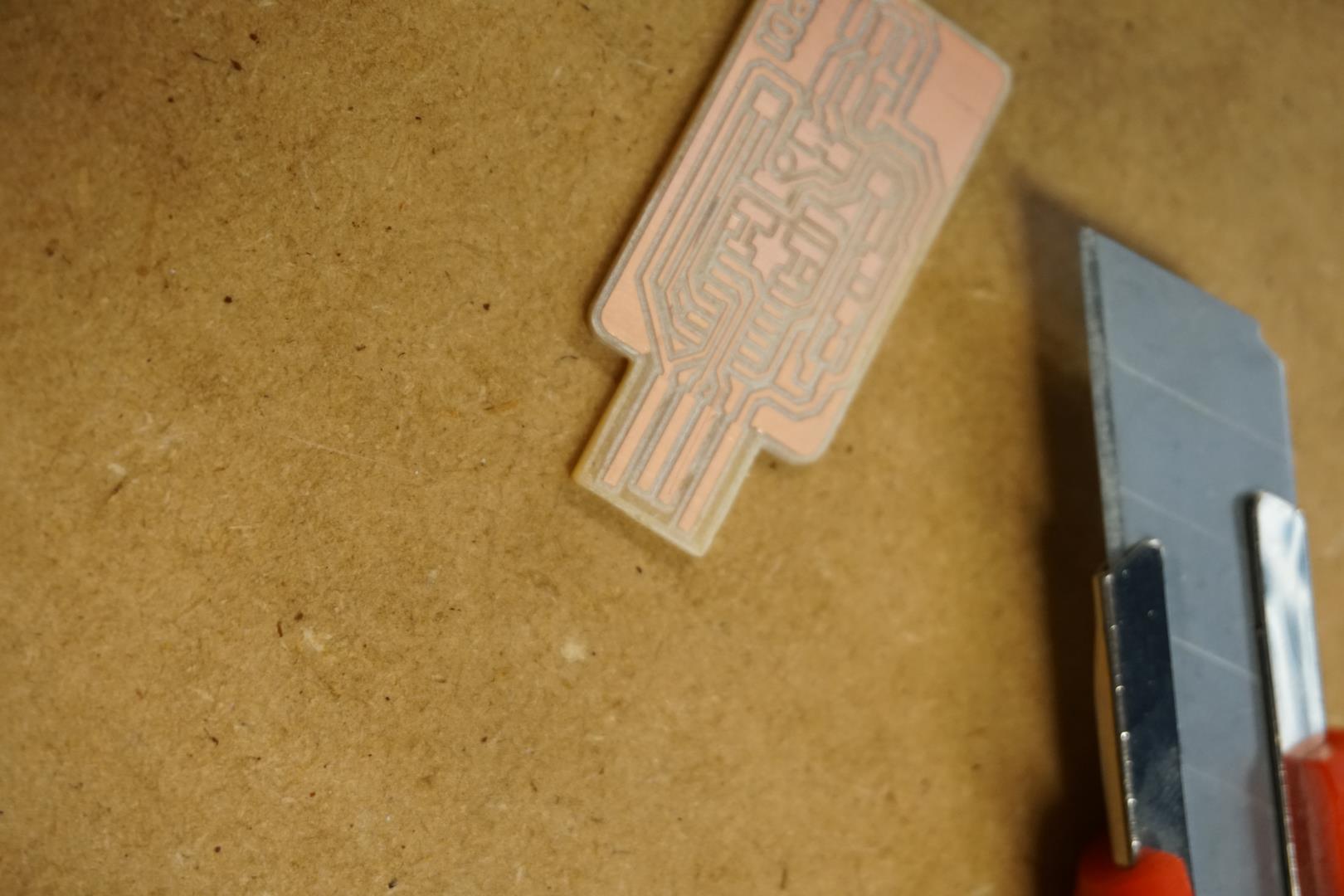
I then removed the extra copper from around the USB plug, just in case. It might cause a short circuit.
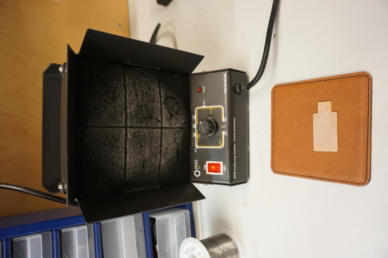
Setting up the soldering station. Leather pad to stop slipping and a fan extractor.
Following instructions for SMD soldering, I put a small amount of flux liquid on the copper and a small amount of solder on the surface. Then I placed the items, tacked it down and finished soldering.
The flux liquid works wonders and I had no problems soldering the components (or so I thought!).
Programming
Alright! Next up, programming the thing.
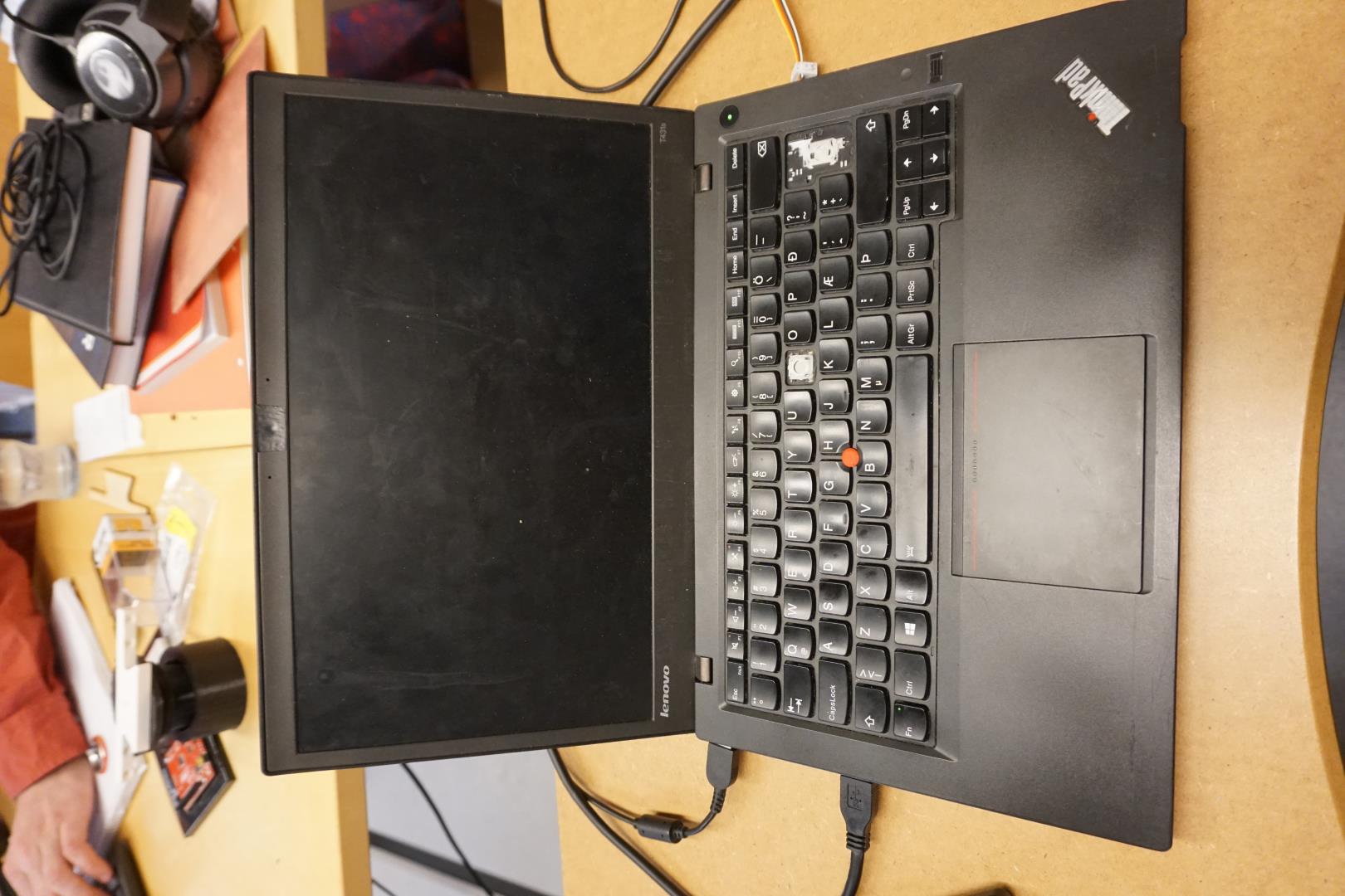
My instructor had already sent me a programmer, a SWD one.
I knew all these things work well in Linux, so I brought in my old laptop which runs 21.10.
I installed edb, got the firmware and ran the command:
edbg -ebpv -t samd11 -f sam_ba_SAMD11C14A.bin
but oh no! Turns out I had installed the GUI only version. Getting this url from my instructor, I got the CLI version.
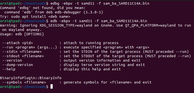
running again, with the CLI version I got:
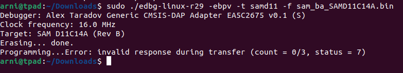
Hmm....
I discussed this with my instructor and together we studied the PCB, the repo from Kris I used, software setup and all that. We noticed a difference in the layout of the PCB, which turned out to be a update to the connector.
But after quite a bit of doing this and that, including:
- Designing the layout myself in KiCad (with the other one to copy)
- Updating the brilliant fab schematic library to the newest layout
- Installing and running the programming on my Windows computer, with the same error
- Almost overdosing on coffee
I turned the soldering iron on again, added plenty of flux and touched up all the connections.
Then I tried again, now with this command:
sudo ./edbg-linux-r29 -ebpv -t samd11 -f sam_ba_SAMD11C14A.bin
JIBBÍ!!
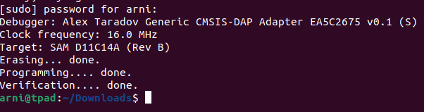
Now when I plug it in, it pops up identically to the one provided my instructor.
Great success!
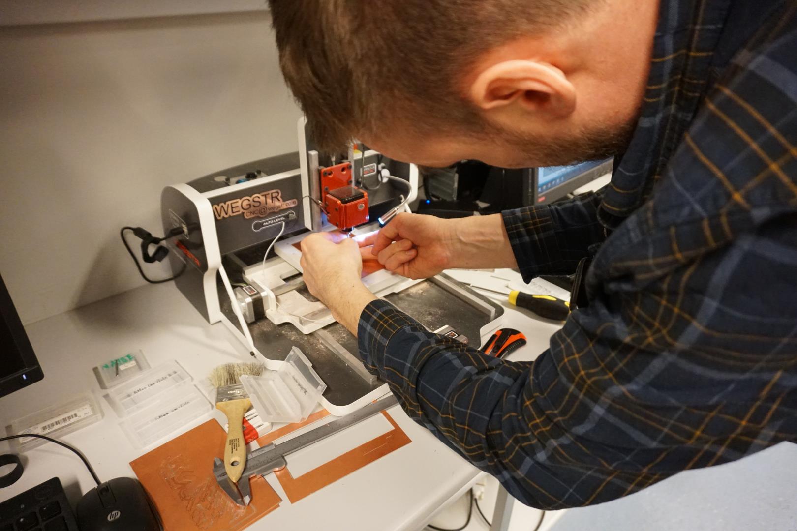
More milling!
Wegstr CNC mill
As mentioned before, we have two Wegstr CNC mill in the lab, in addition to our Roland mill. The Roland has been giving us some grief and dealing with that has to wait for a better time (or more money) and is out of scope for me during this week.
So, the Wegstr! I really wanted to try to do the line test from the Academy site, so here goes nothing!
Before further ado, let’s meet the Wegstr!
Wegstr interface
Here we have the Wegster interface. The screenshot below is taken during the line test milling documented below.
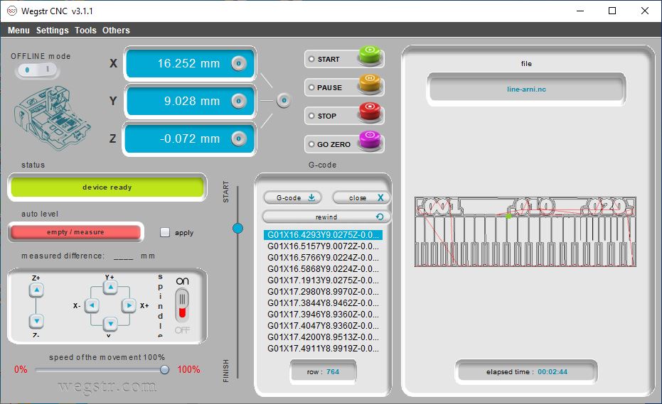
In the upper left/middle part, you have power controls and X,Y,Z values and reset buttons along with START, PAUSE, STOP, GO ZERO buttons.
On the right part, you get a preview of the milling path along with the mills current position (the little green dot).
On the lower left part you have device status (device ready / offline), auto level control, movement controls and a movement speed slider.
In the lower middle, you can load, close and rewind G-codes. To the left of it, you have the G-code progress bar.
Start milling
After mounting a PCB plate and the appropriate bit, you must:
- Open the Wegstr interface
- Move the mill to the correct position and reset x,y values (using the buttons)
- Either use the auto level function or manually set the zero point. (I seem to get fine results by using the manual method of lowering the bit to the top of the PCB and zeroing).
- Load the g-code file using the load button.
- Hit start, monitor the machine move to it’s starting point and confirm that the correct tool is mounted and the machine will start milling.
You should monitor it’s progress and use your ears to possibly adjust the speed. This is hard to describe in words, experiment and see what works best.
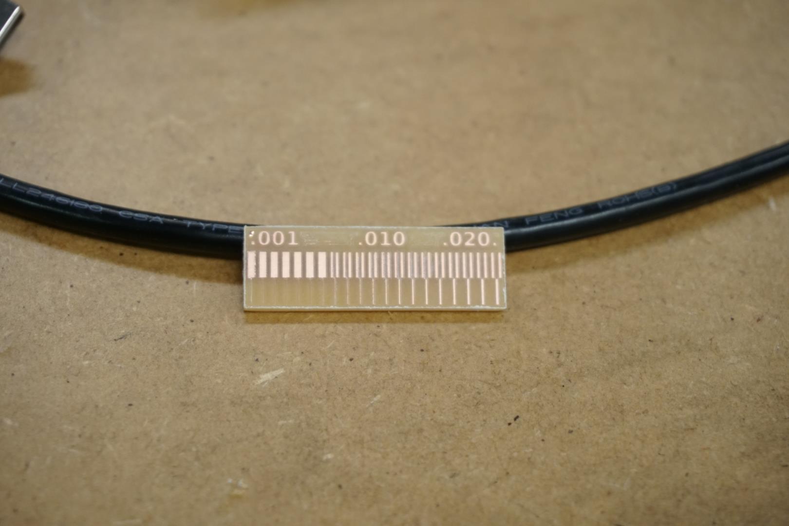
Line test - Weekend fail
During the weekend I tried to simultaneously entertain my three year old son in the FabLab and do the line test. Well, that was not very successful!

tl;dr: I had a bit of a failure using Fab Modules and had a bad drill bit.
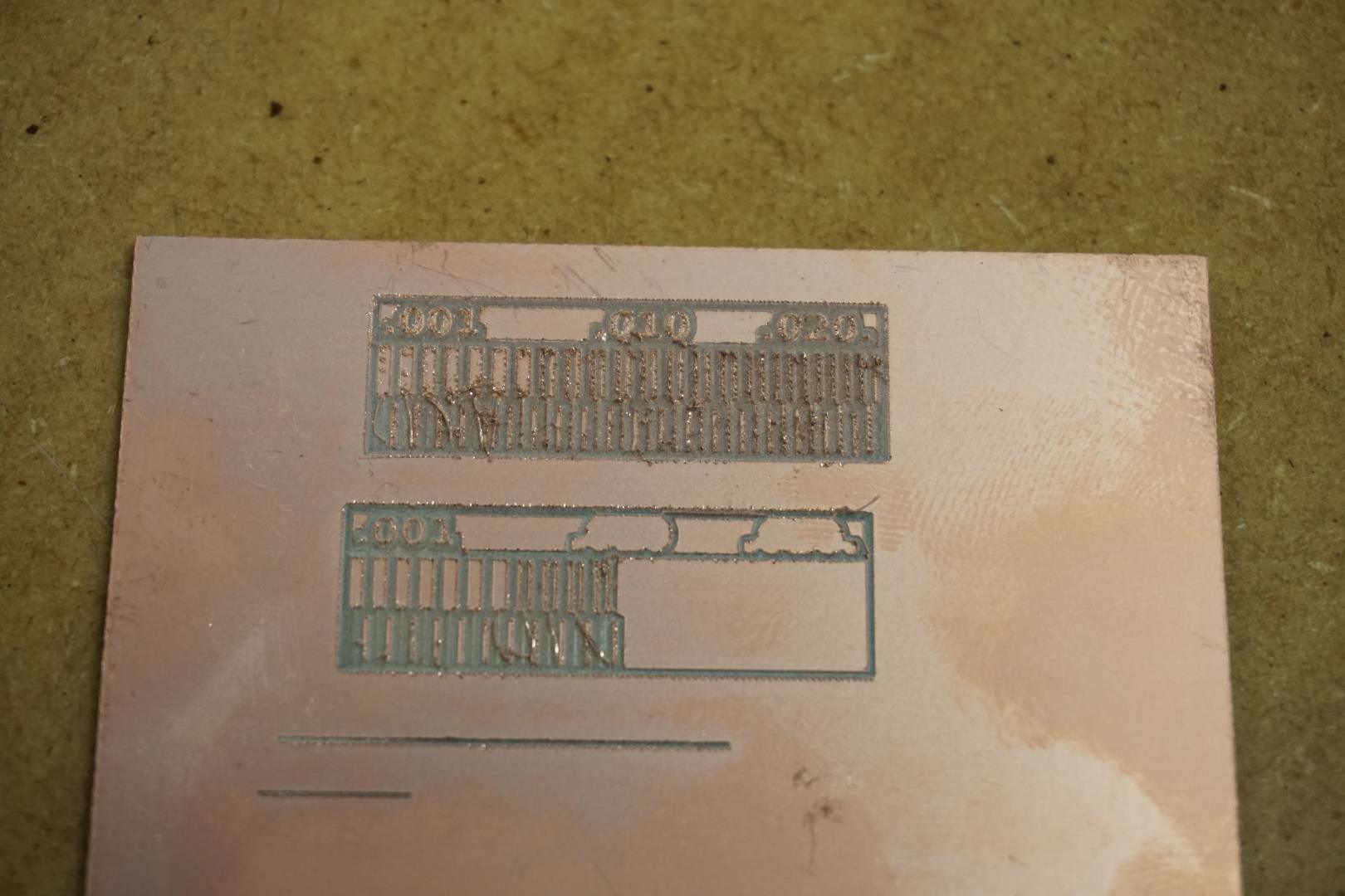
Line test - the good stuff (better at least)
So, after a few cups of coffee, a good chat with my colleague, I went for a second run.
This time I managed to do things a bit better. I used Fab Modules, specifically these steps:
Right click -> open server program -> mill 2D PCB png and got familiar with the options.
All in all, I made and used the following files:
| Line test files |
|---|
| 0.2 trace file |
| 0.4 trace file |
| 0.8 trace file |
| 0.8 outline |
The Wegstr has an autolevel function, but I did use the manual/gravity based method to zero the bit. I have my doubts about the function, though we might need more testing.
I used a flat 0.4 bit first, doing most of the milling. It did a good job!
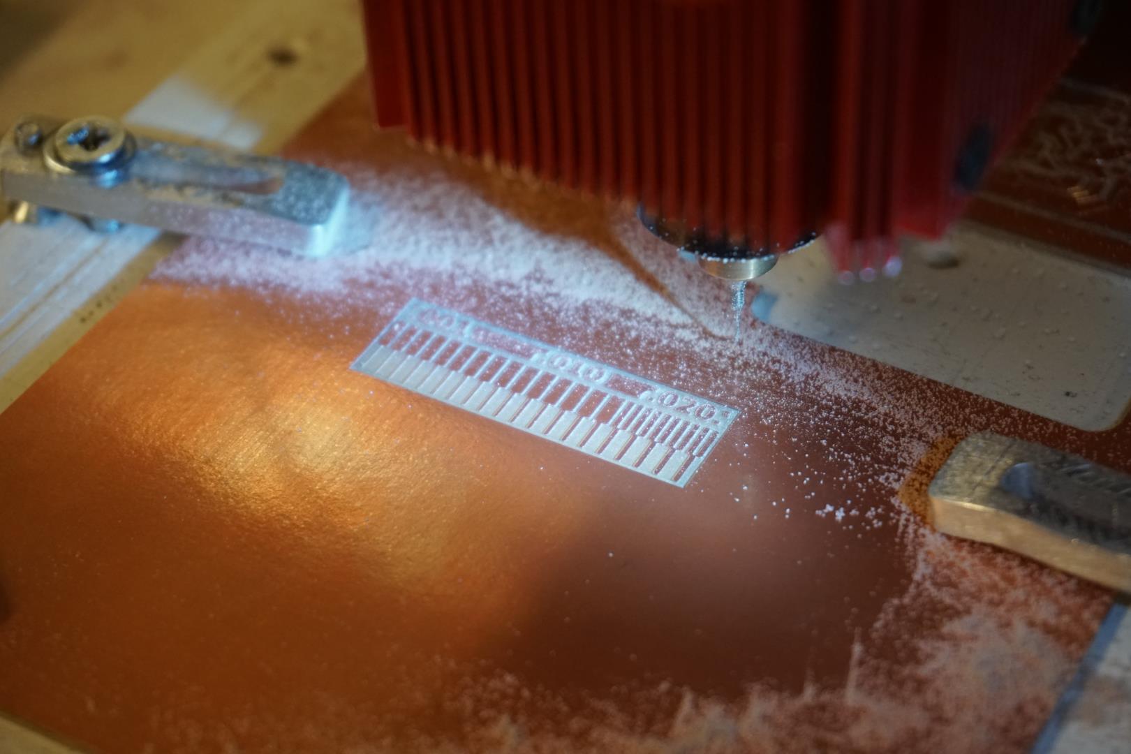
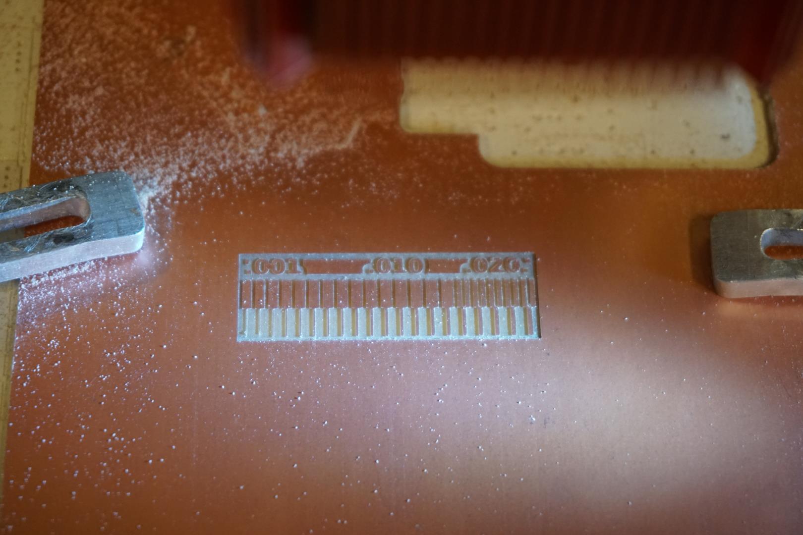
Next, I wanted to do the 0.2 mm tracing but we had trouble finding a 0.2 milling bit! What I attempted to do, was to use a V-bit. Now, what my sources tell me, is the V-bit actually has a tiny flat end, which should be roughly 0.2mm. But roughly is not perfect as we soon found out.
Any way, since this is experimental, I used the V-bit and tried it out. As I had adjusted the settings to 0.2mm, the toolpath now shows it would now attempt to make thinner lines, as in going further down the scale.
On the first run, we noticed that the bit was merely scratching/smudging the thin parts. To experiment, I simply edited the g-code file and replaced all the depth values of 0.07mm with 0.08. This did not change much.
Next thing I did was to replace the V-bit and found out that the one I had used was worn. This worked, it was much sharper but did strip away the thinnest lines. But it did make nice thin lines in the thicker parts (top part).
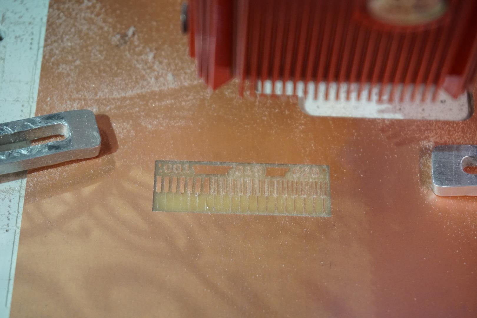
Then I loaded the cut out file and initiated the milling. It worked great!
Milling conclusion
I had my reservations regarding the Fab Mods, but once I got to know it, it started to make much more sense. I’m sure the different way each have their own advantages and disadvantages.
Board houses
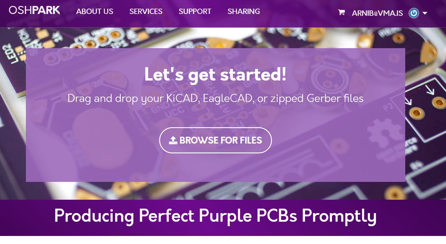
One of the intersted things mentioned during the lecture were board houses. These are companies that specialize in making PCBs, both for professionals and hobbyists. I’ve known of their existence for some time but never ordered from one. So I decided to try one out. I opened a bunch of the once mentioned on the Academy site.
I quickly found one I wanted to try out, with the purple color scheme and a p-p-p-p-punchy tagline:
Producing Perfect Purple PCBs Promptly!
Who could resist that?
Oshpark was the winner!
I created a user, fetched the above repo again and opened it in KiCAD.
The webpage simply asks for your design files, with a Browse for files button. It says acceptable files are KiCAD, EagleCAD or zipped gerber files.
Allright! Lets try it out! It says KiCAD, would it accept the project? First I tried upload the
.kicad_pro file but the site complained that I should use a supported filetype. Well, let’s try the .kicad_pcb file, that should make sense.
It started processing, but then gave the following error:
Sorry, we can't process files from Kicad development builds. Please submit gerbers instead. See help page.
Gerbers! I’ve seen Gerbers before. Here is a link to the Wikipedia page. So, lets go back to the KiCAD page and try the gerber files.
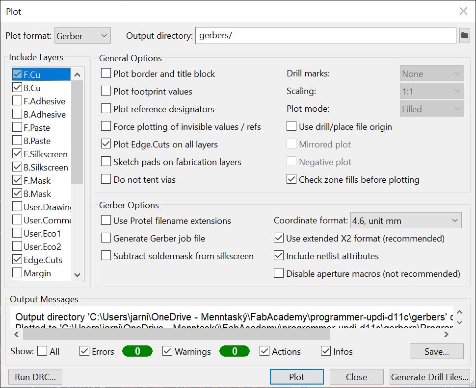
In KiCAD, you go to File -> Fabrication outputs -> Gerber files. Once you hit that, a dialog pops up and I just hit Plot and the files appeared in gerbers sub-directory.
The site asks you to zip them, so I did and uploaded them.
Success! I could see the design appear but there are a bunch of warning.
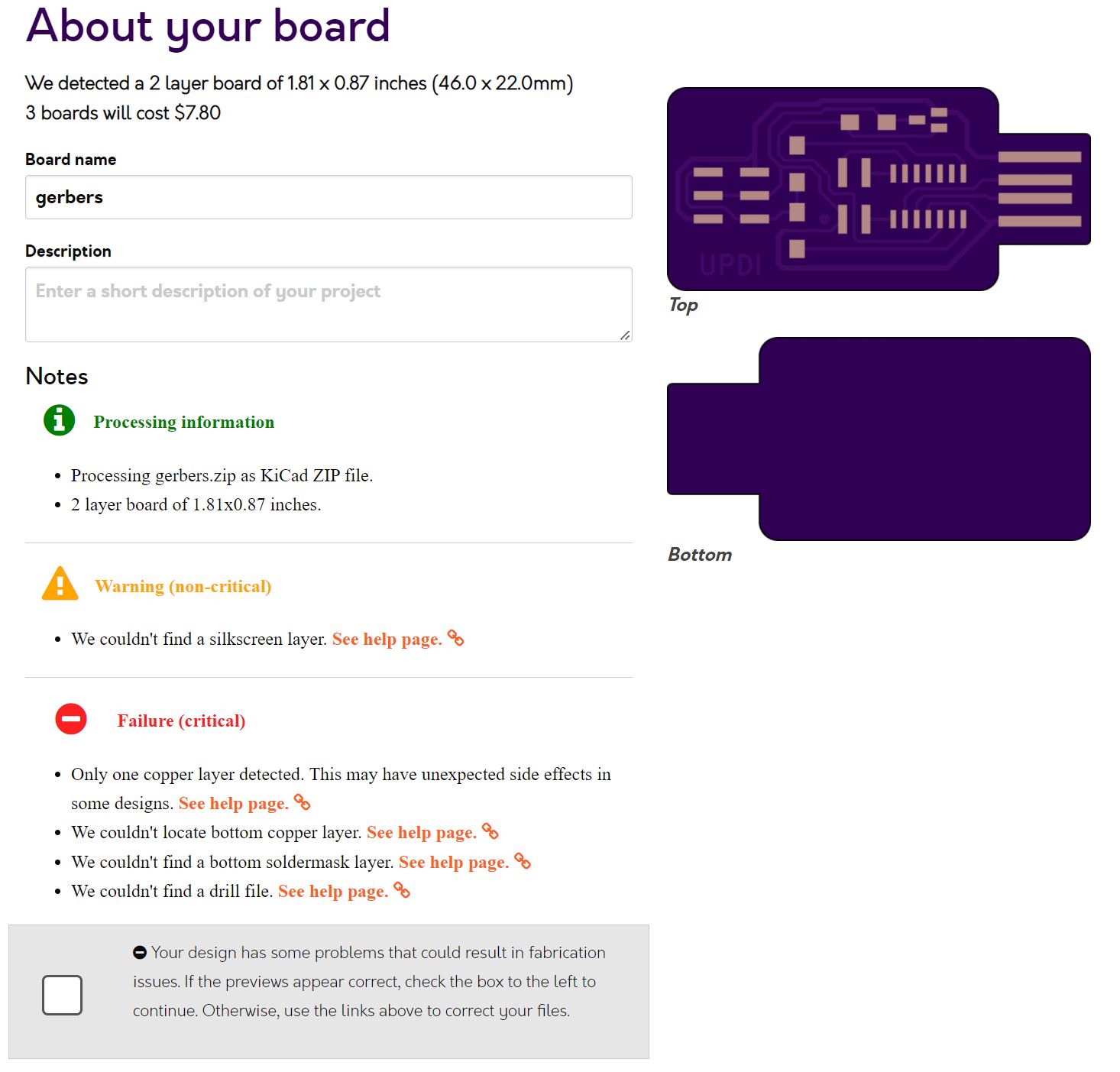
Hm, let’s dig into this a bit. It seems to have gotten the outlines just fine, as well as the components.
It reports the design to be a two layer board, although we know it only includes work on the one layer.
According to these warnings we need the following:
- Silkscreen layer
- Second/bottom copper layer
- Solder mask
- Drill file
Let’s try this again. Going the File -> Fabrication outputs -> Gerber files route again, but actually looking at the dialog helps.
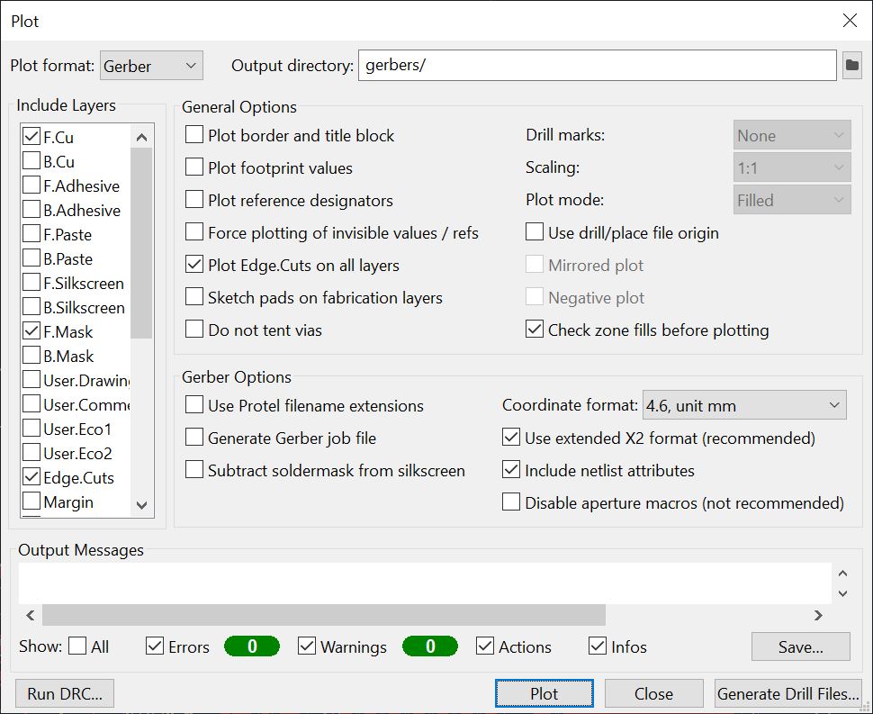
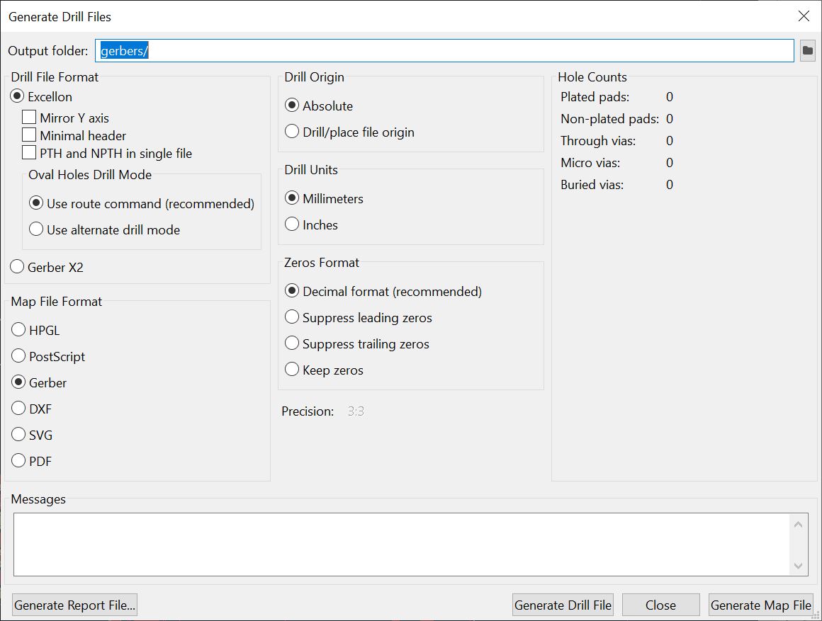
Turns out the default settings leave out the parts the boardhouse wants. So adding them, plotting again and also pushing the Generate drill files button return way more Gerber files.
So, zipping the files and uploading now reveals…
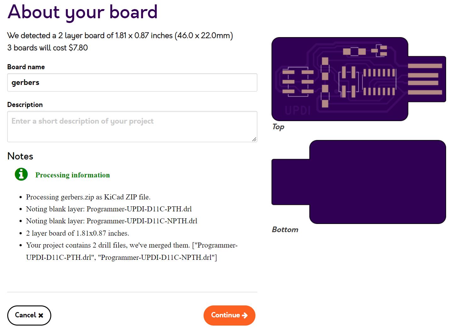
The system seems to be very happy with the files so let’s rename it and I also added the repo link to the description.
I hit continue and the site displays a summary of the project (too large to show here). I’m feeling adventurous, so I hit the Order button.
Next I can choose different options for my order, along with quantity. I chose After Dark option and 6 as a quantity. Three was the minimum but I chose 6, just for the fun of it. I’ll share the extra boards with those in need.
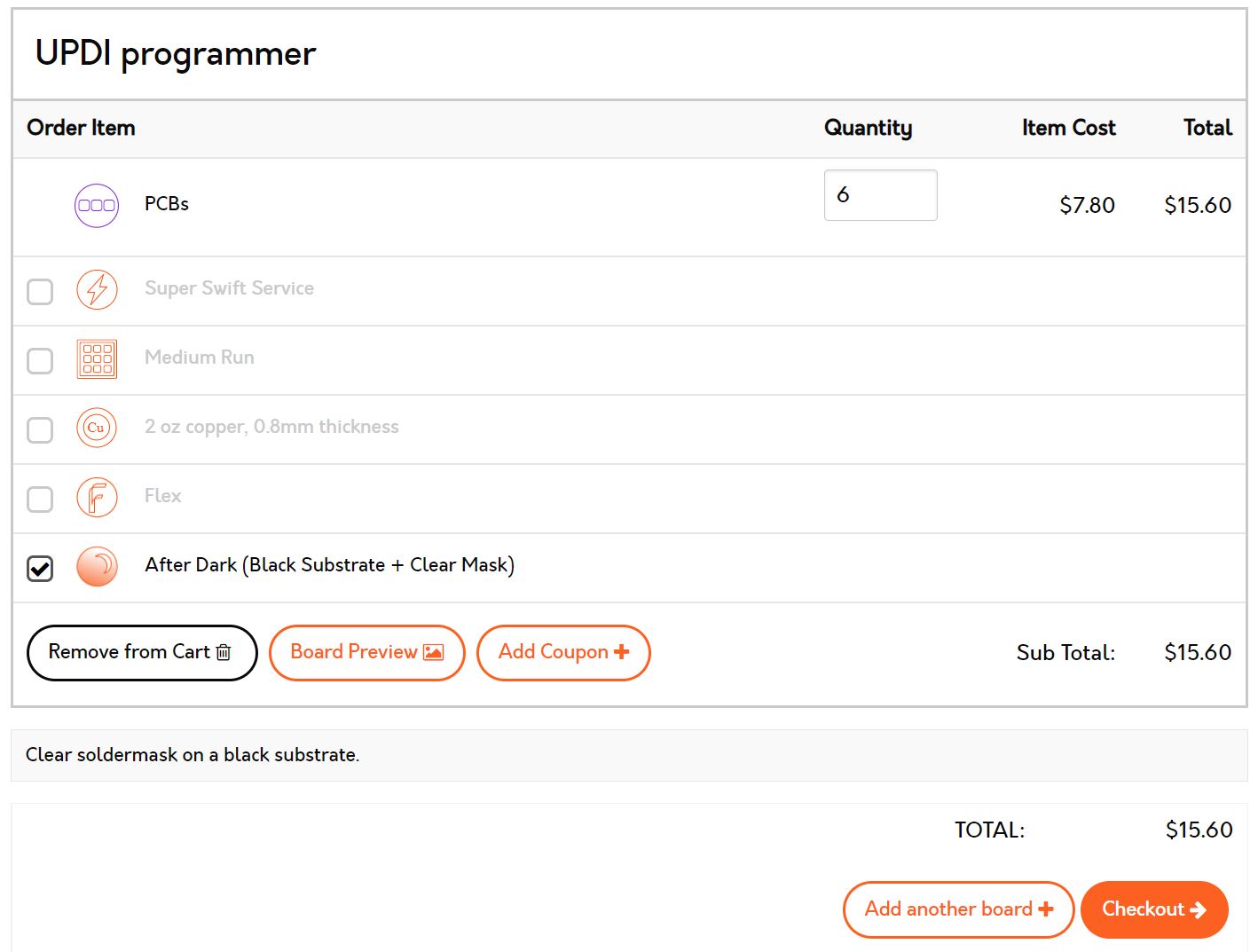
Im such a cheapo, that I chose the free shipping option. Total price: $15.60!
Lets see if customs will bankrupt me or not.
Delivery time is 5-21 days!
Below is the zipped file that I sent to OSHPark.
| Files from order |
|---|
| Gerbers |
Important update from week 04
My efforts to fix the problem with our labs sink has not gone unnoticed. In fact my solution is spreading. I caught a member of the faculty in our lab during the weekend, working with the vinyl cutter. This was the result:

Second important update from week 04
THIS JUST IN!: Another teacher dropped in, noticed the hot-fix and fell in love with it.