11. Output devices
welcome to this week’s assignment!, whew it has been a tough week. so this week we were tasked to work with output devices.
These are what we were tasked with: - individual assignment: - add an output device to a microcontroller board you’ve designednand program it to do something
- group assignment:
- measure the power consumption of an output device
Group assignment
The group assignment this week was to measure the power consumption of an output device this, so we measured the power consumption of a 12v dc fan. We did the task making use of an oscilloscope from aiisun(the EM125 model) and a multimeter from Kaiweets(HT118A model).*
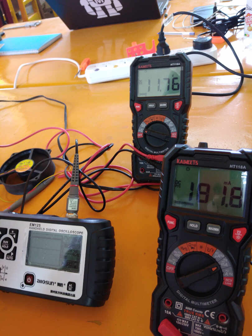 one oscilloscope and two multimeters were used
 measuring the voltage across the fan
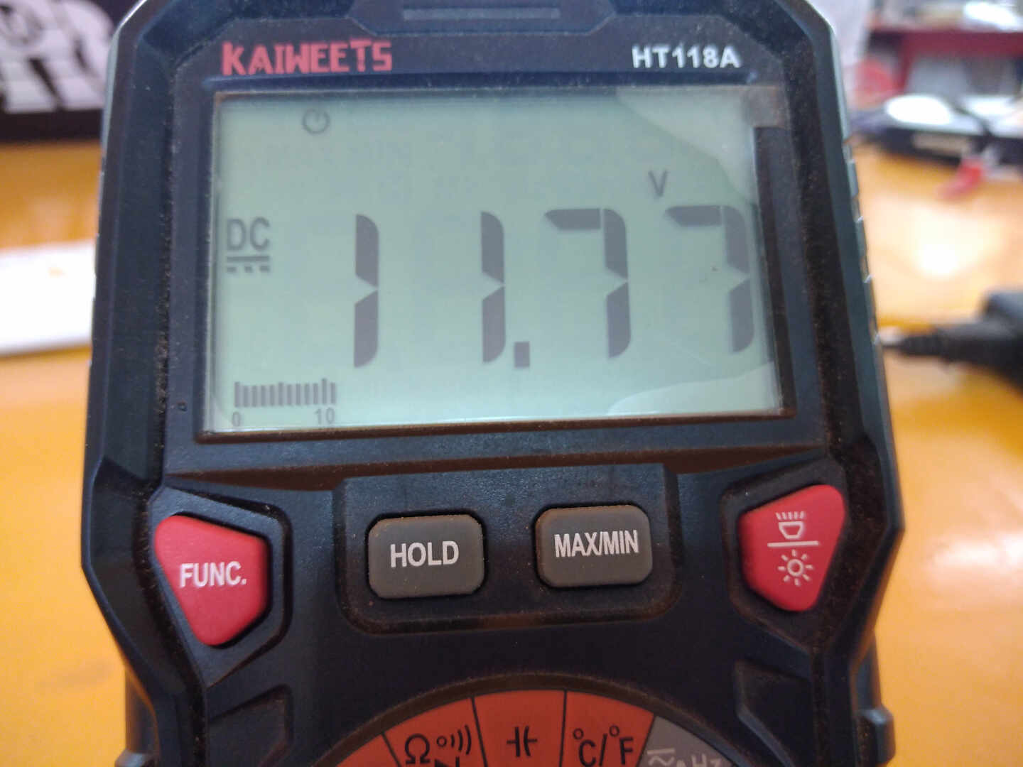 measured voltage read 11.77V
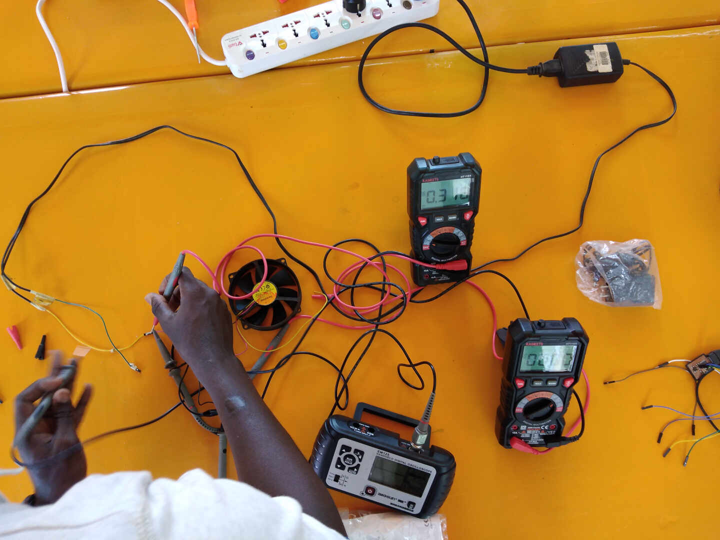 measuring the current run into the fan
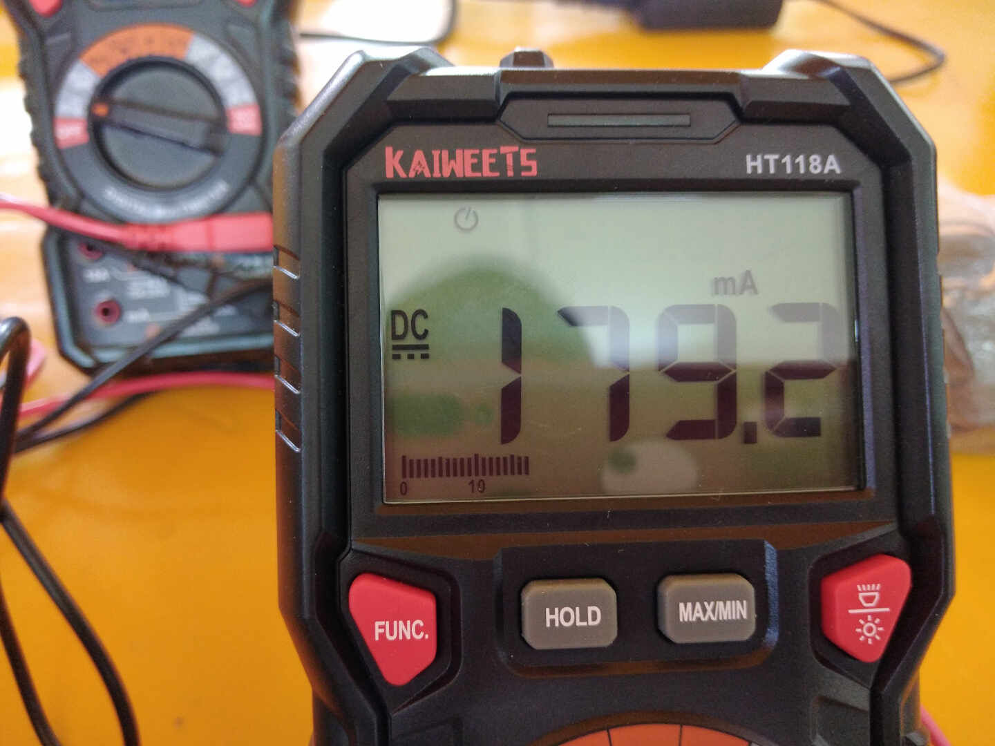 the measured current is at 179.3mA
hence the power consumed is = voltage * current power = 11.77V * 179.2mA power = 2096.64(VmA)
To read the current passing through the fan, the multimeter that was used for that was wired differently as compared to the multimeter used to read the voltage. The red cable was plugged into the red port labelled 10A as that port is used to read current that goes up to 10A and not blow the fuses in the multimeter.
Hero Shot
Individual Assingment
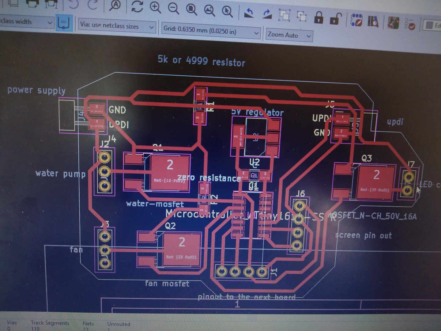
I had to design a new board for all my output devices since my PCB builds are geared towards my final project. My output board that is powered by an ATtiny 1614 chip will have the ventilation fan, water pump to irrigate the system, LEDs to lighten up the system and a 16x2 I2C LCD screen to display information to the user. So as usual, I used the KiCAd 6.0 Pro software to design the circuit board. but had alot of chalenges and errors as I progressed. I will share those chalenges and errors so you can avoid and find your way around them.
How it works
This is how the board is intended to work.
- An At-tiny 1614 chip willl beused to control the board
- A 12V to 5V linear voltage regulator will be used to step down 12 volts from the power source to 5volts to power the chip.
- The 12V coming from the power source will be used to power the fan, pump and LED strips since they are all rated at 12V.
- three mosfets will be used as logic gate for the fan, pump and LED strip since they are not powered by the chip. They basically acts as switches/gates for the chip to control the loads at the end of each mosfet.
- there are pull down resistors connected to all the mosfets
- There will be a capacitor for the chip
- there will be a two 4 pin out to connectors for the I2C communications and for out put to a screen.
the picture below shows an image that captures the PCB design of the first board I designed this week using the KiCAD 6.0 Pro.
the next Image shows the first board where I had finished soldering on the components and tried to feix the errors
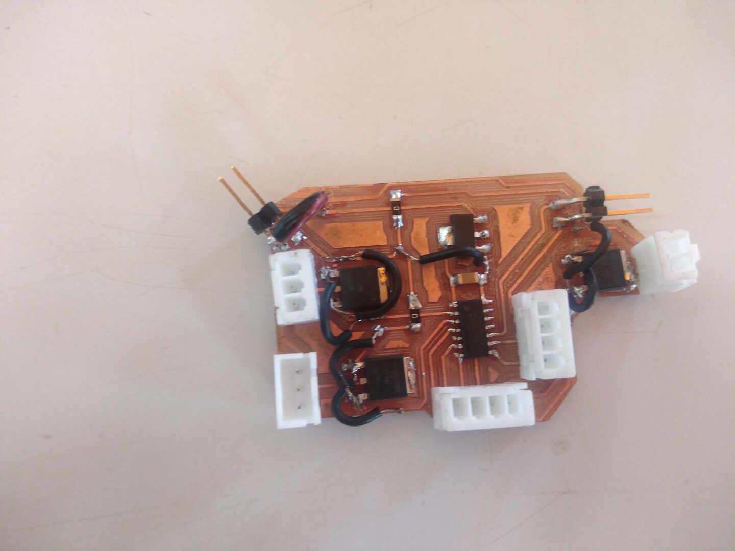 So these are the errors I made in the first board;
*I had switched the connections on the mosfets.I connected the source pin to the pin on the chip instead to the ground of the circuit and I connected the Gate to the Ground of the circuit. so I used the black wires you see in the picture above to correct and jump those connections
* The second error was i didn’t connect the ground of the chip, capacitor to the net ground and so I used a wire to try to fix that.
As you can see in the image above, the board looks nasty so I had to redesign to incoorperate the fixes to the errors
So these are the errors I made in the first board;
*I had switched the connections on the mosfets.I connected the source pin to the pin on the chip instead to the ground of the circuit and I connected the Gate to the Ground of the circuit. so I used the black wires you see in the picture above to correct and jump those connections
* The second error was i didn’t connect the ground of the chip, capacitor to the net ground and so I used a wire to try to fix that.
As you can see in the image above, the board looks nasty so I had to redesign to incoorperate the fixes to the errors
So I set about designing the new board
Below is the stage of the schemaitic design of the board
 in this I took my time to create a net ground and check all the connections to make sure I did not miss any.
The image below shows the circuit in the PCB editor window.
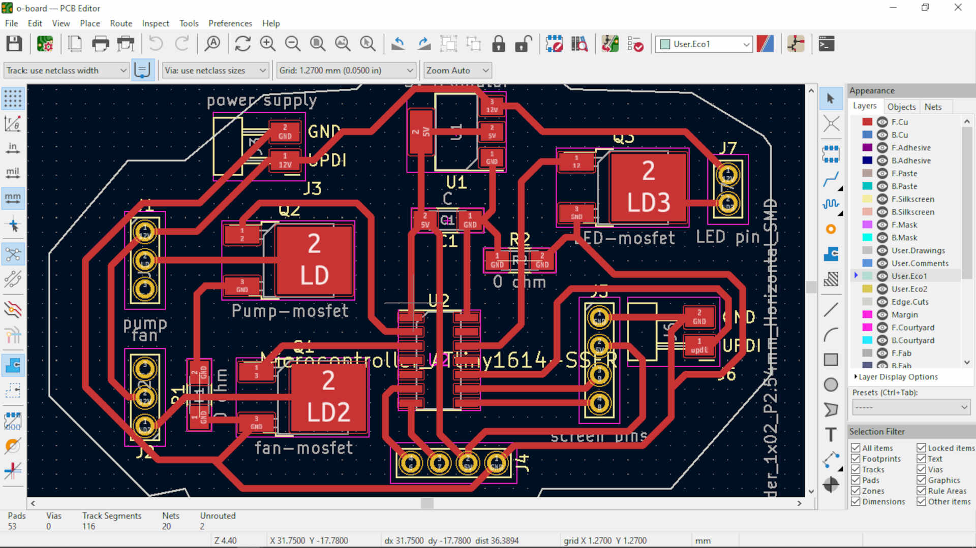 I laid the traces in this stage and defined the overall shape and edge cuts
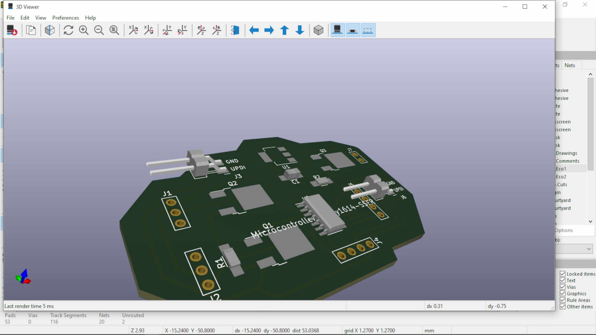
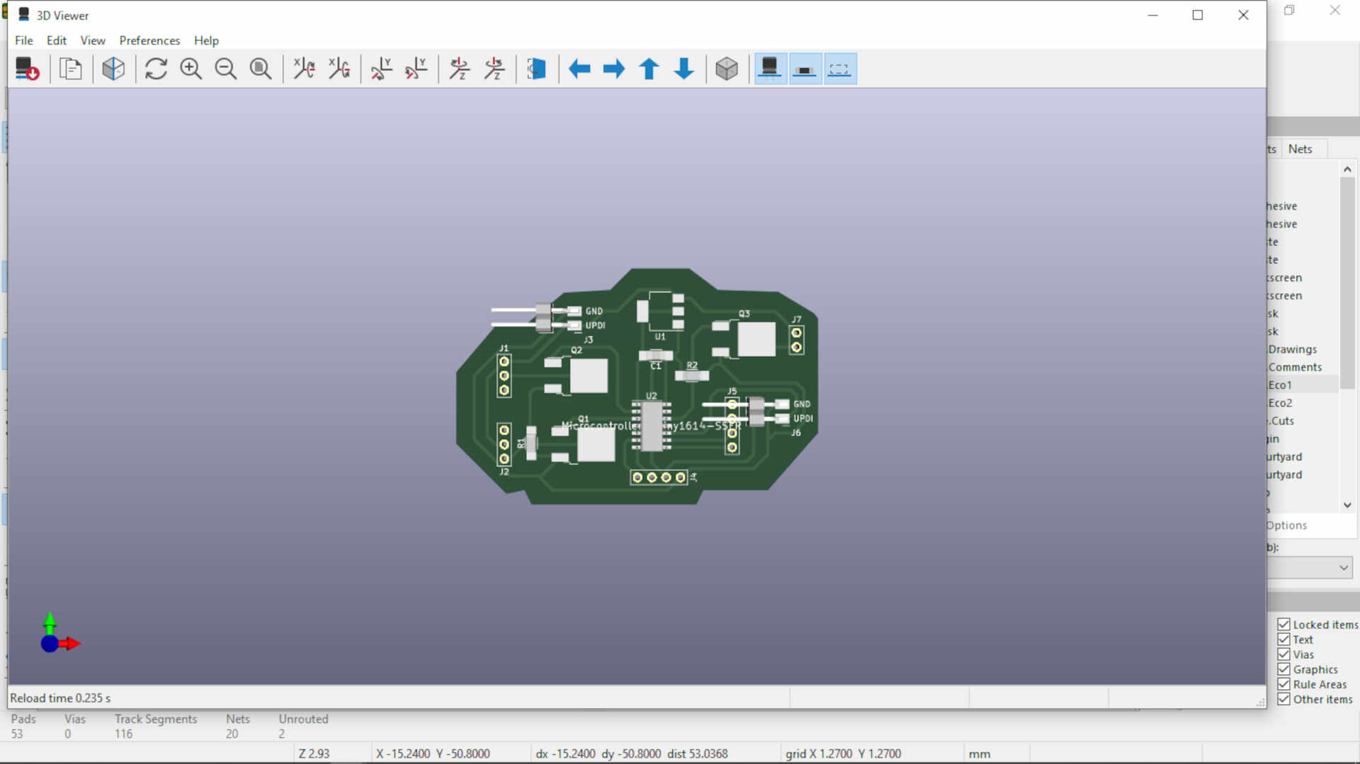
Images below shows the board with all its components in the 3D viewer window of the KiCAD software.
Now preparing the gerber files for printing with G-codes using Flatcam
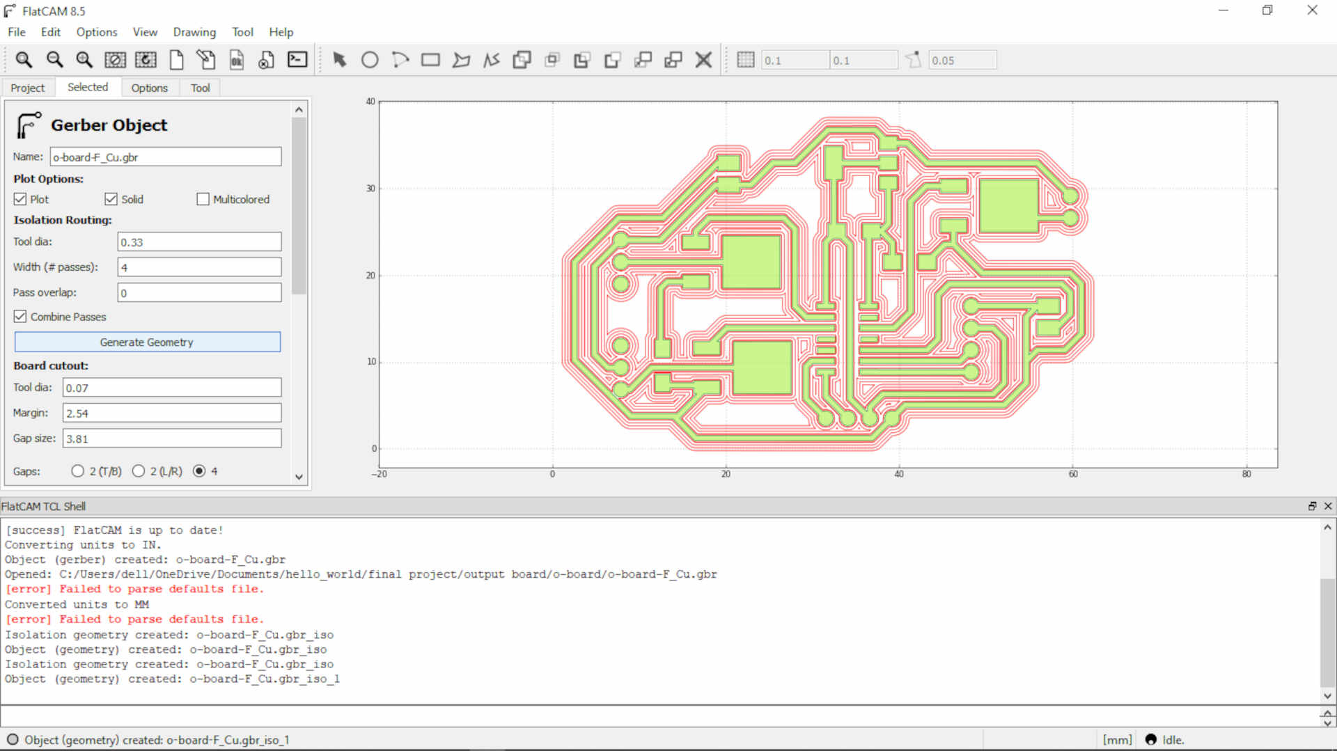 In the picture above, I set the tool diameter of 0.33mm and an overlap of 4 passes
 In the Image above, depth of cut was specified to be 0.08mm, feedrate of 60mm/m, Z positive travel of 4mm and a spindle speed of 10000rpm
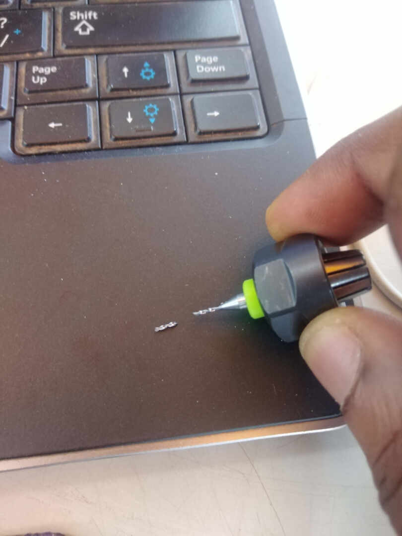
In the picture below shows a broken drill bit. this happened when I was leveling in the z-direction.the bit was close to the edge od the copper plate and slipped and broke.
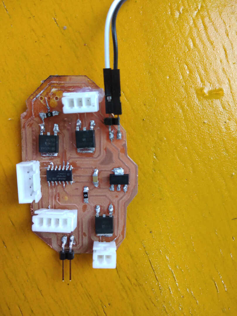
The Image below shows the machined PCB and components soldered onto the board.
Now we move on to the Test of the new board. I am testing the output of the fan for this Assignment. I will be programming with arduino. I wrote a simple programme to output through the fan.
Fan Test programme
int fan = 1;
void setup(){
  pinMode(fan, OUTPUT);
}
void loop(){
  digitalWrite(fan, HIGH);
  delay(10000);
  digitalWrite(fan, LOW);
  delay(10000);
}
This programme simply turns the fan on for 10 seconds and turns it off for 10 seconds.
Changes made
I made some changes to my board design as I progress through out the weeks of developing my final project The images below shows the Changes made to the designs:
- I added an FTDI connection port
- Changed the shape of the board and the arrangement of the components
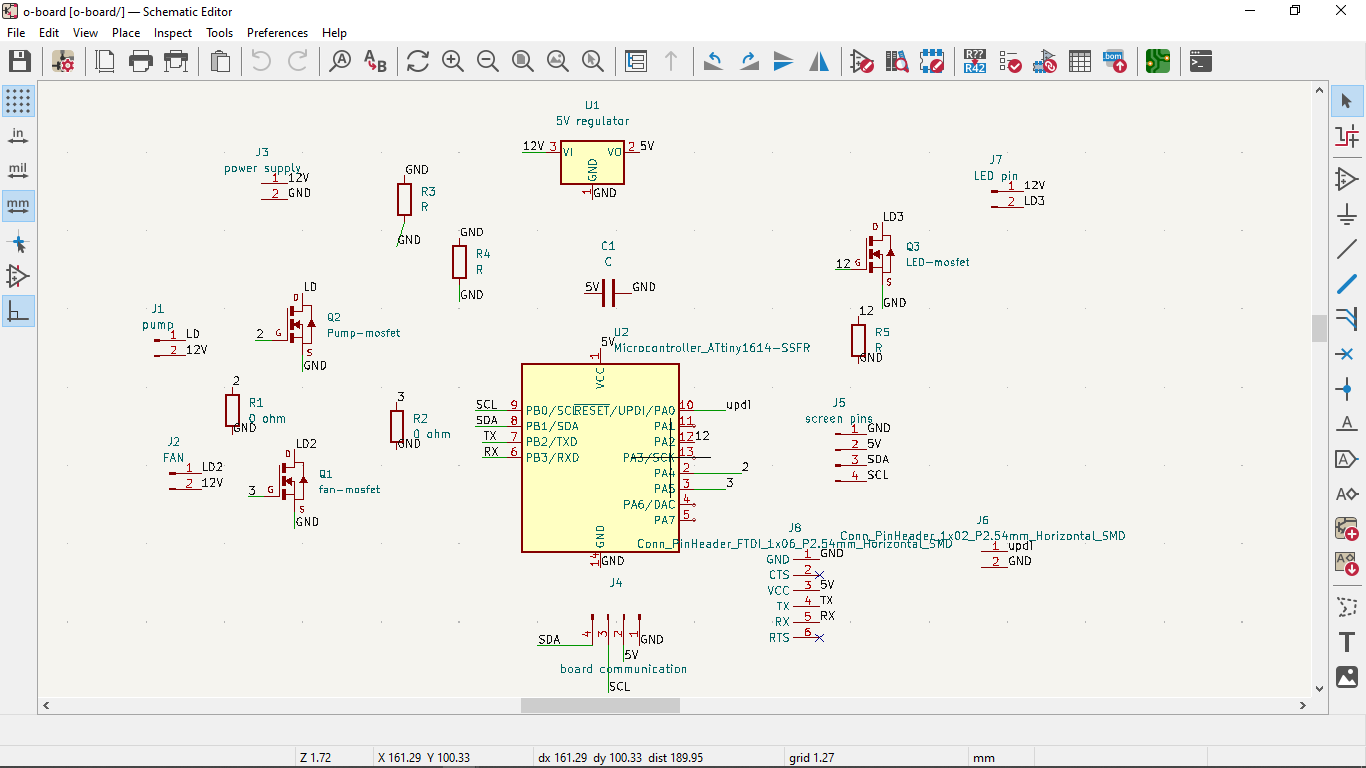 image: schematics
 image: PCB design
files
Output_copper_traces Output_edge_cut Output_drill_holes
What Went Wrong?
Broken bits and loss of some copper traces
what went well
the programming and group assigment went on smoothly
Wrapping Up
it was a fun week, the basics for my final project output board was developed in the week.