5. Electronics production
This week I worked on production of PCB for electronic systems. That is cutting out the traces and board with a CNC machine and then soldering the components onto the cut board.
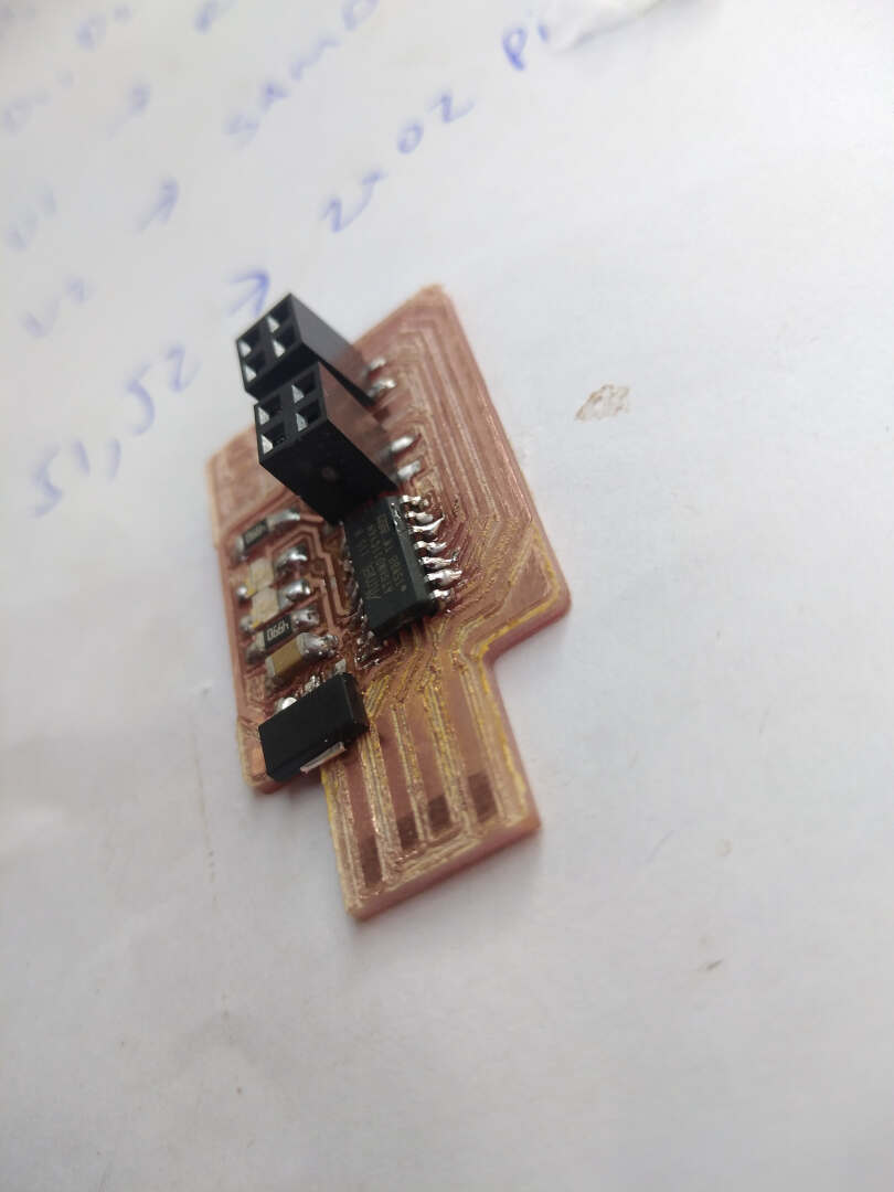
Hero Shot
Here are are some hero shots of my finished board. (Ps. the camera quality is bad)

Group assignment:
Characterize the design rules for your in-house PCB production process: document feeds, speeds, plunge rate, depth of cut (traces and outline) and tooling. document your work (in a group or individually). Document your work to the group work page and reflect on your individual page what you learned.
Individual assignment:
Make an in-circuit programmer that includes a microcontroller by milling and stuffing the PCB, test it to verify that it works.
Group Assignment
The objective of the group assignment was to Characterize the design rules for our PCB production process: document feeds, speeds, plunge rate, depth of cut (traces and outline) and tooling, and document our work (in a group or individually). To begin, I will start with describing the hardware.
 Above is the CNC Machine used.
The CNC hardware technical specifications are as follows: CNC 1610 PRO Milling Machine 3 Axis GRBL Control DIY Mini CNC Router Kit Engrave PVC,PCB,Plastic,Wood Router Engraver Engraving Machine CNC1610 Pro with ER11 Collet (1610 Pro) here
the first part of the group assignment was to learn how to use the machine, this included loading the cutting piece, working with the software, changing the bit, and starting a carve.
For our first test, we used the Flatcam with different parameter and recoreded the observations made.
 imag: Flatcam 8.5
The bit used for these tests has a size of 0.1 mm. we observed three settings concerning the depth of cut, the first at -0.05mm the second at -0.07mm and the third at -0.1
 image: copper plate secured and bit loaded.
The tests were started by zeroing the z-axis using our eyes as measuring tool, but realized we had low accuracy for our depth of cut. Then our instructor showed us a simple zeroing techinque using a piece of paper. The paper was placed on the copper place which is securely placed on the bed, the paper was moved back and forth on the flat surface of the copper plate whiles lowering the z-axis until it touches the piece of paper which will kind of restrict the paper’s movement. Then we remove the paper and then move the z-axis 0.01mm 8 times to touch the copper plate.
 image: showing various depth and zeroing techniques used.
 image: Paper zeroing technique
 images: bits
some calculations were made to find the depth of cut.
 .
.
Milling
We used Mods to generate the .nc file needed for the milling machine. Then we used Grblcontrole-candle for the communication. Here are the procedures to generate the file and send the file to the machine.
Opening Mods
The mod interface and parameters set.

The Grblcontrole-candle and milling process

The finished mill of the test traces

Individual Assignment
when we were done with the group assignment, I begun working on my individual assignment with the recording of the right parameters of the cnc machine. I used Flatcam 8.5 to set the parameters of trace milling and board cutout.
Job Specifications
For milling the traces of the board these were the best parameters used
tool diameter: 0.38mm
tool depth: 0.08mm
feed rate: 90mm/m
spindle speed: 10000rpm
travel z: 1mm
cut z: 0.08mm
For milling out the board cut these were the best parameters used:
tool diameter: 1mm
travel z: 1mm
cut z: -1.5mm
feedrate: 60mm/m
spindle rate: 1000rpm
Milling
Files for the traces

 image: Traces of the PCB in flatcam
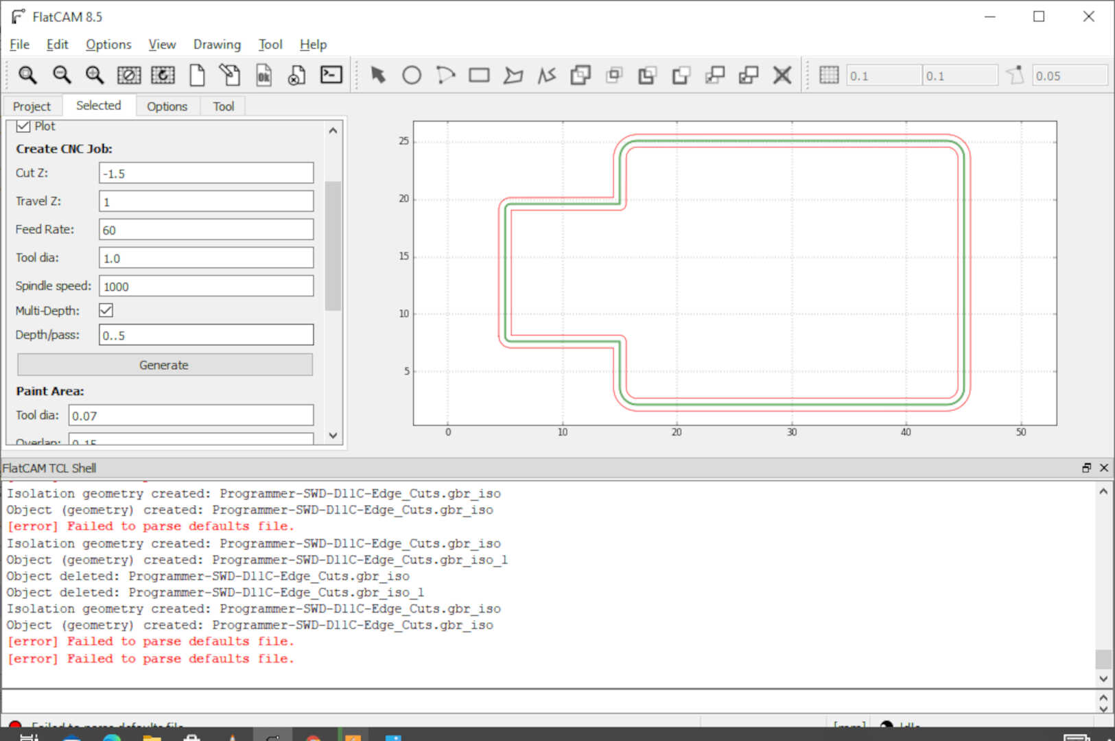 image: Cutout of the board
 image: miling the traces
 image: cleaning the PCB with alchol
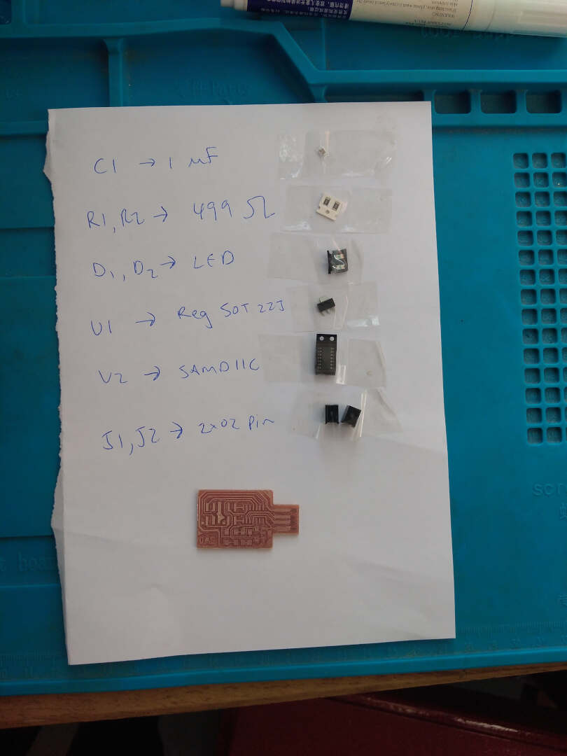 image: with list of components to solder
Soldering
 image: me soldering the components onto the Board
The Samsout 858D hotair soldering station and the klaryma soldering kit will be used for all my soldering task for this and the rest of the assignments for Fabacademy 2022. The hotair station was operating at 285 degress celcius. I used it to solder the microchip onto the board, the soldering iron from the Klaryma kit was used to solder any other component to the board and waws operating at 300 degrees celcius. Fortunately for everything went on smoothly.
 the Samsour 858D station
 the KlaryMa kit
image: finished board with components
 image: testing it by plugging into a usb port on a computer
Flashing the DAP programmer using Raspberry Pi
1. Start by configuring your Pi
To begin, we used the “The following link” to learn how to use Raspberry Pi as a porgrammer through open OCD.
1.1 Install open OCD dependencies.
On windows you will have to first install “libusb” and donwload the latest Windows binaries.
Next, clone the OpenOCD repository onto your computer using the following command.
git clone --recursive git://git.code.sf.net/p/openocd/code openocd-code
cd openocd-code
I faced a problem cloning the openocd repository, but got help. The problem was that the raspberry pi did not trust/ use the openocd site certificates.
I did a little searching on the internet and came across a website giving solutions to the problem step by step.
I did a further search on electronic production using the SAMD11C14A chip and came across Quentin’s blog. His blog perfectly records into details how to programme the SAMD11C14A chip, but unfortunately for me I ran into dead ends with three SAMD chips and 2 re-milled PCBs. One of the chips was burnt due to a malfunction of a voltage regulator I used. The next one didnot work so I replaced it with a new chip and to no avail that chip had the same errors. I will show the errors I faced down below.
I tried programming it using an Atmel ICE programmer and a Raspberry PI 3 but none of these processes where sucessful.
 this image shows the board connected to the Atmel ICE programmer using jumper wires and the smd header configuration found here but to no avail.
I used the [openocd] method and the [EDBG] method found in Quentin’s blog
this image shows the board connected to the Atmel ICE programmer using jumper wires and the smd header configuration found here but to no avail.
I used the [openocd] method and the [EDBG] method found in Quentin’s blog
 In the image above, you can see the errors when I used the openocd it states: Error connecting DP: cannot read IDR. I googled this error and the suggestions to solutions were hardware problems so I re-milled a new board changed the Chip and the connectors but still faced that same problem. At the end of the image, you can see I tried the EDBG method too and got an error : unable to open device /dev/hidraw2: permission denied. I looked up this error to and the solutions I found required me to edit some files in the raspberry system files which is way out of my knowledge league.
 The image above shows me connecting the board directly to the Raspberry Pi 3 using jumper wires. These connections were made using connection image in Quentin’s notes. Unfortunately this didn’t work too. the errors I faced are below.

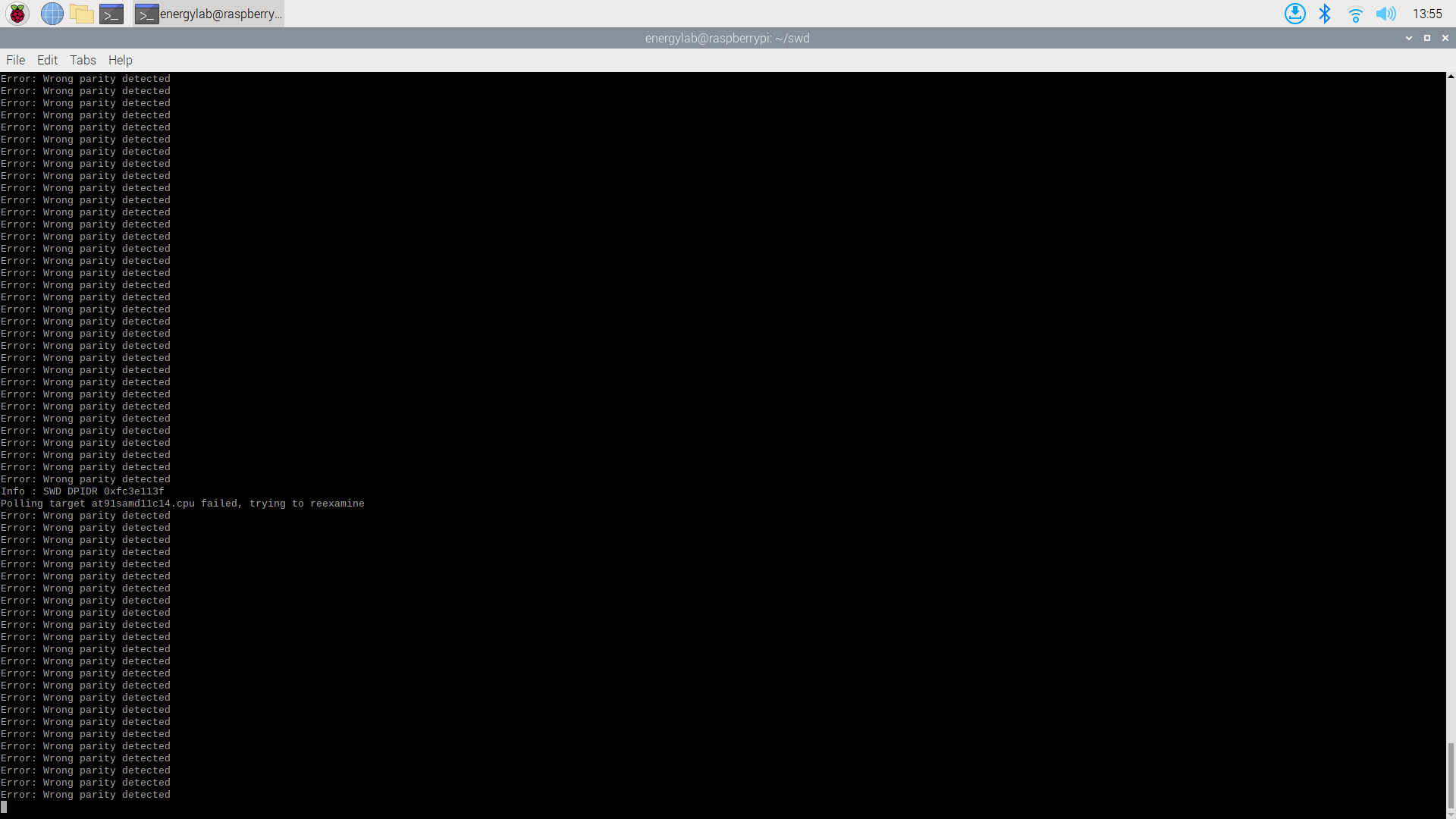

In the images above shows the errors I got when I tried the openocd with the Raspberry pi 3. so with consultation with our instructor, I was advised to switch to a updi programmer using FT 23X series chip. the next section will detail that process.
FT 23X series build
I tried to reused an old FT230 chip but a pin broke off from the chip and the unfortunate thing was it was the only FT230 chip our lab had. unluckly we had an old uart programmer laying around so I decided to reuse the FT 232Rl chip on that board.
 the image above shows it(image quality of my phone got bad as I zoomed in).
So de-soldered the chip from the board and got to work redesigning a PCB to match my needs
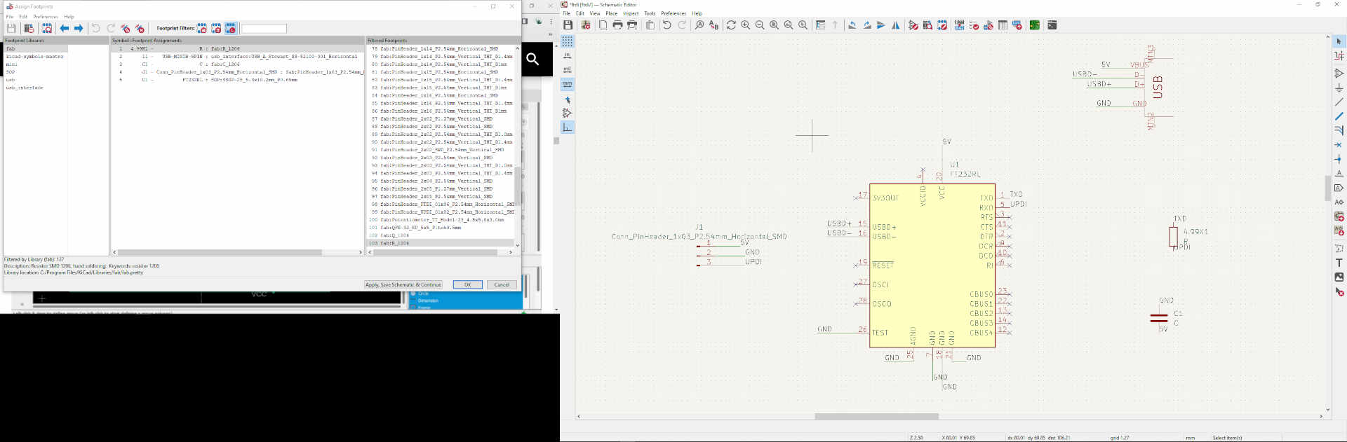
 the two pictures above shows the schematic and trace layout of the new board for the updi programmer


these three pictures above shows me generating the Gcodes of the traces,edge-cuts and dill holes of the board using flatcam


these two images above shows the board being milled and when the milling process is complete

this image above shows the board when all the components are soldered on to it
I connected it to my computer and used a multimeter to read the voltage going to the pin since I didn’t add an led to the design and all checked out good.
Debugging
Now once the board has been designed, milled and soldered, we move on to the Debugging. I needed to download and install the FTDI drivers first before it would be recognized by the device manager on my laptop. After downloading and installing the FTDI drivers this is what happened.
 the image aboves shows the device manager with only one device under the PORTS(COM & LPT) which is named: ECP Printer Port(LPT1)
 in the image above I’ve connected my programmer to a usb prot on my laptop
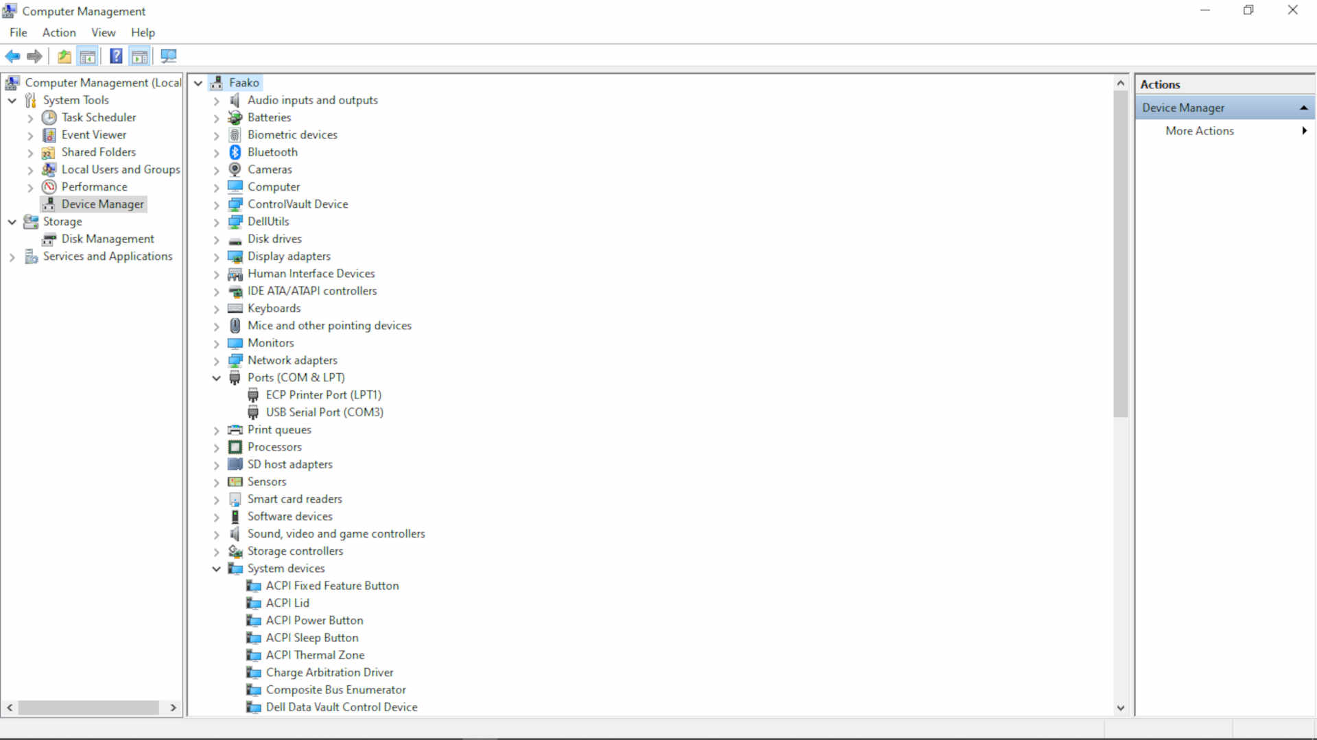 now in my device manager you can now see two devices connected and the programmer is named USB Serial Port(COM3)
Files
What went Worng
A whole lot went wrong with my attempt at the SAMD board, ranging from burnt chips to lossing copper traces to errors from all types of programming methods.
wrapping up
this is a hectic and hard week for me mentally, I was drained but had peace when I switched to the FT232RL board