9. Embedded programming
Welcome to this week’s assignment, this week we will be dealing with setting up and programming our boards to do something. We were tasked individually to read the data sheet for our microcontroller and use our programmer to program our board to do something.
My hello world board was based on an ATtiny 412 microcontroller.
The ATtiny412 Chip
The ATtiny412 used for this Hello board, is a microcontroller using the 8-bit AVR® processor with hardware multiplier, running at up to 20MHz and 4KB Flash, 256B SRAM and 128 bytes of EEPROM in a 8-pin package.
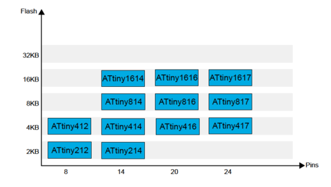 image: tinyAVR®1-Series Overview
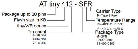 image: Device Designations
However their real capabilities and differences are only understood by thoroughly going through the datasheet - which is huge. I downloaded the datasheet from here - and went through some of the basics of the ATTINY 412.
.jpg)
After cross referencing others material, I found nice comparison between an often confused term - microcontrollers vs microprocessors There can be many comparisons between a PC and a microcontroller - except in the area of multitasking which a computer memory is capable of. However a microcontroller is focused on single task - but also has “thousands (or millions!)” of logic gate circuits and memory.
As it says in the former link, one big question is “Why would it make sense to use a microcontroller to perform a logic function that a small fraction of its constituent gates could accomplish directly? In other words, why would anyone bother to program a microcontroller to perform a digital function when they could build the logic network they needed out of fewer gate circuits?”
Apparently, the answer is quite complex but averaged out as “Ease of configuration and Flexibility”. eg. A single button press can be used to display the time of the day, the no. of times its pressed, light an led, or read the duration.
Likewise, an Arduino is designed for quick prototyping as well as generous amounts of inputs, Outputs and Flash Memory - to see what works and what doesn’t. However the size and dependence on an external computer certainly does not make it a super downscaled “embedded device” to be used in practical contexts such as a mobile phone. It also allows you to take a prototype hobby project “all the way”.
Going through the ATtiny-412 Datasheet
SparkFun tutorial was helpful as it advised on how to approach reading a datasheet. One has to admit that this is an overwhelming exercise as its very difficult to get context of the the technical details and vocabulary - difficult to imagine the context of their use from the descriptions and diagrams alone. It did help me to go through some of the other colleague’s thoughts on this digital bible to get some focus areas.
The four basic blocks of a microcontroller can be broken down as a CPU, Memory, System Clock and Peripherals.
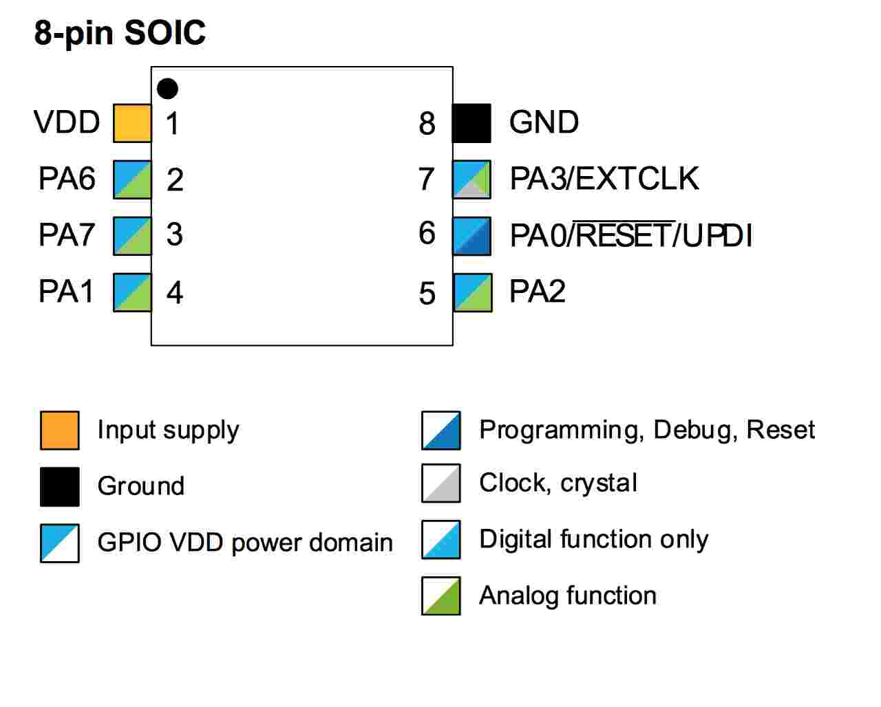 image: Pin out-8-pin SOIC
I tried to gather what all these pin options meant:
| Term | -meaning |
|---|---|
| VCC | Power supply |
| GND | Ground |
| PA | The name for digital pins, which all of these pins are |
| PB | The name for (purely?) analog pins, which the ATtiny412 doesn’t have, but the green indicates an analog functions that five of the pins have. I think this means that they can all do ADC or Analog Digital Conversion |
| RESET | Through this pin you can reset the microcontroller |
| UPDI | Through this pin you can program the board via a UPDI connection - this is linked with the RESET |
| EXTCLK | External Clock Where you can connect this pin to an external clock, such as a resonator |
| GPIO VDD power domain | I wasn’t able to find a clear answer online about what this means, but I think it means that the microcontroller can set a voltage on each of these pins? |
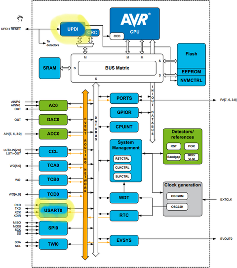 image: ATtiny212 / ATtiny412 Block Diagram
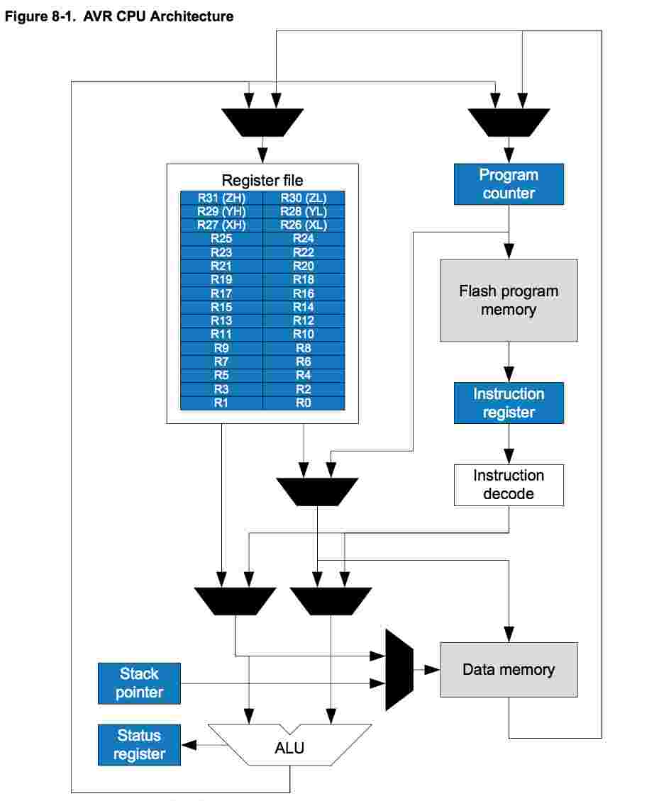 image: CPU work flow
The core features that differentiate it in general are:
A 2/4KB Flash memory, with 128/256bytes of SRAM and 64/128bytes of EEPROM in a 8- pin package
Ideally the programming and instructions for the task are sent through the right pin to the right place at right time - It is to understand this instruction vocabulary that we make use of “[data sheets]”.
.jpg) image: Peripheral Summary of the chip.
image: Peripheral Summary of the chip.
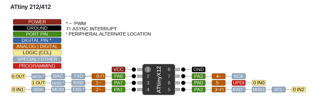 image: Arduino pin out of the Attiny-412 chip
From the Arduino pinout I have a few new pin names, which I think mean the following:
| Term | Meaning |
|---|---|
| MISO(Master In Slave Out) | - Which is the pin to use to send data from the slave to the maser. |
| MOSI(Master Out Slave In) | - Which is the pin to use to send data from the master to the slave / peripherals. |
| SCK (Serial Clock) | -Which are the clock pulses that synchronize data transmission generated by the master. |
| SCL (Serial Clock Line) | -The same as the SCK, but this one is used for an I2C I believe, while SCK is used for SPI communication. |
| SDA -Serial Data | The pin that carries the data when using I2C I think? |
| DAC -Digital Analog Conversion | This allows you to convert digital (numeric) values into analog signals so you can have output voltages that are variable between 0 and 5V, instead of only either 0 or 5V. From the ATtiny412 datasheet there is one DAC pin (PA6, connected to our LED), which is 8-bit. |
| ADC -Analog Digital Conversion | This is doing the reverse from above, where the incoming analog signal is converted into a digital one. This has to be in steps, and the higher the number of steps, the higher the resolution. With a 10-bit ADC you can detect 1024 (being 2^10) discrete analog levels, while 8-bit can detect 256 (2^8) discrete levels. If I understand the ATtiny datasheet correctly (from the Peripheral Summary), then all 6 (non VCC/GND) pins are ADC (at 10-bit 115ksps). |
| TXD -Transmit | The transmitting pin to do serial communication (UART or USART I think? Which is serial over USB). |
| RXD -Receive | The receiving pin to do serial communication. |
there are a few extra marks, such as the tilde (~) meaning a PWM pin (Pulse Width Modulation), which I’ll get to in the fading LED example below, and the alternate locations of the TXD, RXD and MOSI, MISO which I’d already discovered during my testing, because our board is making use of these alternate positions. I’m not quite sure what the async interrupt truly means.
My Hello Board
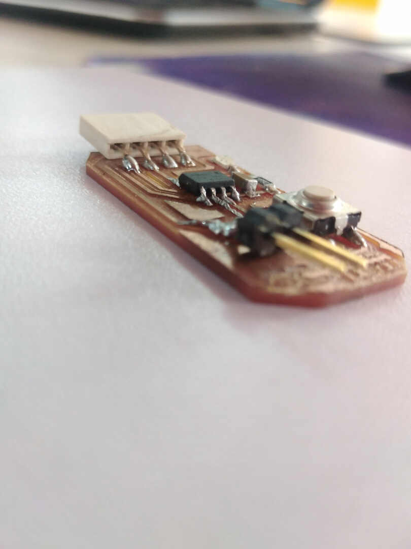 .
So this week, I used my board from the week07 assignment for this week’s Embedded programming assignment. I chose to use the arduino environment to programe my board. you can visit my week07 to learn how to setup the arduino environment and the DTECH USB to UART TTL cable with your board.
.
So this week, I used my board from the week07 assignment for this week’s Embedded programming assignment. I chose to use the arduino environment to programe my board. you can visit my week07 to learn how to setup the arduino environment and the DTECH USB to UART TTL cable with your board.
I worte three programs for my board, namely - an LED blink program, an LED fade program and an LED-button controlled program.
LED blink program
So from the Attiny-412 datasheet, I found out the right pin my LED was connected to is PA6 which equates to digital pin0 in arduino. So with this in mind I set out to write my code and initialize that LED at pin0, I set the LED pin to an output and I delayed the switch for a second.
int LED = 0;

void setup(){
    pinMode(LED, OUTPUT);
}
void loop(){
    digitalWrite(LED, HIGH);
    delay(1000);
    digitalWrite(LED, LOW);
    delay(1000);
}
Blink Test
The LED Fade program
There is a handy Fading Example on the Arduino website that uses this PWM technique, using the analogWrite function (instead of the digitalWrite function from the “blink” example). The analogWrite function can take integers between a value of 0 - 255, where the higher, the brighter the LED should become.
However, I noticed that the pin that our LED is connected to, pin PA6 does not have PWM. Another sad by-effect from having switched the TX and RX pins. Using the analogWrite function, and the “fade” example therefore didn’t work. I compiled and uploaded it, but my LED remained off.
I therefore had to mimic a PWM through purely software means. This is done by using the digitalWrite function combined with the delay to basically create your own pulses. You make your own pulses of width X milliseconds long, and using the digitalWrite you turn it on for, say 20% of the time of that pulse and off for the remaining 80% of the time of a pulse.
I definitely needed a first starting example to wrap my head around it, but eventually it clicked and I understood what was happening and adjusted the examples to my own version:
// Using "software PWM" to fade my LED
// Loosely based on: https://forum.arduino.cc/index.php?topic=104572.0

const int led_pin = 0;
float steps = 25; // The max time of each step
float fade_step = 0.5;
// It takes (steps / fade_step) steps to go from OFF to ON
// the "delay()" function should take "unsigned long"
// but I really need 0.5 milliseconds or less
// and using the delayMicroSeconds() doesn't work,
// because it can't handle numbers above a few thousand microseconds
// which is only a few milliseconds

void setup() {
  Serial.swap(1); //Because I have swapped TX/RX pins
  pinMode(led_pin, OUTPUT);
}//void setup

void loop(){
  // Fade to bright | Runs from 0% -> 100%
  for(float i = 0; i <= steps; i += fade_step) {
    digitalWrite(led_pin, HIGH);
    delay(i);         // ON for this long
    digitalWrite(led_pin, LOW);
    delay(steps - i); // OFF for this long, the remaining "pulse width"
  }//for

  // Stay on for a while
  digitalWrite(led_pin, HIGH);
  delay(50);

  // Fade to dim | Runs from 100% -> 0%
  for(float i = steps; i >= 0; i -= fade_step){
    digitalWrite(led_pin, HIGH);
    delay(i);
    digitalWrite(led_pin, LOW);
    delay(steps - i);
  }//for

  // Stay off for a while
  digitalWrite(led_pin, LOW);
  delay(50);
}//void loop
As you ca see here
The LED-Button Program
Now with the button, I found out that it was connected to pin 4 with the help of the pinout from the datasheet. So I initialize both the LED and Button at pin 0 and pin 4 respestiviely. I initialize the buttonstate to be zero(0), I set the pinMode for the LED as output and for the button as input but I had to add Pullup to the input since the ATtiny-412 has an internal pillup resistor. I did this to correct some mishaps when I test tested the program at first. I used and if-else condition in the program. see the code below
const int buttonPin = 4;     // the number of the pushbutton pin
const int ledPin =  0;      // the number of the LED pin

// variables will change:
int buttonState = 0;         // variable for reading the pushbutton status

void setup() {
  // initialize the LED pin as an output:
  pinMode(ledPin, OUTPUT);
  // initialize the pushbutton pin as an input:
  pinMode(buttonPin, INPUT_PULLUP);
}

void loop() {
  // read the state of the pushbutton value:
  buttonState = digitalRead(buttonPin);

  // check if the pushbutton is pressed. If it is, the buttonState is HIGH:
  if (buttonState == LOW)
   {
    // turn LED on:
    digitalWrite(ledPin, HIGH);
  } else {
    // turn LED off:
    digitalWrite(ledPin, LOW);
     }
}
Watch the video
Group work
compare the performance and development workflows for other architectures. The table below shows the comparison between AVR and ARm architectures and in my case I used an AVR architecture based chip AT-tiny 412.
| AVR | ARM |
|---|---|
| AVR micro controller refers to Advanced Virtual RISC (AVR). | ARM micro controller refers to Advanced RISC Micro-controller (ARM). |
| It has bus width of 8 bit or 32 bit. | It has bus width of 32 bit and also available in 64 bit. |
| It uses ART, USART, SPI, I2C communication protocol. | It uses SPI, CAN, Ethernet, I2S, DSP, SAI, UART, USART communication protocol. |
| Its speed is 1 clock per instruction cycle. | Its speed is also 1 clock per instruction cycle. |
| Its manufacturer is Atmel company. | Its manufacturer is Apple, Nvidia, Qualcomm, Samsung Electronics and TI etc. |
| It uses Flash, SRAM, EEPROM memory. | It uses Flash, SDRAM, EEPROM memory. |
| Its family includes Tiny, Atmega, Xmega, special purpose AVR. | Its family includes ARMv4, 5, 6, 7 and series. |
| It is cheap and effective. | It provides high speed operation. |
The table below shows the configuration of the AT-tiny 412 which is being compared to the Atmel SAMD11C14A Chip
| AT-tiny 412 | |
|---|---|
| Pins | 8 |
| SRAM | 256B |
| Flash | 4KB |
| EEPROM | 128B |
| Max. frequency (MHz) | 20 |
| 16-bit Timer/Counter type A (TCA) | 1 |
| 16-bit Timer/Counter type B (TCB) | 1 |
| 12-bit Timer/Counter type D (TCD) | 1 |
| Real Time Counter (RTC) | 1 |
| USART | 1 |
| SPI | 1 |
| TWI (I2C) | 1 |
| ADC | 1 |
| ADC channels | 6 |
| DAC | 1 |
| AC | 1 |
| Custom Logic/Configurable Lookup Tables | 1 |
| Window Watchdog | 1 |
| Event System channels | 6 |
| General purpose I/O | 6 |
| External interrupts | 6 |
| CRCSCAN | 1 |
| SAMD11C14A | |
|---|---|
| Pins | 14 |
| General Purpose I/O-pins (GPIOs) | 12 |
| Flash | 16KB |
| SRAM | 4KB |
| Timer Counter (TC) | 2(3) |
| Waveform output channels for TC | 2 |
| Timer Counter for Control (TCC) | 1 |
| Waveform output channels per TCC | 8 |
| DMA channels | 6 |
| USB interface | 1 |
| Serial Communication Interface(SERCOM) | 2 |
| Analog-to-Digital Converter (ADC)channels | 5 |
| Analog Comparators (AC) | 2 |
| Digital-to-Analog Converter (DAC)channels | 1 |
| Real-Time Counter (RTC) | Yes |
| RTC alarms | 1 |
| RTC compare values | 1 32-bit value or 2 16-bit values |
| External Interrupt lines | 8 |
| Peripheral Touch Controller (PTC)channels (X- x Y-lines) for mutual capacitance | 12 (4x3) |
| Peripheral Touch Controller (PTC)channels for self capacitance (Ylines only) | 7 |
| Maximum CPU frequency | 48MHz |
| Packages | SOIC |
| Oscillators | 32.768kHz crystal oscillator (XOSC32K) 0.4-32MHz crystal oscillator (XOSC) 32.768kHzinternal oscillator (OSC32K) 32kHz ultra-low-power internal oscillator (OSCULP32K)8MHz high-accuracy internal oscillator (OSC8M) 48MHz Digital Frequency Locked Loop (DFLL48M) 96MHz Fractional Digital Phased Locked Loop (FDPLL96M) |
| Event System channels | 6 |
| SW Debug Interface | Yes |
| Watchdog Timer (WDT) | Yes |
wrapping Up
This was a really good week for me, I didn’t face any problems and every thing worked accoring to plan.