7. Electronics design
In this week’s Electronics design assignment, I worked on designing my own PCB traces, milling it out with a table top CNC machine, soldering the necessary components onto the finished PCB and programmed it with a simple blink program. I will take you through the process I went through, the ups and downs of this week assignment.
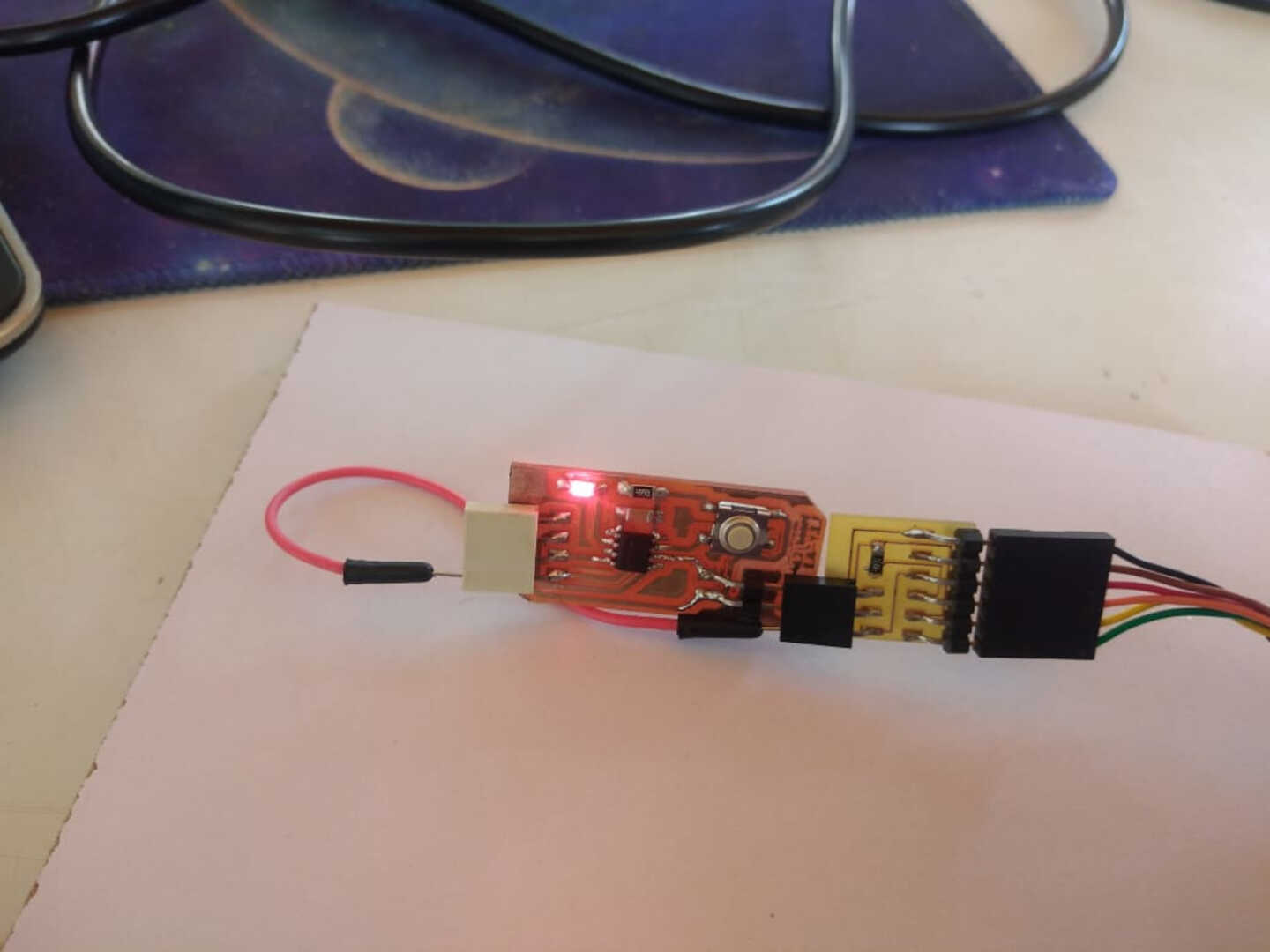
Hero shots
The tasks for this week
group project: use the test equipment in your lab to observe the operation of a microcontroller circuit board individual project: redraw an echo hello-world board, add (at least) a button and LED (with current-limiting resistor) check the design rules, make it, and test that it can communicate extra credit: simulate its operation
Group Assignment
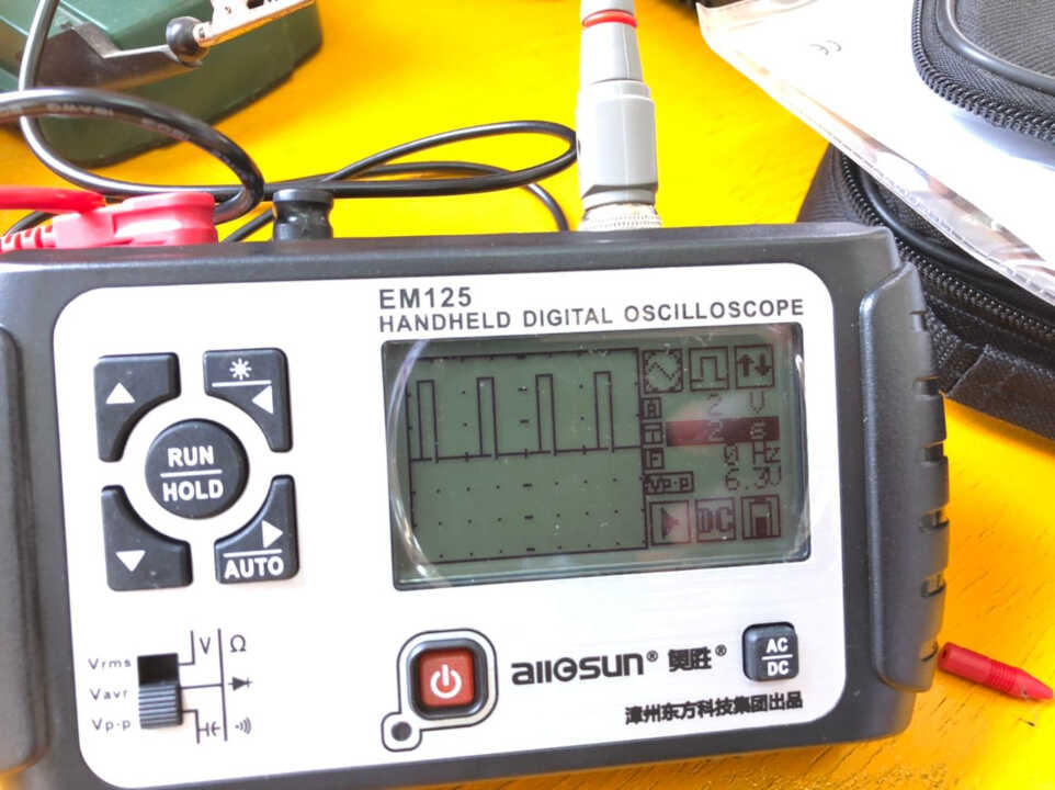
This week’s group’s task involved using test equipment in the lab to observe the operation of a microcontroller circuit board using an oscilloscope and voltmeter. This week we used the equipment to check the final circuit board created for one of the boards produced.
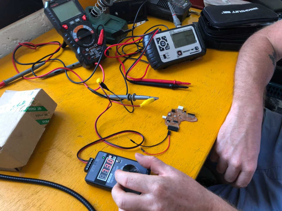
We used the small voltage generator to power the different current sources on the board (9v and 5v).With the multimeter we could test the components such as the capacitor, the led, the linear regulator, the button and the continuity between the pins. After these different tests, we uploaded a flashing program of the led on the board and thanks to the oscilloscope we have to observe the digital signal at the output. The image below shows the results in on the oscilloscope used.
 .
.
Individual assignment
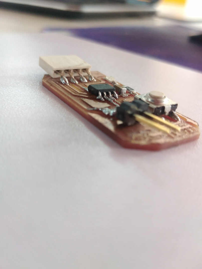
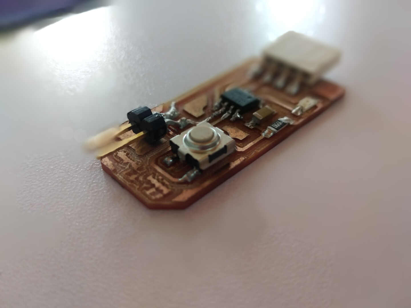
I will be working on designing and programming a UPDI Hello-world board based on the AT-tiny 412 chip. I did all my PCB schematics using KiCAD 6.0. It is a blink board which has seven(7) comoponents in total.
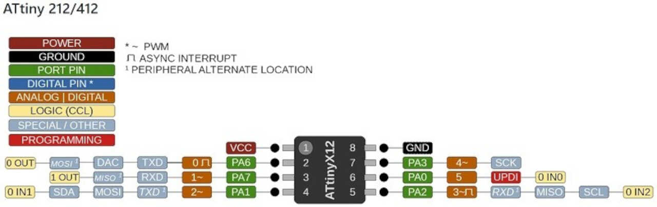
AT-tiny 412 pinout
Libraries
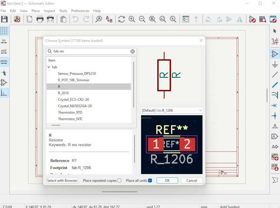
To begin with the design of my hello_world board, I had to add several symbol and footprint libraries to the KiCAD libraries. Specifically the Fab Electronics Library for KiCad that contains the symbols and footprints of (almost) all the parts that we’ll be using during the Academy.
For the installation process I recommend this video that was really useful to me, created by Fab Academy’s Kris of Aalto Fab. This video makes the addition of libraries way easier and simple.
Symbols Schematic
This picture shows the 2D schematic of the circuit in the KiCAD Schematic editor. The arrangements and cnnections of the various components are made in this editor window of the KiCAD software.
Now after adding all the necessary libraries, I used the already existing tools to add symbols to the work space.
 this image shows it. after adding the symbols,
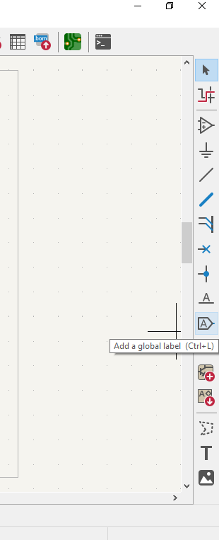
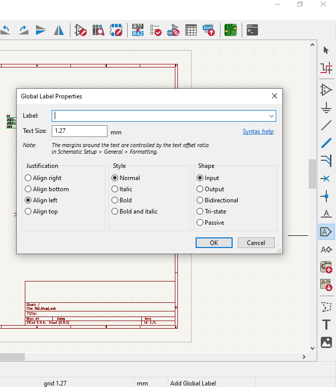
- you can add net functions to all the terminals of your symbols by using the add net label tool.
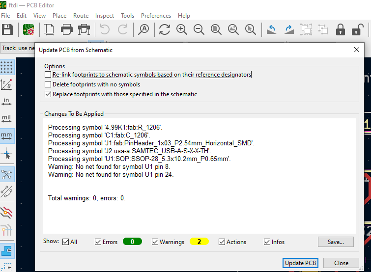
 When I was done with placing my symbols and rearranging them, this is what I had down below. I exported a Netlist so I can use it do generate a PCB in the PCB editor.

-
I clicked the open in PCB editor tool on the menu tool bar.

-
Now in the PCB editor, you can either import the Netlist you exported in the schematics window or yoou can use the shortcut key.
-
I prefer using the shortcut Key [F8]. When you press [F8] it will autmatically pick up the symbols in the schematic window and update your PCB editor work space with it.
 you can move the footprints to places and alignment of your choice.
Now this was my strategy I used to lay my traces without any problem
This below shows the circuit in the KiCAD PCB editor window with the footnotes of the symbols used in the Schematic editor and the copper traces that does the connections.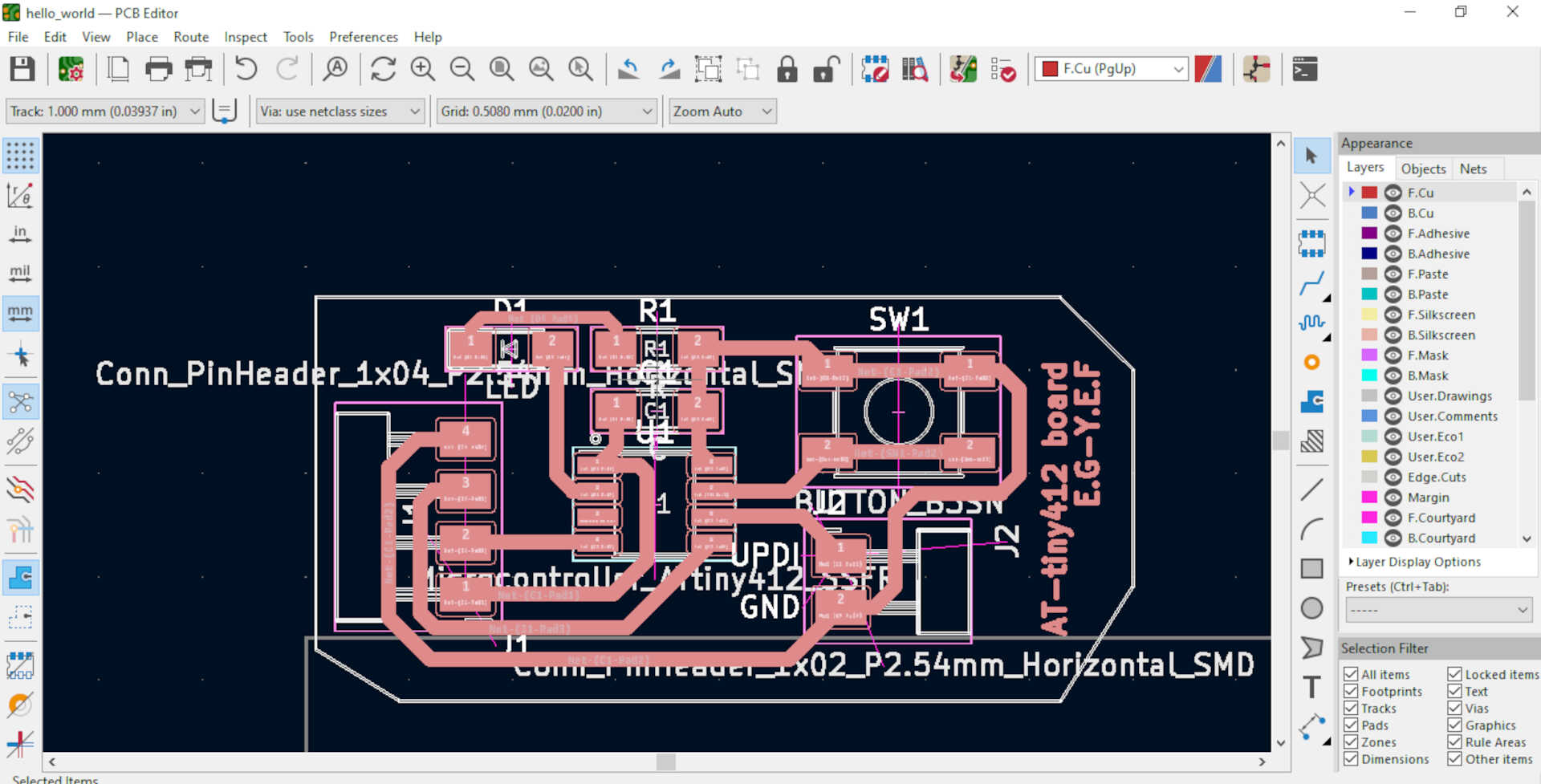
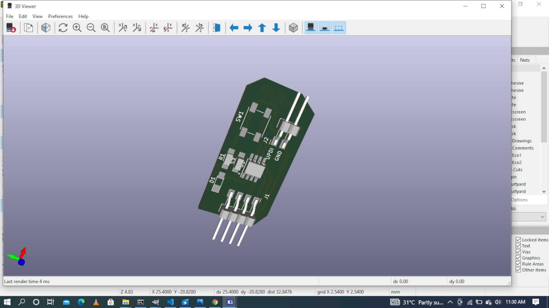
3D View of the Circuit
These picture below shows the three dimensional(3D) view of the complete circuit with the components used in the KiCAD 3D viewer window.

PRDUCTION
Now, this the production stage of the assignment. The PCB was milled out on the Table top CNC machine I used in week 4 with the same tool diameter, cut depth, feed rate and spindle speed. After the board was designed, I exported it as a Gerber file using the export option in KiCAD.
Component list
- 1 capacitor(1uf) SMD
- 1 5k ohm resistor SMD
- 1 AT-tinyMega 412 chip
- 1 lED
- 1 button
- 1 male jtag 1x2 connector
- 1 female jtag 1x4
The image below shows the copper traces in the CNC software and the tool path it will follow.

this image shows the list of components and the milled out PCB board for the assignment

Soldering
These pictures shows the initial stage of the soldering process and the final stage of the soldering stage.
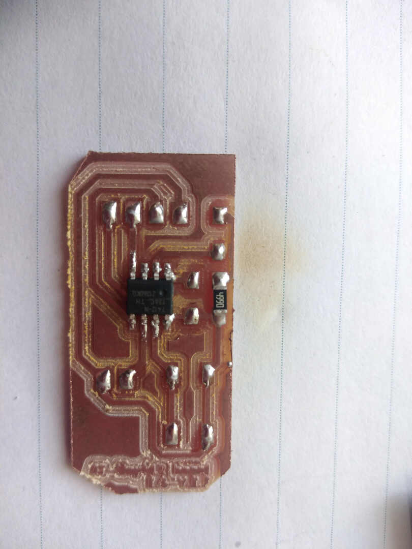 Image: First stage
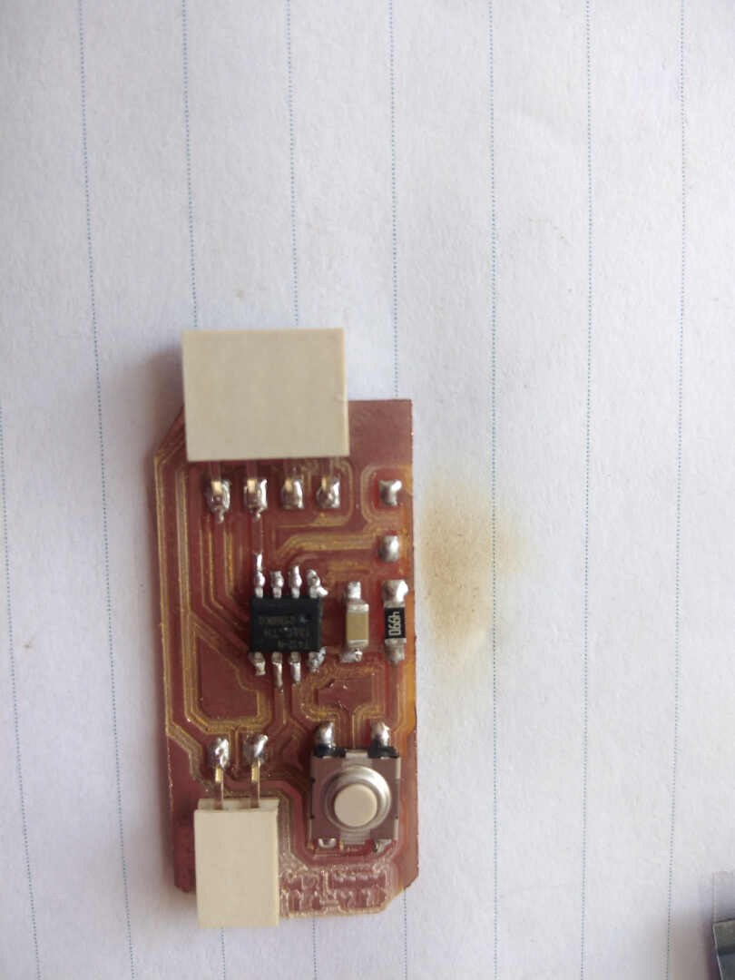 Image: Final stage
Programming
Now this is where I experienced the downs I talked about. I used the Arduino IDE to program my hello-world UPDI board. Now the FTDI programmer I could not be reached by the arduino software.
so I had to use a DTECH USB to UART TTL cable to connect the Hello-world UPDI board to my laptop computer to program it.
 .
.
You can find the pinout connection of the DTECH USB to UART TTL cable here.
Now in the Arduino IDE you need to download and install the MegaTiny core library. But before you do that you need to set your preferred other websites for download of libraries in the arduino IDE.

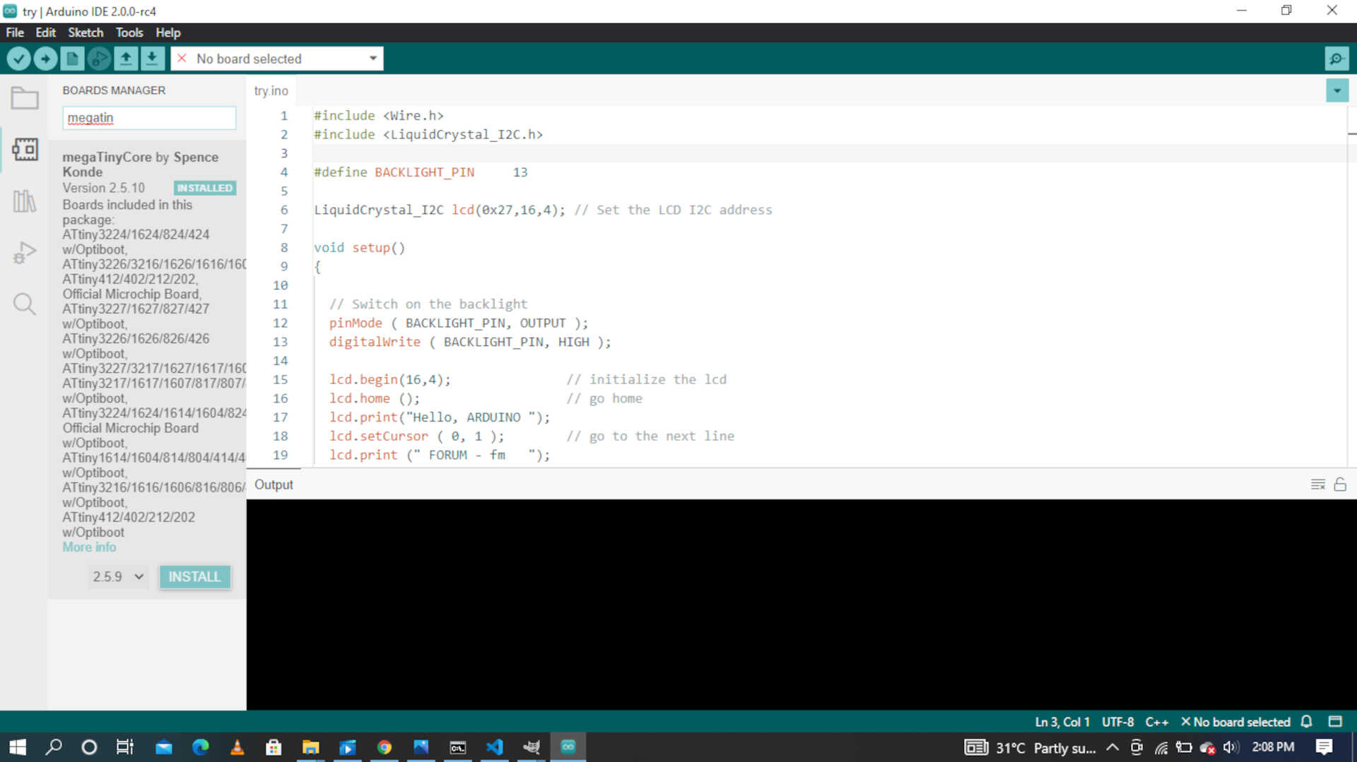 Image: download the MegaTiny core library.
Problems
So I faced a single problem and that was getting the Arduino IDE to upload to the micro-controller. It always returned an error saying unable to reach the programmer. So i fixed this by adding the MegaTiny-core library to arduino and set the programmer. you can find the process of setting the programmer below in the section.
Setting the parameters for the board.
I had to experiment with the parameters in the tools tab for a while to find the ideal paramters to enble me to program my board with sucess.
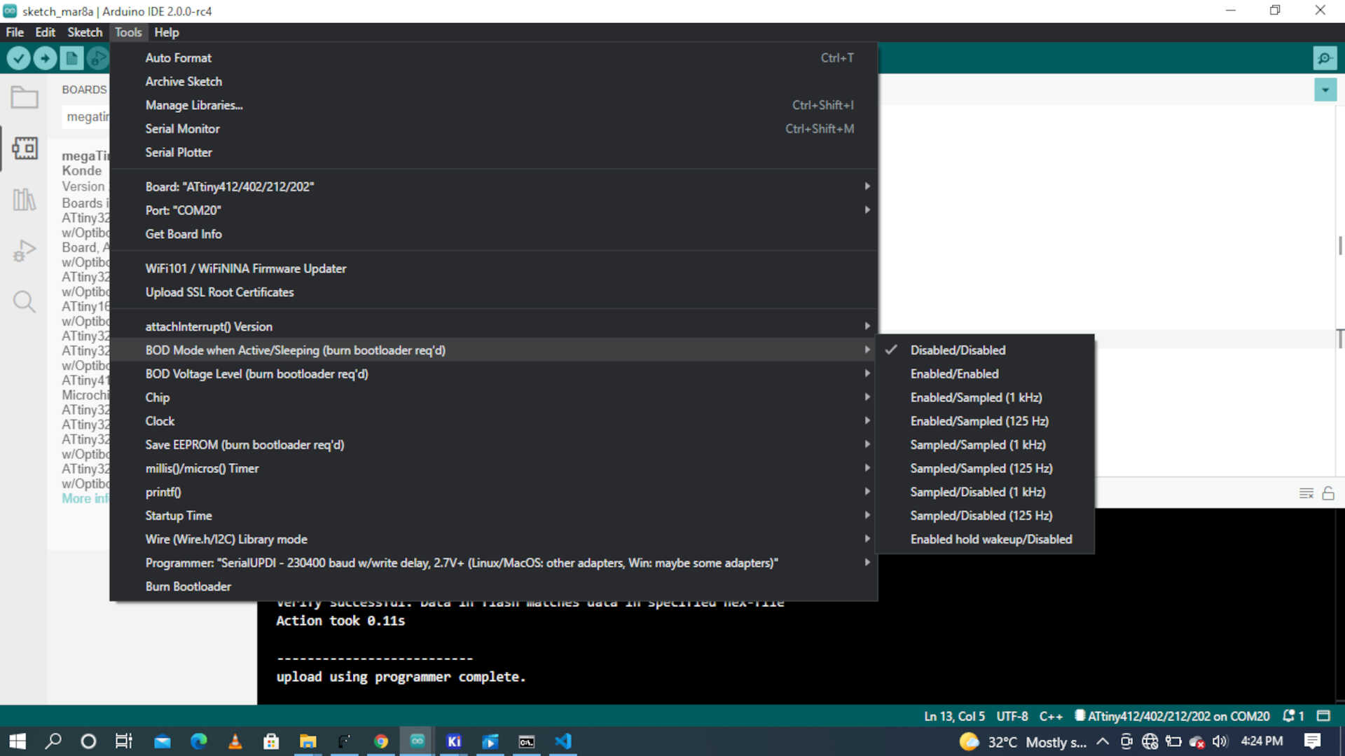 image: BOD mode
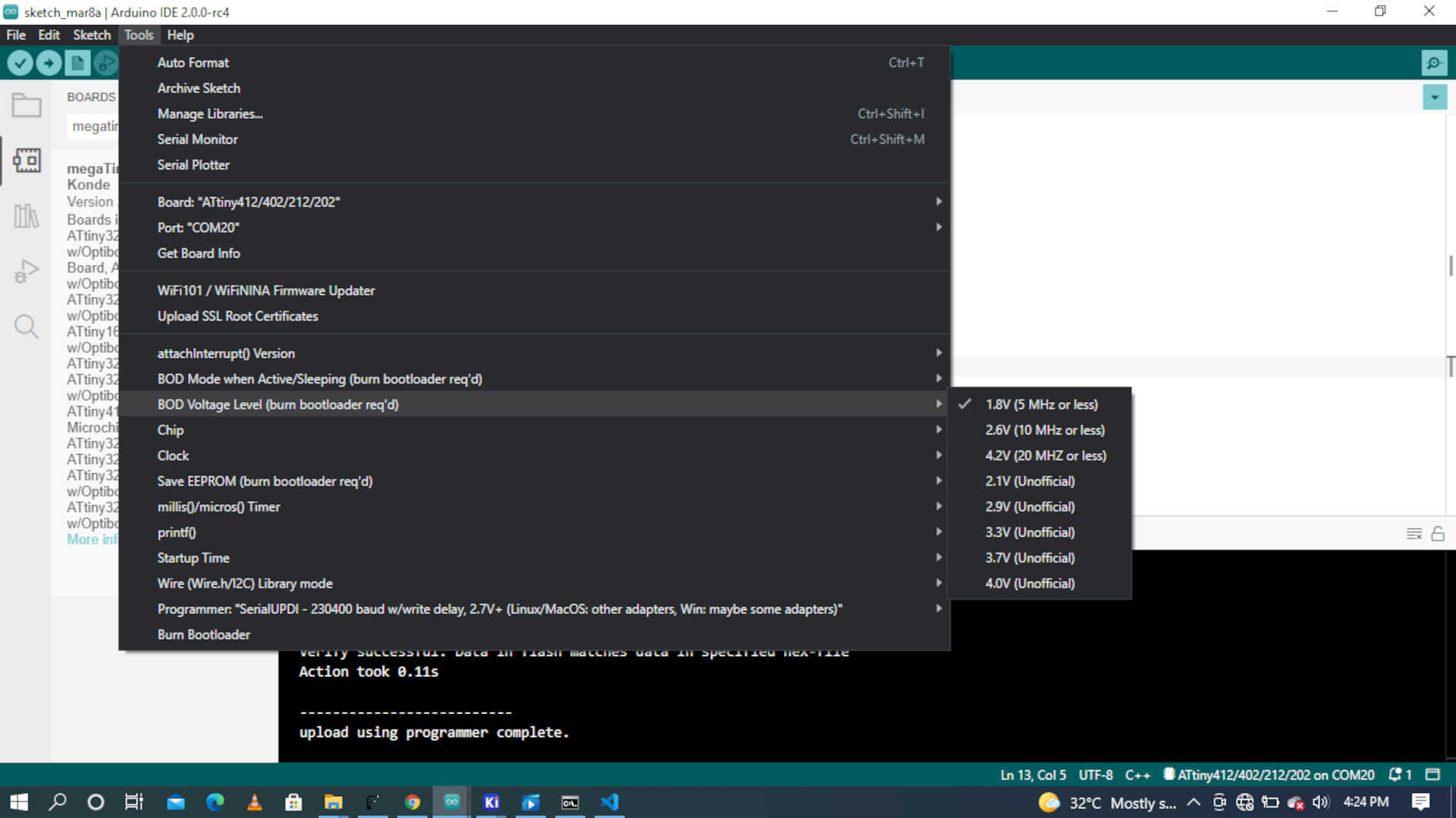 image: BOD voltage level
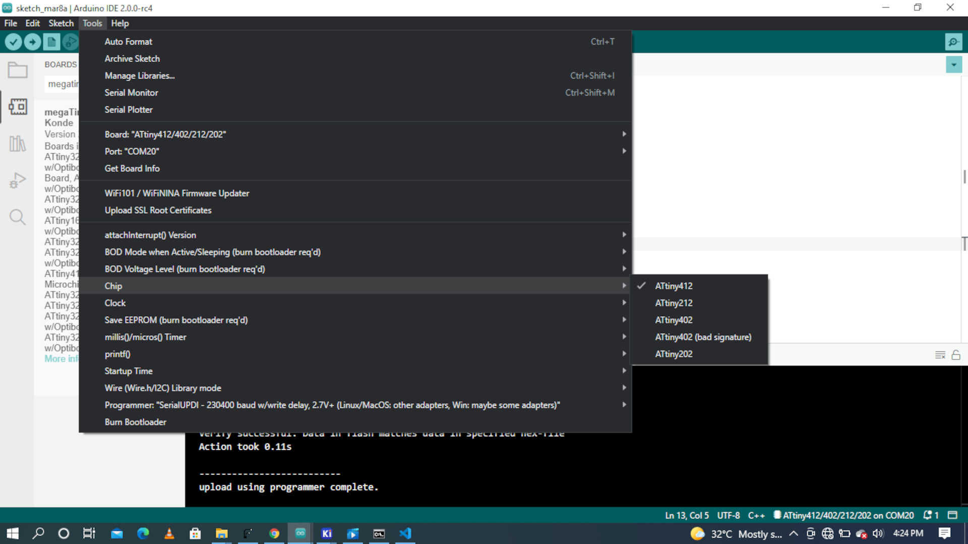 image: Chip selection
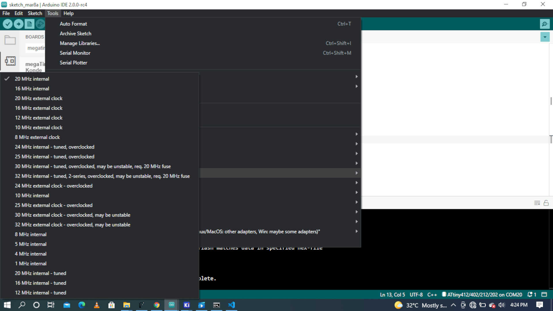 image: Clock setting
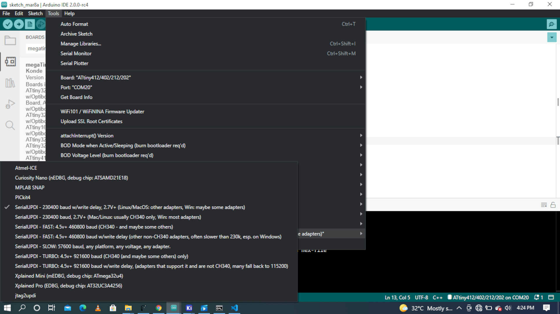 image: Programmer selection
.ino file
int pin = 0;
int del = 1000;

void setup() {
Serial.begin(9600);
pinMode(pin, OUTPUT);
}

void loop() {
 digitalWrite(pin, HIGH);
 Serial.println("ON");
 delay(del);
 digitalWrite(pin, LOW);
 Serial.println("OFF");
 delay(del);
}
Files
What when wrong?
etting the Arduino IDE to upload to the micro-controller.
What went well
basically every thing except the uploading the code at first but i fixed that.
What would I do differently next time?
change the overall design of my board to an intriguing one.
wrapping Up
this was a new and exciting experience to me. My first ever programmed board.