
This work is licensed under a Creative Commons Attribution-NonCommercial-ShareAlike 4.0 International License
Week 4: Electronics Production
Feb 23, 2021Summary
This week's assignments
- Group assignment:
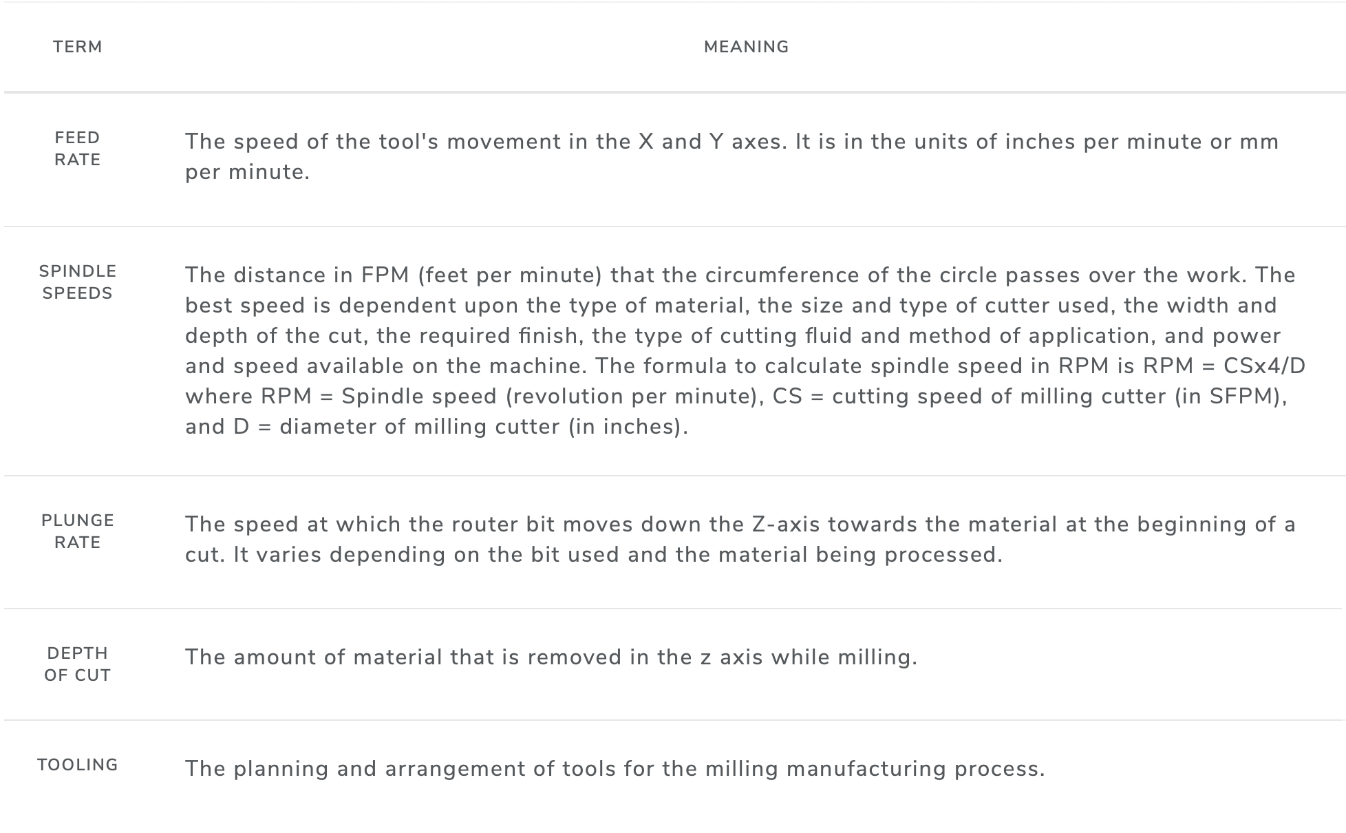
- Characterize the design rules for your PCB production process: document feeds, speeds, plunge rate, depth of cut (traces and outline) and tooling ✔
- Document your work (in a group or individually) ✔
- Individual assignment:
- Make an in-circuit programmer by milling and stuffing the PCB, test it, then optionally try other PCB fabrication process:
- Document how you made (mill, stuff, solder) the board ✔
- Document that your board is functional ✔
- Explain any problems and how you fixed them ✔
- Includ a "hero shot" of your board ✔
Resources Used
- Website / Software: mods - cba edition
- Hardware: Roland SRM-20
Skills Gained
- PCB Milling, Soldering, "Smoke Test" and "Continuity Test"
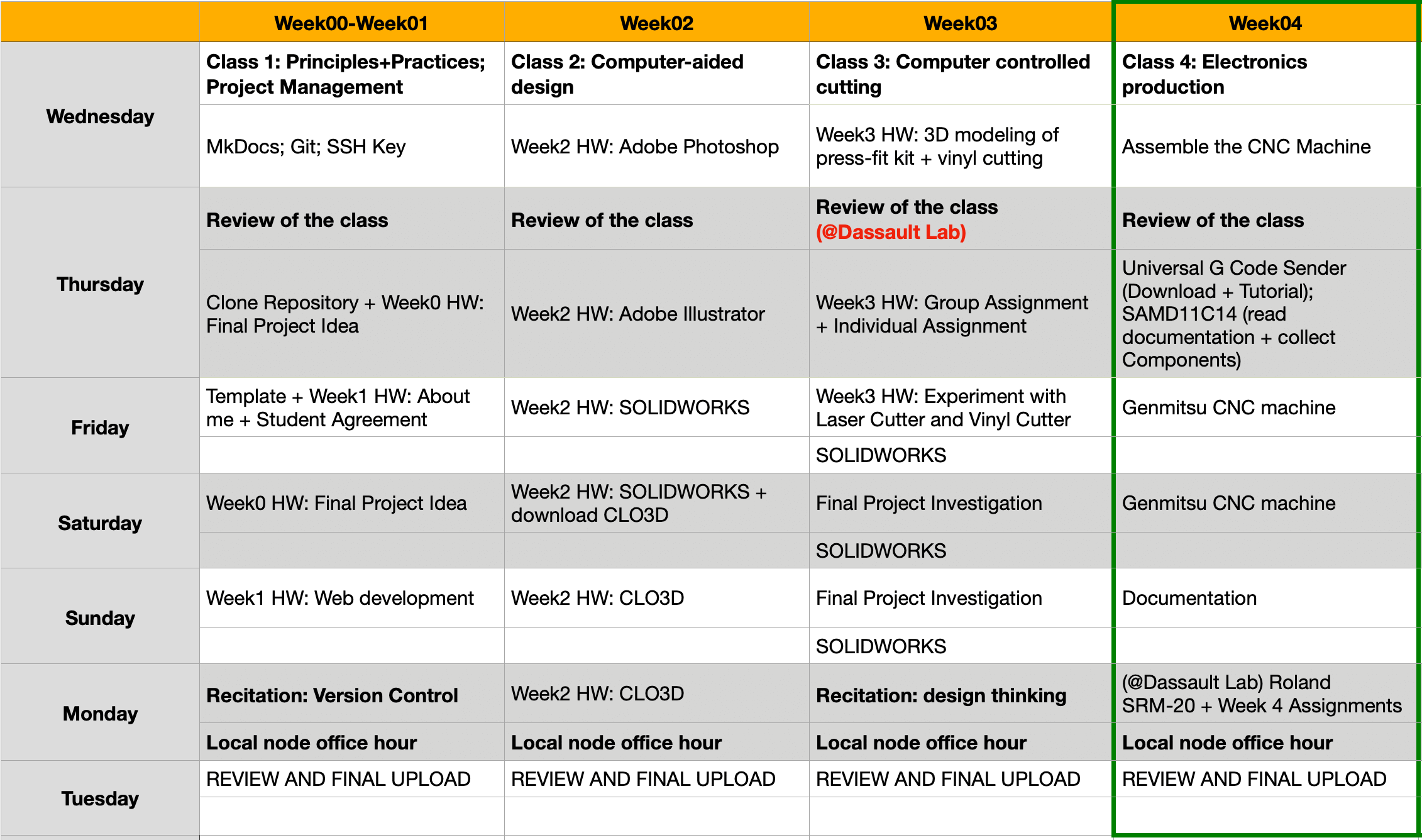
My Weekly Schedule
Assembling and Setting up the Genmitsu 3018 Machine
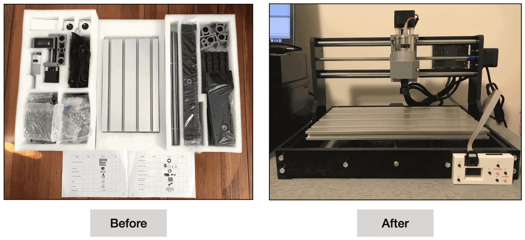
In response to the ongoing COVID-19 pandemic, each of us at the 3DEXPERIENCE Lab received a Home Fab Lab Kit at the beginning of the course to complete the majority of the assignments from our homes. The Home Fab Lab Kit consisted of an FDM 3D Printer, a desktop CNC router, and an electronics production kit including a soldering station, fume extractor, multimeter, hand tools, accessories, consumables and electronic components.
The PCB milling machine that we received was the Genmitsu CNC Router 3018-PRO, it was carefully packaged and was easy to assemble thanks to the clear instruction manual. There were some sharp edges and corners so I must be very careful. Nonethless, it was a smooth process and seemed to be a great PCB milling machine to a beginner like me!
The PCB milling machine can be controlled by a remote controller (the white board on the front in the above image), or by a G code software. Since the G code software (Candle) that came with the machine only worked on Windows operating system, our instructor Spencer recommended us an alternative open-source G code platform (Universal Gcode Sender) that works for Mac.
At first I was unable to install / open Universal Gcode Sender because I kept receiving an error message when double clicking the icon, and so I installed another G code software (Bantam Tools), but then I realized that Bantam Tools only worked for its licensed products.
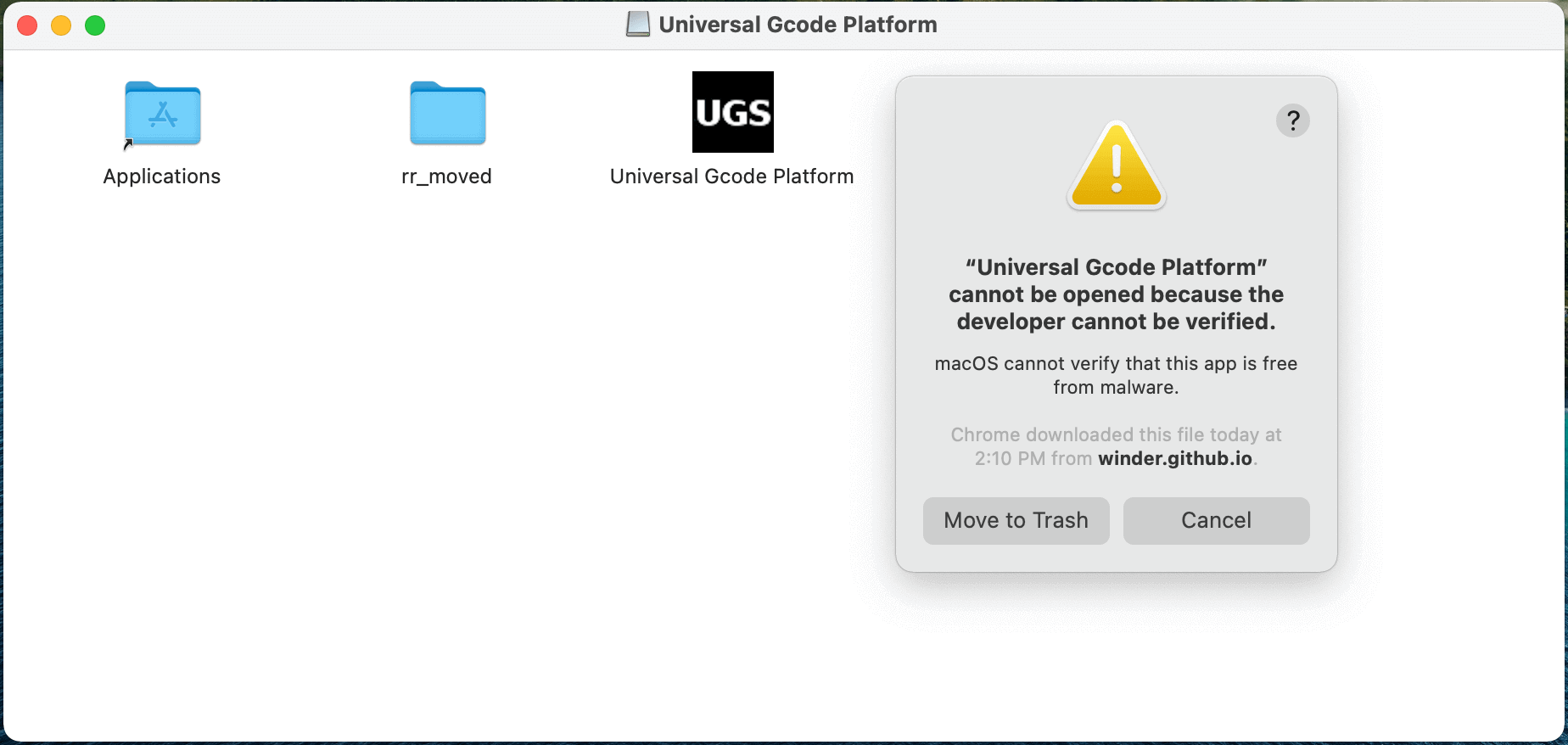
Instead of searching for another new G code software, I decided to revisit the error message that I received previously and searched online for possible resolutions. To my surprise, I was not the only one who encountered this error, and thankfully, the macOS User Guide had clear instruction on how to resolve this issue, and it worked!
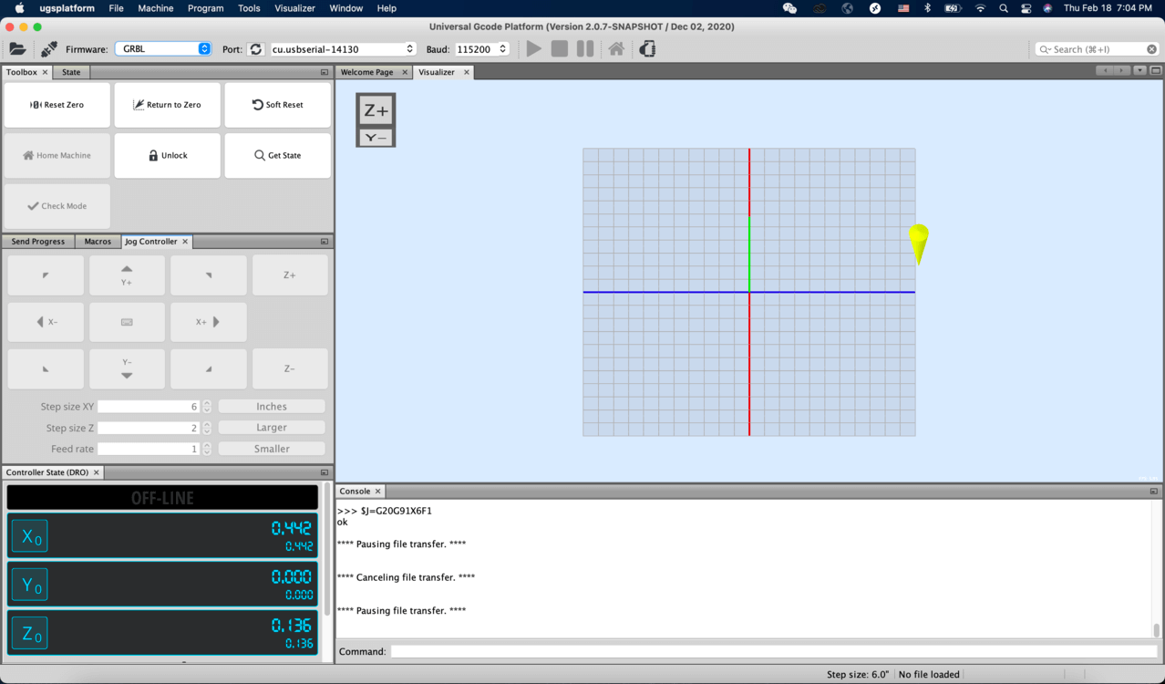
Compared to the remote controller, I found that the G code platform had more flexiblity for the adjustment of the step settings, so I was able to make the step size to be very small and this would be helpful especially when zeroing the z-axis; yet the remote controller was a nice bonus as it didn't require connection to my computer. One thing that I must remember is not to connect the PCB milling machine to both the remote controller and Universal Gcode Sender (via USB) at the same time, because this would confuse the machine.
Here is a video of me controlling the machine via the remote controller.
Here is a video of me controlling the machine via Universal Gcode Sender. In the video, I set the "Step Size XY" to 2 mm, and moved the chunk / spindle along the +X direction in micro steps.
I spent the weekend to learn the machine, however, one downside of the machine was that it did not have an enclosure and thus the noise was inevitable 😅. In order to be able to complete my assignments in time without affecting my neighbors, I have joined my classmate Jonathan and our instructor Spencer to learn the Roland SRM-20 milling machine at the lab on Monday and completed majority of this week's assignments there.
Group Assignment: Characterizing the Machines
Introduction
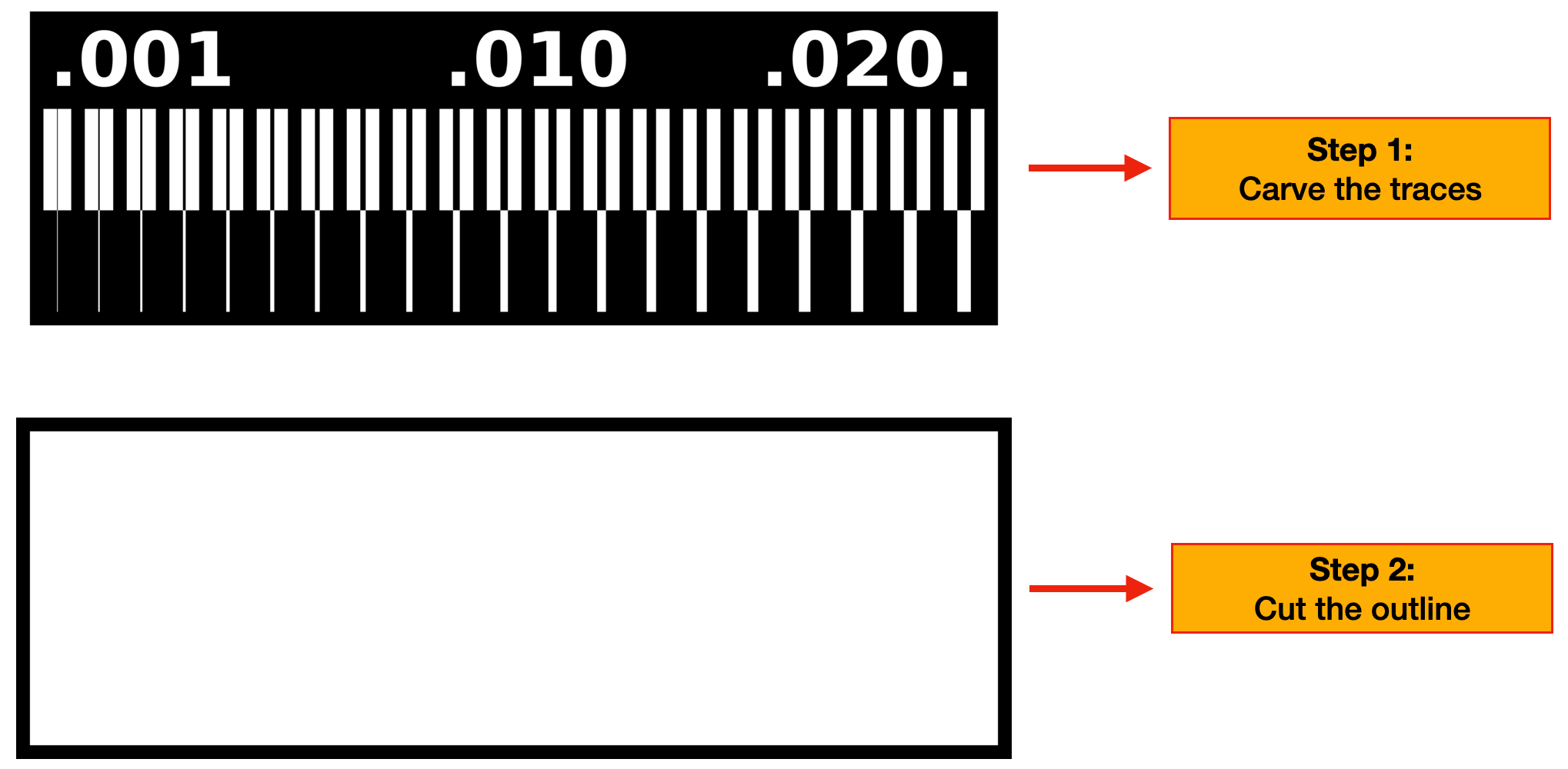
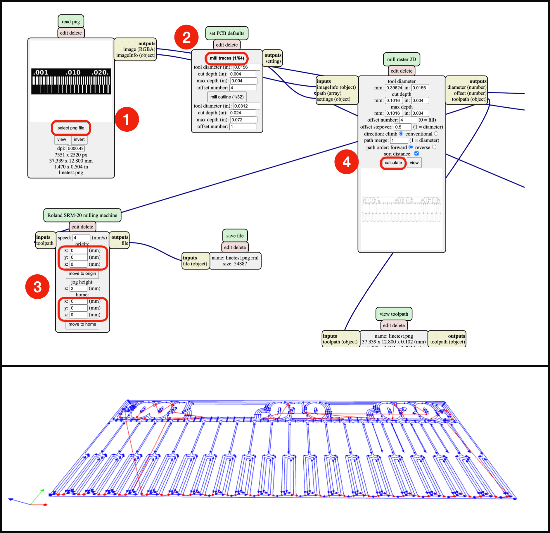
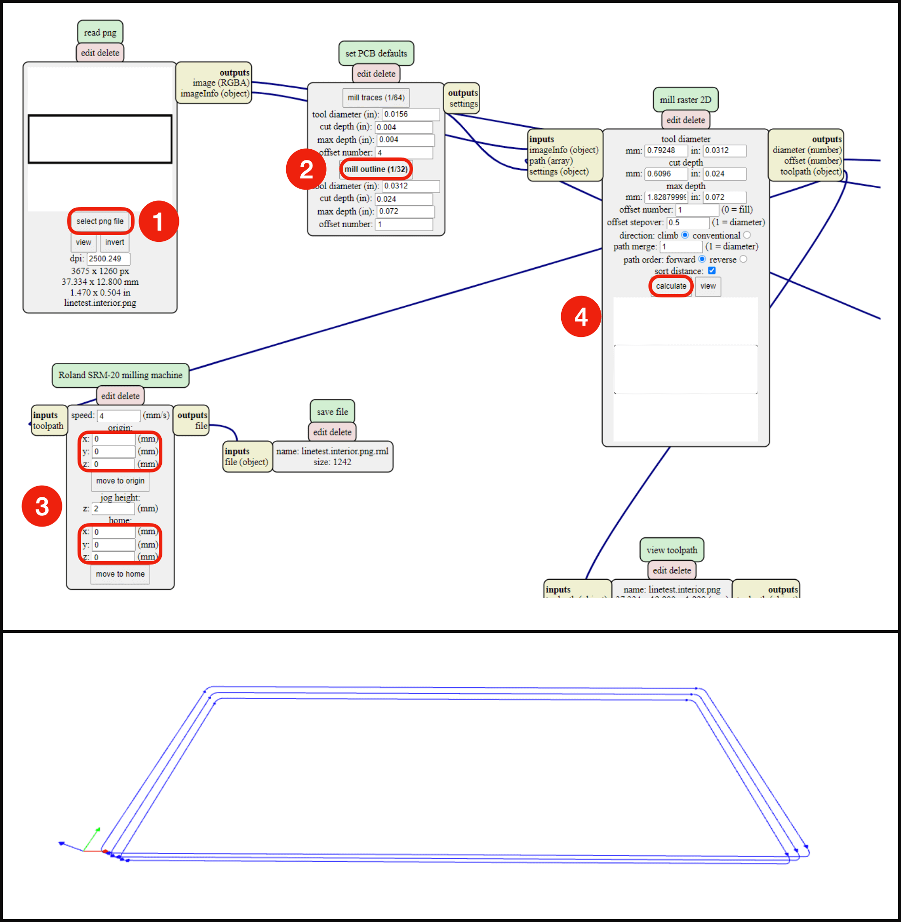
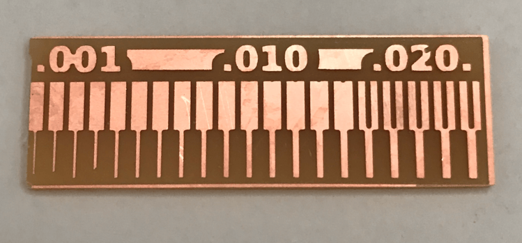
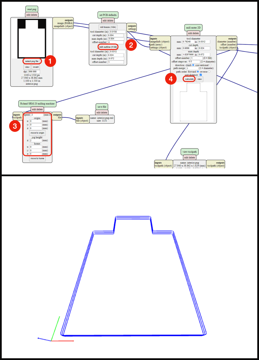
The group assignment this week was to characterize the design rules for our PCB production process. Specifically, we were to carve the traces of precision test file using the 1/64" (0.4 mm) bit, and cut the outside profile of the file using the 1/32" (0.8 mm) bit on an FR1 board. The image below shows the traces file and the outline file that I used to characterize the machine. The white area was where we wanted to leave, and the black area was where we wanted the machine to cut away as much as possible.
Generating the G-Code Files
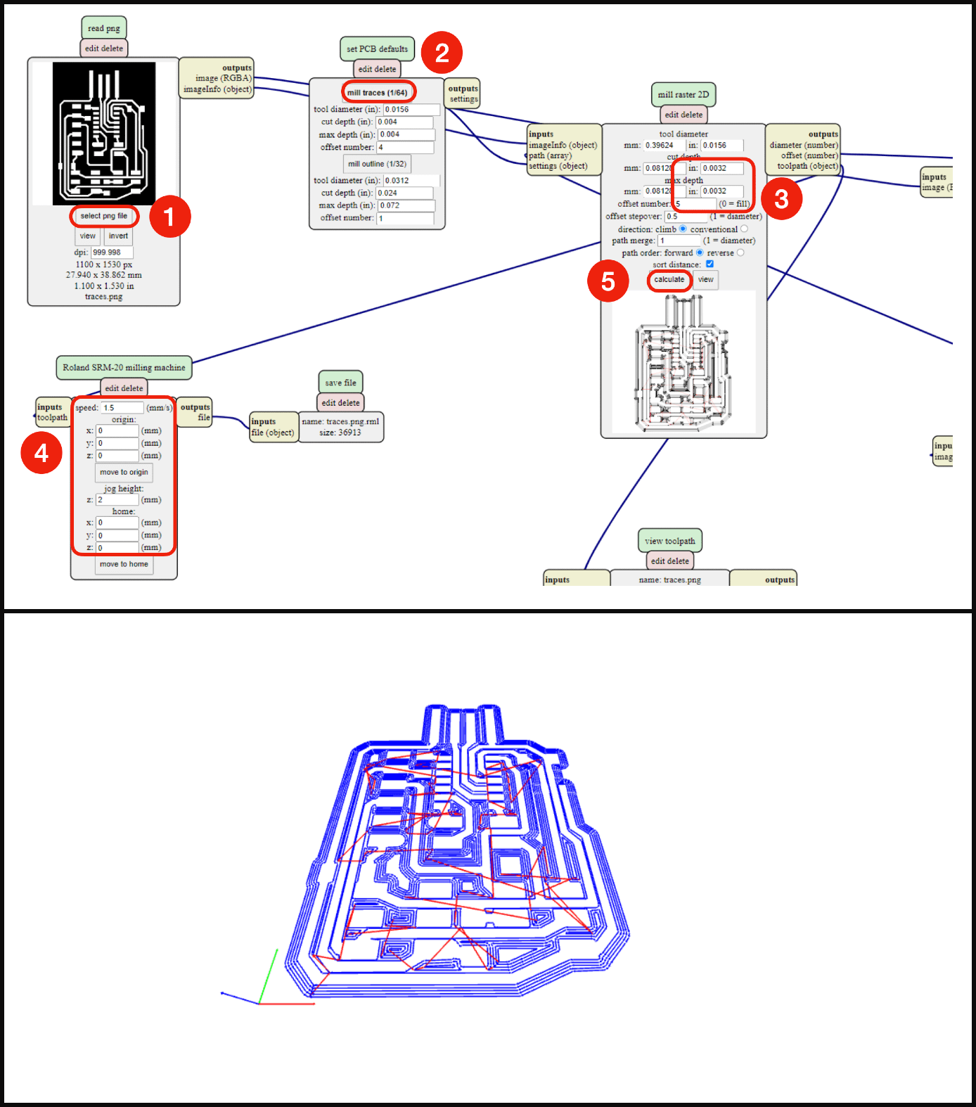
We used mods to generate the G code. The program that we used was the Roland SRM-20 / PCB png program under the open serve program selection.
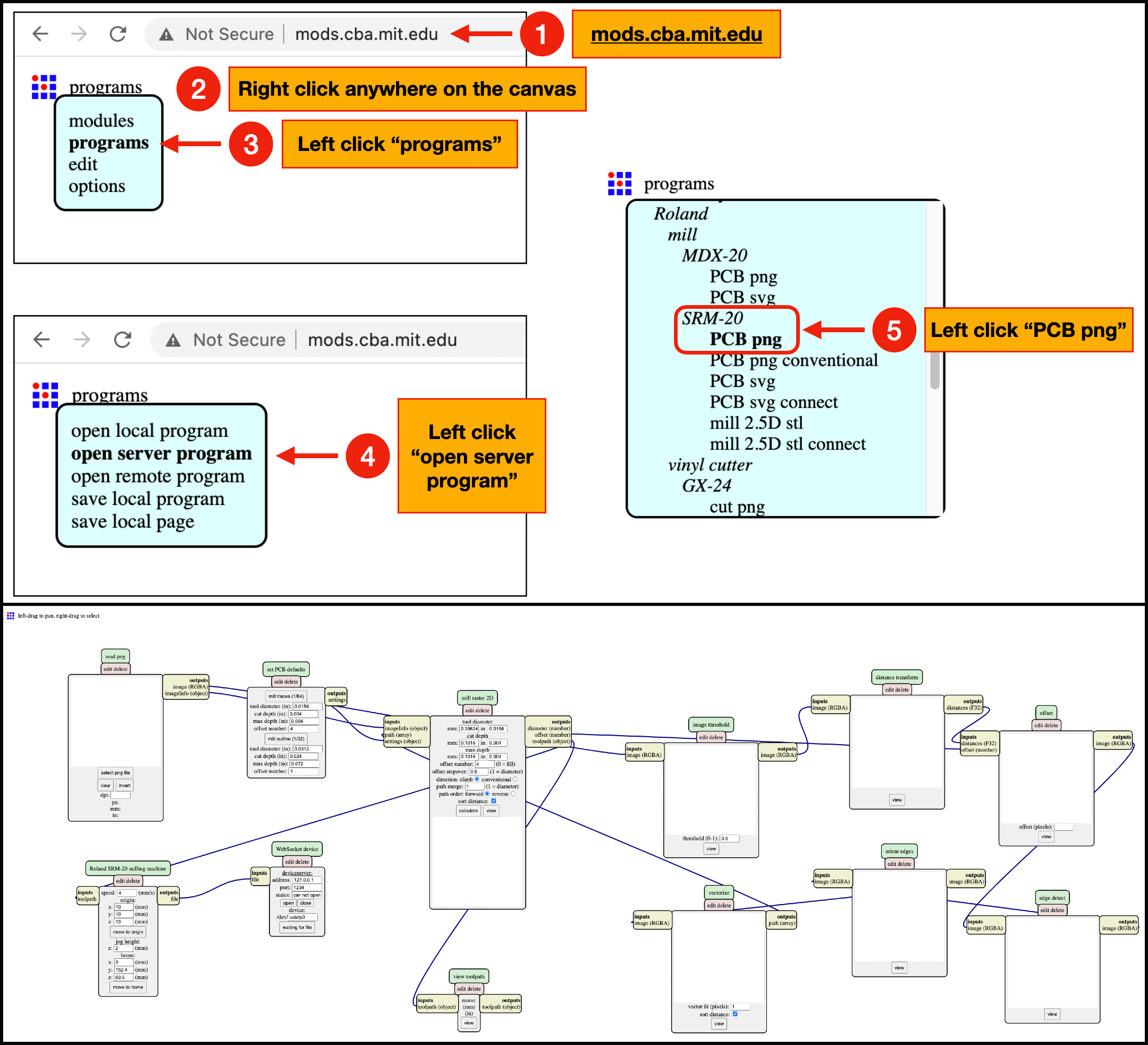
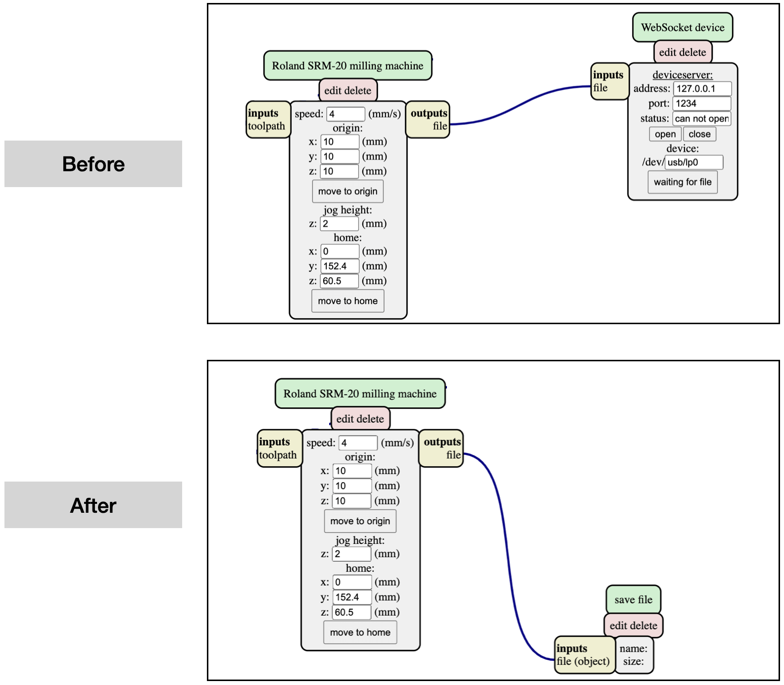
As we were not using internet connection, I deleted the WebSocket module and replaced with a file save module (module > open server module > file save). This workflow would allow automatic save after calculating the image.
I set my origin as (0,0,0). The default offset setting is 4 for the traces, and 1 for the outline. Here are the workflow that I followed to auto-save the G-codes (.rml) for the trace file and the interior file.
Setting Up and Milling the Precision Test
The PCB milling machine at the lab is the Roland SRM-20 desktop milling machine, and its bundle software is VPanel.

In order to understand how PCB milling machines work, I consulted former students' documentations, and I found Charlotte Latin School's group assignment page helpful for understanding the basic concepts:
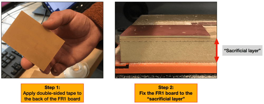
Next, I applied double-sided tape to stick the back side of the FR1 board to the "sacrifical layer", which was also secured on the machine base plate. During the review session, our instructors have reminded us not to overlap the double-sided tape because even a slight unevenenss can cause a major error during the milling process.
The circuit board material that we use is the FR1 Copper Clad, it is basically a sheet of a layer of copper covered on top of a material which is called FR1. FR stands for "fire retardant", and FR1 is the least toxic but also the least fire retardant. Standard circuit board material is FR4, which is made of glass fibers. Milling that is much more hazardous for people and for our tools.
In order to protect the tool, we should not place the FR1 board directly on the machine base (i.e. the aluminum profile); instead, we apply a double-sided tape on the back of the FR1 board and stick it to the sacricial layer (i.e. MDF board, acryic, or another FR1 board), which is glued or clamped to the machine base.
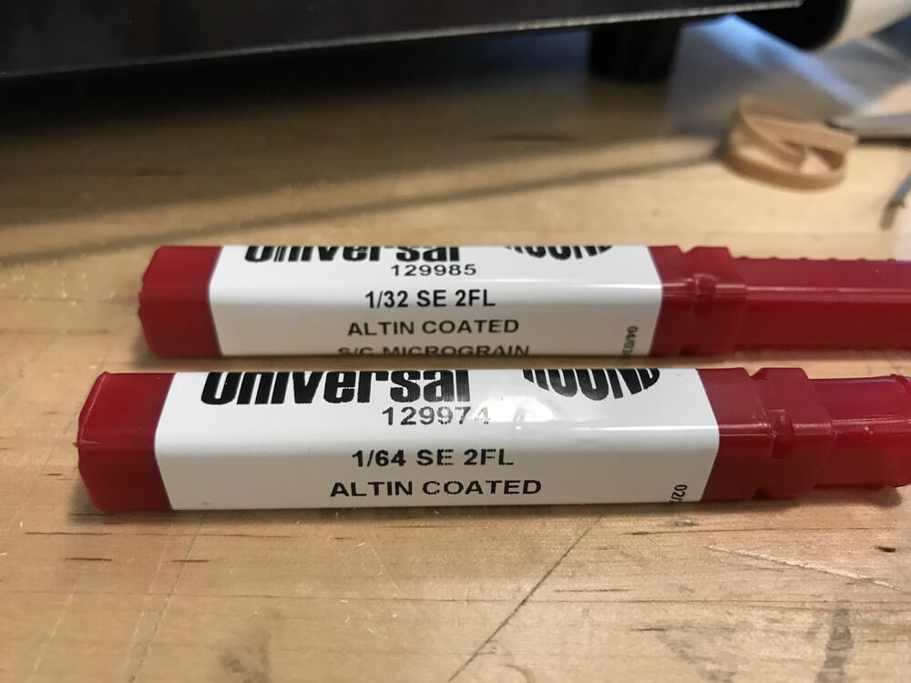
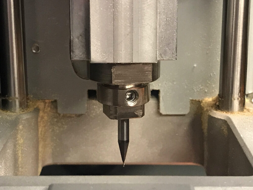
Next, I installed the 1/64" bit for milling the traces.
In order not to break the bit, we should exchange / install the milling bit by holding the bit with one hand and untighten the spindle holder gently with an hex key ("allen key") on the other hand.
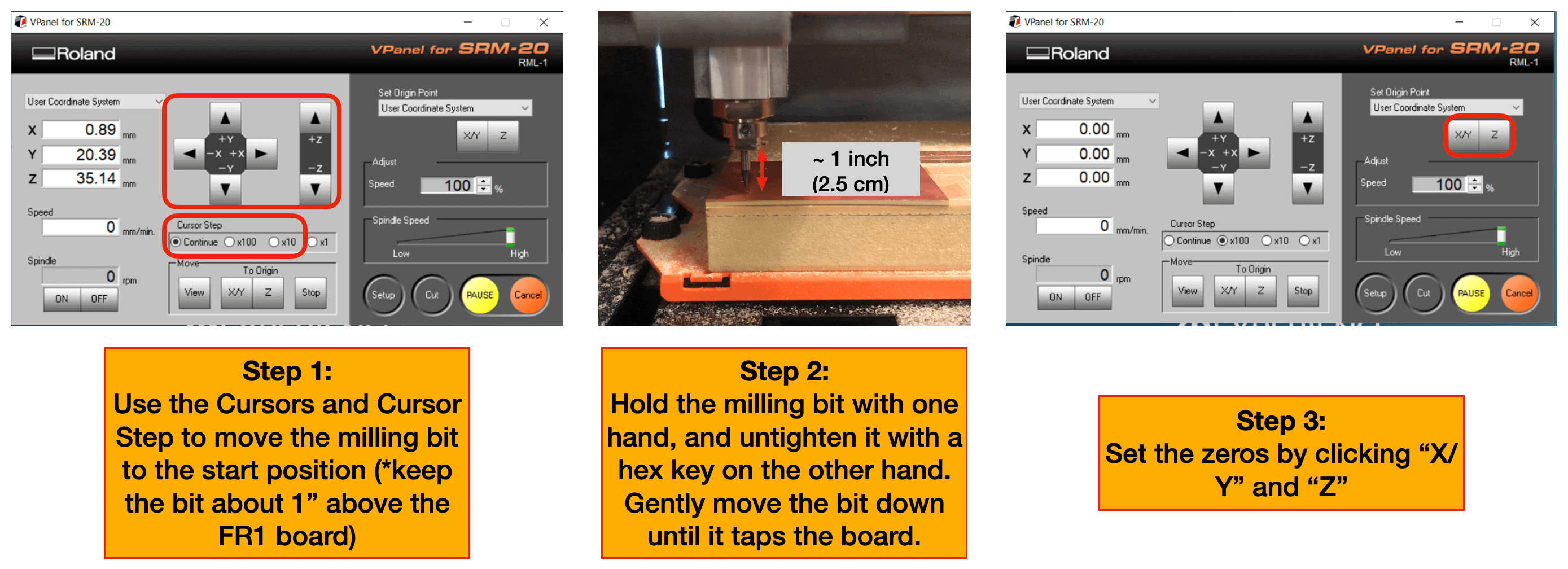
Next, I opened VPanel and set to use the User Coordinate System. I also set the origin point and z-align the milling bit by following the workflow below.
We learned through trial-and-error the importance of properly z-align ing the milling bit. After some exploration, we found that pushing the bit about 1 inch (~ 2.5 cm) down allowed for crisp looking traces.
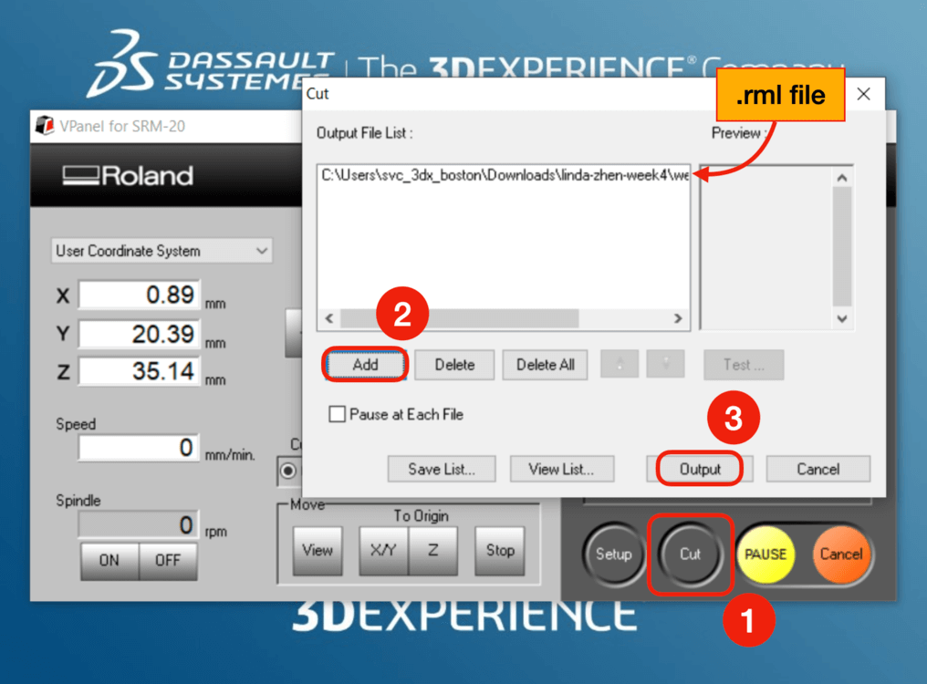
After setting up, I was ready to mill the precision test file. To begin, I imported the .rml file for the traces and clicked "output" to start the milling process.
Here is a short video of the milling process:
When that was completed, I clicked "View" on VPanel to allow the spindle holder raise as well as to paused the machine. I vacuumed the flakes and visaully inspected the traces.
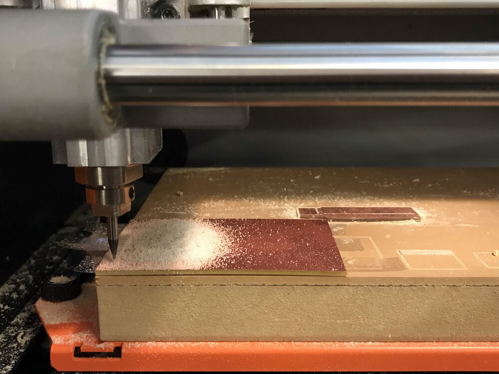
As the traces looked good, I then changed the bit to 1/32", and repeated the previous steps to set the origin, z-aligned the bit, imported the "interior" .rml file and continued the milling process.
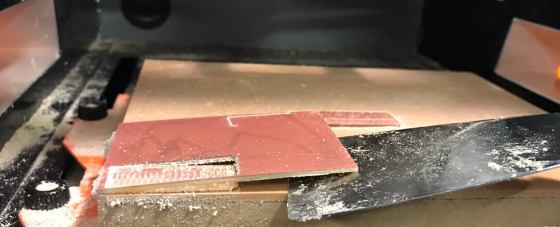
Once done, I vacuumed out the flakes and took out the cut part with a spatula.
Evaluation
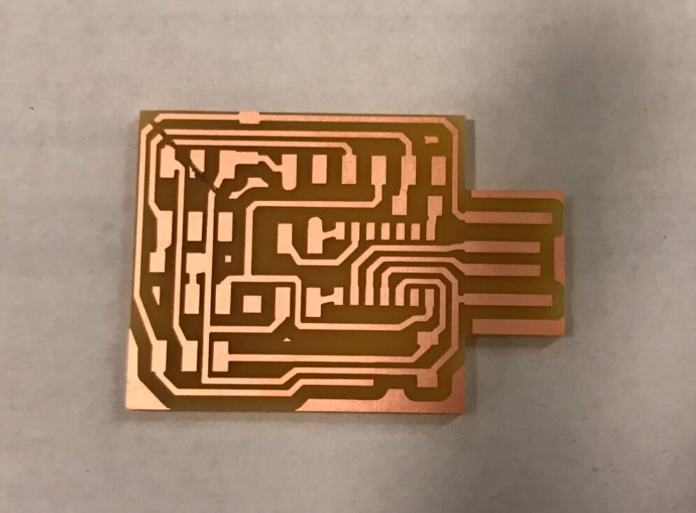
Here is the result of the precision test:
- The thin lines on the precision test help determine the largest offset we can use for milling PCBs. As shown from my precision test, the thinnest trace of copper has width of 0.001"; although the profile is still visible, a small section of the copper on the bootom of 0.001" - 0.004" were removed by the milling machine.
- The thinnes trace that has "groove" show on the top has width of 0.016", which is 1/64", the diameter of the milling bit that I used for carving the traces.
- I also noticed I was not setting the zero for the outline ("Interior") at the same location as the traces, and thus resulted in misalignment in the board. To rectify this issue, I should have just raised the bit in +Z direction instead of clicking the "view" button before changing the 1/64" bit to the 1/32" bit.
Individual Assignment: Making the In-Circuit Programmer
Introduction
Our instructors recommeneded us to mill SAMD11C14 board, which is a JTAG. JTAG stands for Joint (European) Test Access Group, and is designed largely for checking faults in chips/boards, I think. Neil and Spencer introduced us a little about ISP and UPDI, and I needed to look up for information and add it here.
Generating the G-Code Files
According to our local guru Luciano, the offset number determines how much separation our components will have. A larger offset means a greater separatation. Although having a larger offset will take longer to mill, it is easier to solder. As I wanted to set my offset for the traces file to 5, I measured the thickness of the FR1 board using a six-inch dial caliper, this would allow me to determine the cut depth. Here is a rough calculation to set the cut depth if I want to carve the traces in 5 passes:
- Tool diameter = 0.4 mm;
- Cut depth = maximum depth = thickness of the copper layer on the board = 0.4 mm;
- Since the offset = 5, we will need to set the cut depth = 0.08 mm so that the same process will pass through the material 5 times to reach 0.4 mm.
I also wanted to lower the feed rate (speed), so I set 1.5 mm/s for the 1/64" milling bit, and 2 mm/s for the 1/32" milling bit. The images below show the workflow that I followed to realize the G-codes for the "traces" and "interior" files of the SAMD11C board.
Milling the SAMD11C14 Board
I followed the same process as the group assignment to set up the machine and milled the PCB. Learned from the previous experience, I didn't click the View button from VPanel after finish milling the traces. Instead, I raised the 1/64" milling bit in the +Z direction using the cursor panel, and changed the bit to a 1/32" bit to mill the outside profile. I made this change to ensure the traces and the interior align perfectly in the final result.
Here is a trimmed video of the milling process:
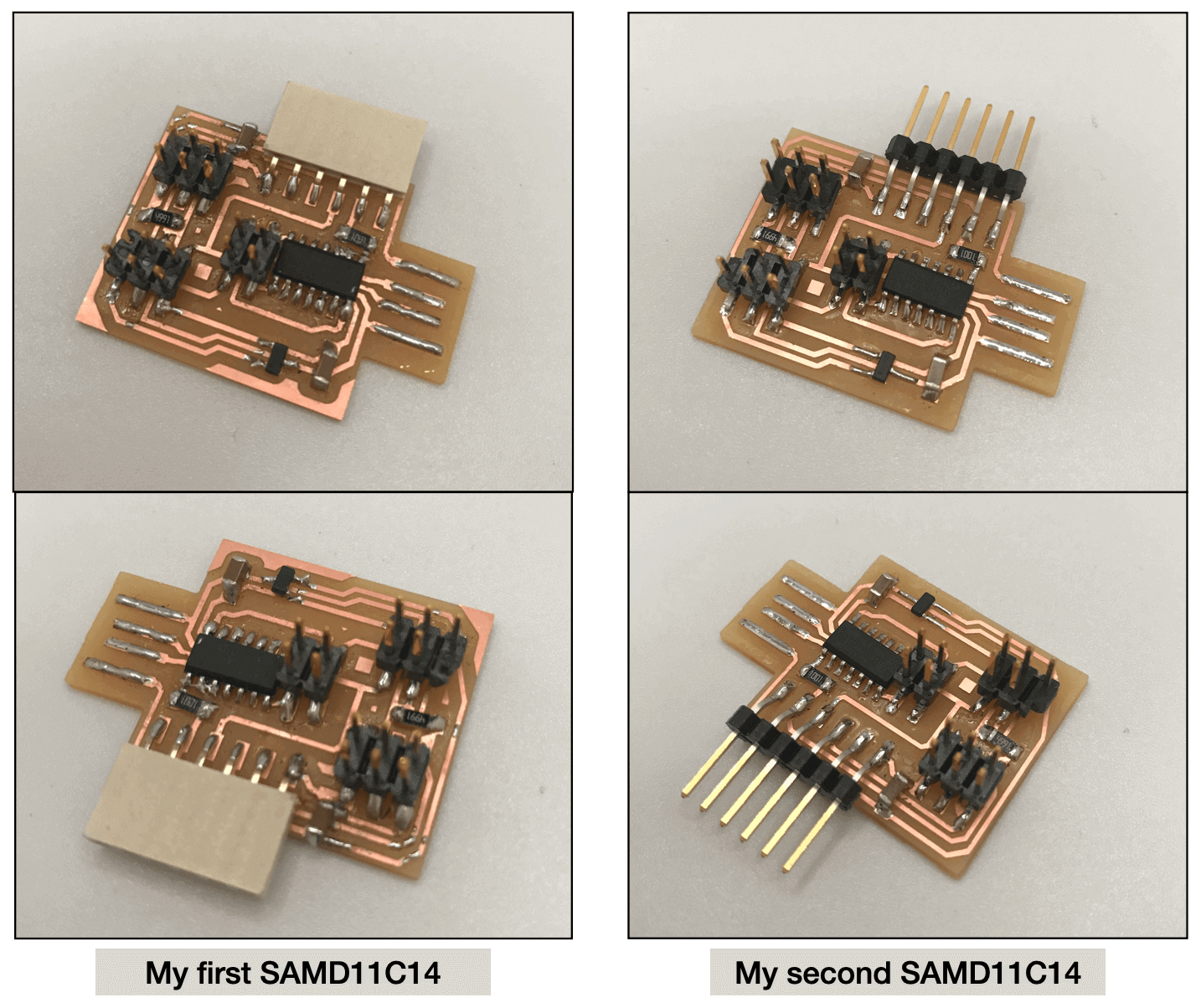
The total milling process took about 35 min, however I counted this as a high turn-around time for milling such a high-precision board. When all is done, I inspected the board and I noticed a few copper traces on the top left corner were scratched through 😱. My instructor and I were concerned about disconnection, but we thought that probably this could be rescued by soldering thin lines of tin on those broken traces, so the next step for me was to start the soldering station as I had collected my components for my board (more on this on the next section). Before that, I had set up the PCB milling machine to mill another board as a back-up. I told myself, the worst case would be this board not working but I would still able to build my soldering skills, and I would not have to wait for 35 min to get a new board on another day... so I felt relieved again 😄!
Here is an image of my PCB after being post-processed with soap and water and dried.Before soldering, I scrapped off some copper along the outer side of the USB to prevent it from possible short-circuiting
.
Stuffing the PCB
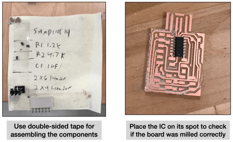
After degreasing my board and drying it really well, I was ready to solder my first PCB. I borrowed my instructor's method for collecting the components with a double-sided tape and making sure the board was correct by placing the IC component on its position to check if the legs all positioned on its right spot.
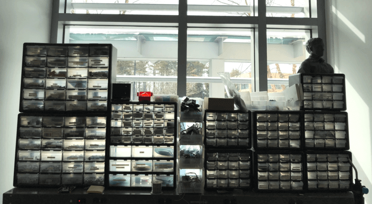
There was a wall of drawers for the electronics components at the lab, when gathering the components, I took one component at a time from the little drawer and placed it back before taking another drawer with the next component(s).
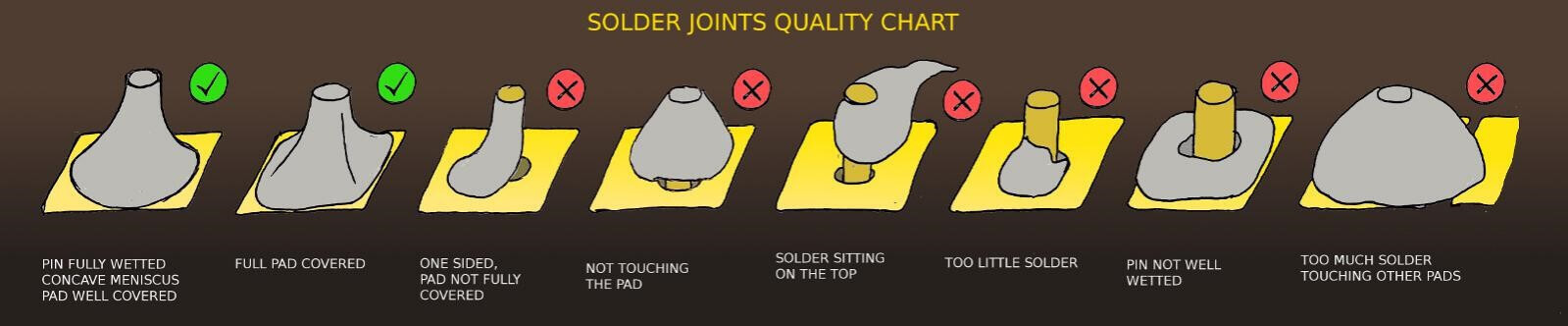
Over the weekend, I reviewed Duaa's soldering lecture during the student bootcamp as it was packed with useful tips for soldering. Particulary, I found this image helpful for determining the quality of the solder joints.
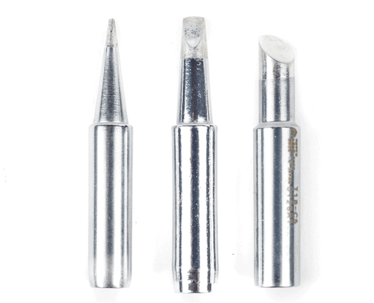
I also found the following image helpful for selecting the right soldering iron to solder SMD components (Surface Mount Devices). The soldering iron at the lab was the Weller WES51 soldering iron, it has a very fine tip and was of great assistance to a starter like me.
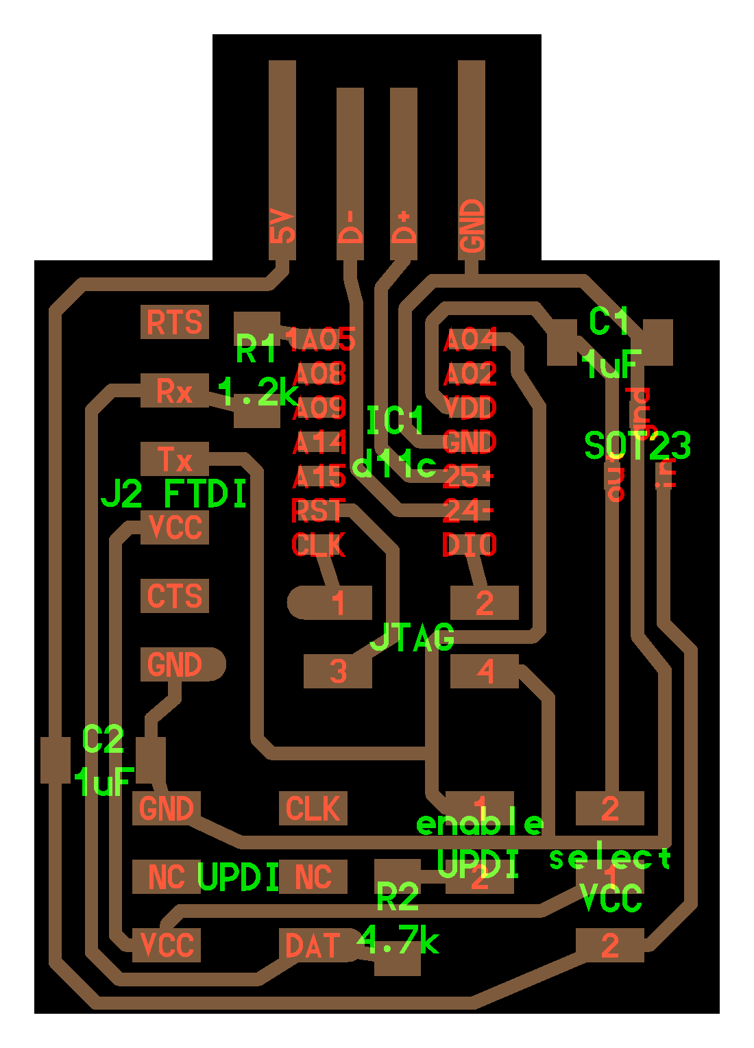
The rule of soldering the components is as follows: "center to out, small to big, low to high, difficult to easy". To me, my order of soldering for this board was as follows: first the the microcontroller, since it sat at the center of the board and had the smallest legs; then the n-Channel MOSFET, followed by the resistors and capacitors, and lastly, the headers. While soldering, I also referred to the schematic and board image of the board.
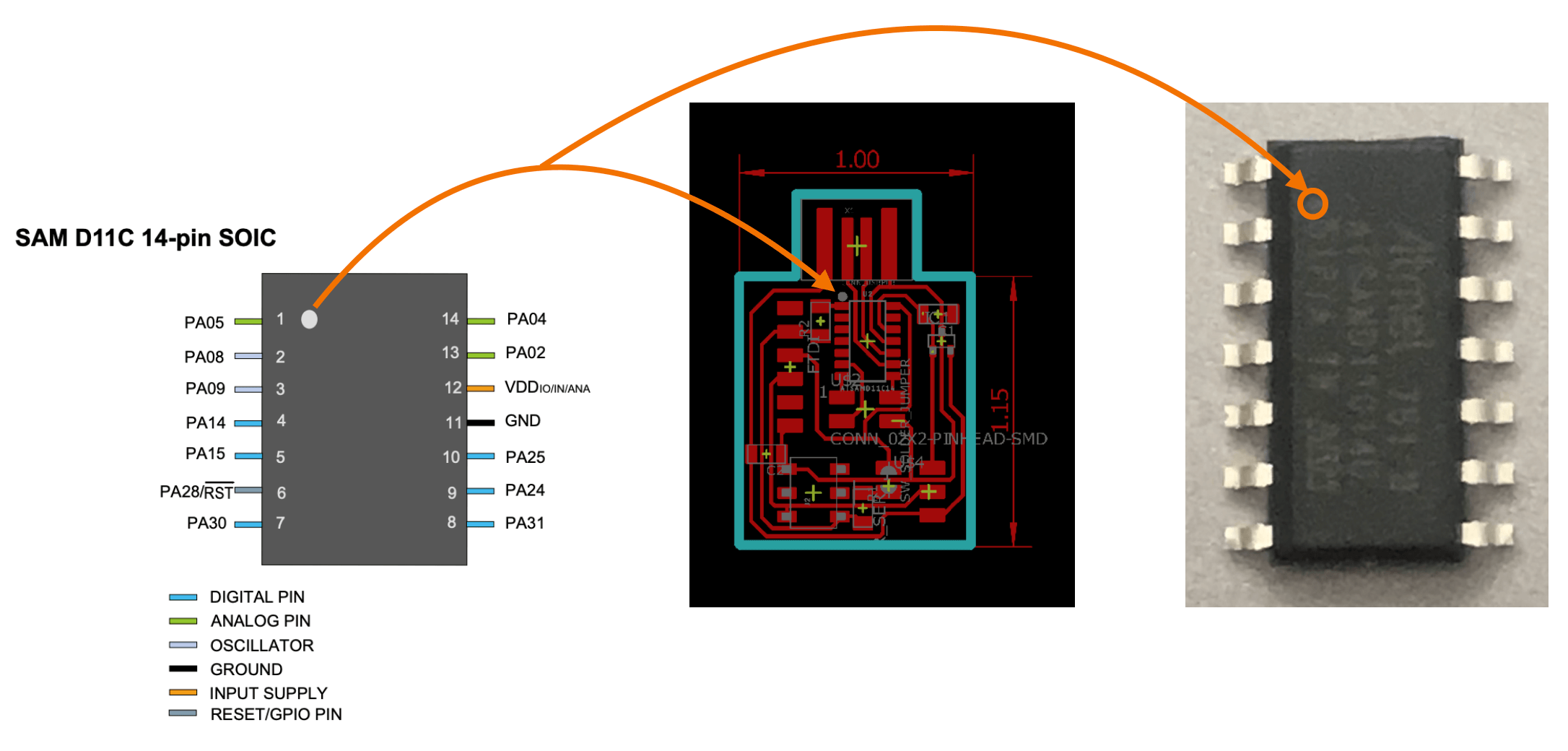
Another thing that I also needed to be careful of was to make sure the microcontroller was placing in the right orientation. As shown from the image below, there was a white dot at a side of the component indicating the polarity. To solder the SAMD11C14, I first added a little solder to the left-top trace to fix the chip in place, then did the same thing to the leg that was facing diagonally to it, then finished off the other legs using the rule of soldering from above. The process was not as easy as said as I had very shaky hands, eventually, I got more comfortable with the process and started to pick up the pace.
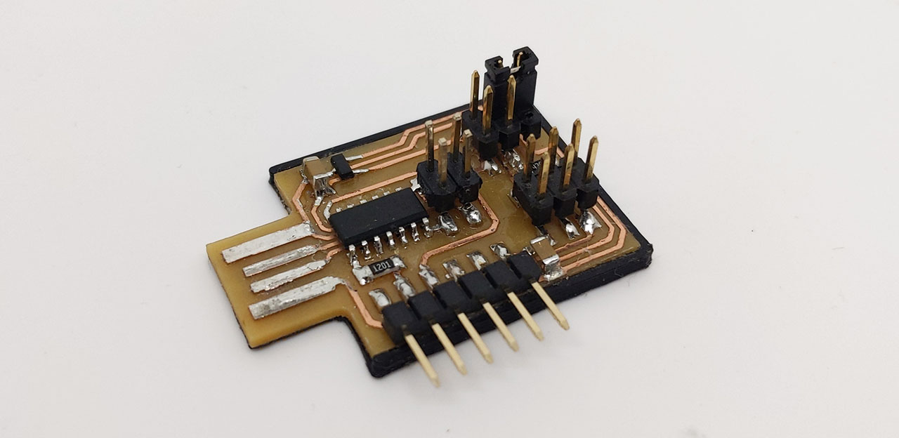
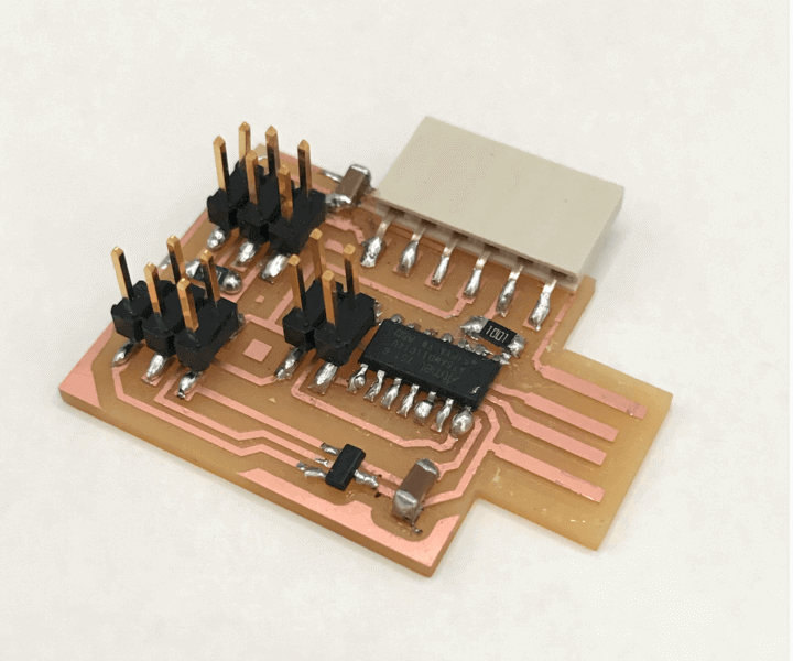
Here is a "hero shot" of my first soldered PCB. As mentioned above, I had to solder thin lines of tin on some broken traces hoping to make it work, at this point, I still didn't know the answer, but I was hoping for the best.
Testing and Debugging the Board
Mar 8, 2021During the Electronics Design week, I finished soldering my second SAMD11C14 because the one that I did on Week 4 didn't pass the continuity test due to broken copper traces in multiple places. Once again, I used Quentin's board image as the reference when soldering my board, and tested with a multimeter to make sure everything was connected where it was supposed to be and not connected anywhere else. This time, I learned to be patient and heated my solder for a little longer before letting go of the soldering tip. I was pleasantly surprised by the result from using this trick and also my improvements within these two weeks.
FTDI Programmer: Milling, Soldering, and Programming
Jun 20, 2021As I have not been able to program my SAMD11C14 board on my Mac using the JTAG programmer, I chose to work on an FTDI programmer to fulfill the last part of the assignment for now. I would still like to revisit the EDBG programming on my SAMD11C14 post-fabacademy!
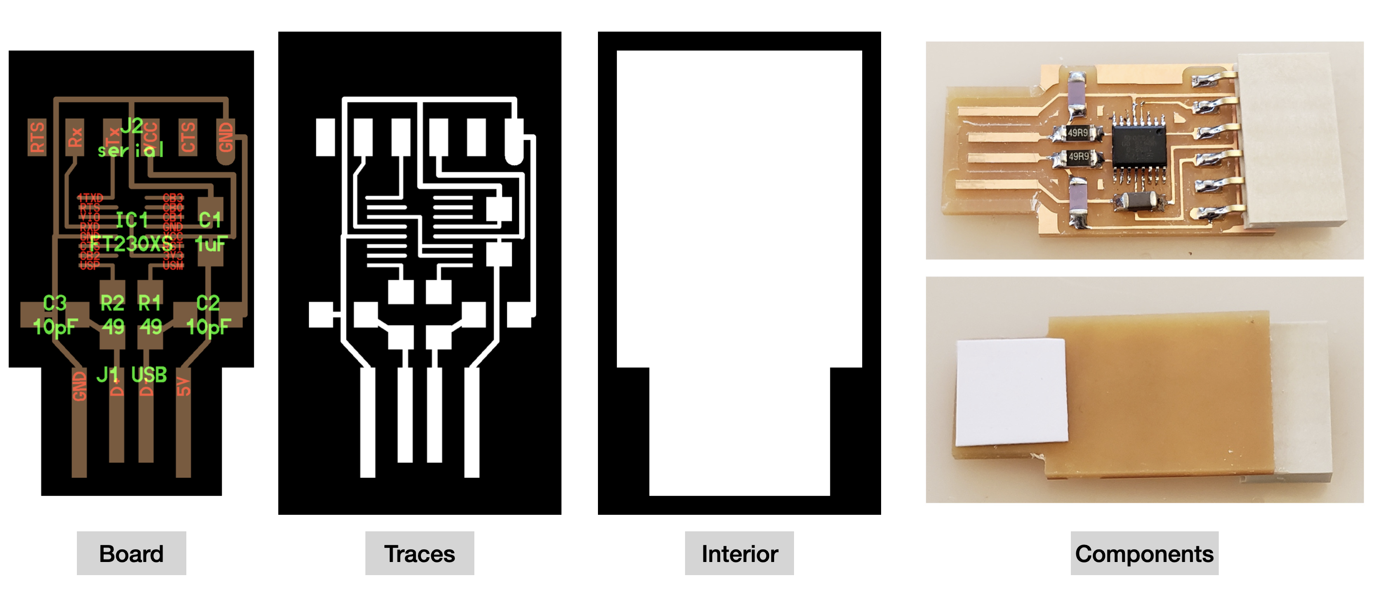
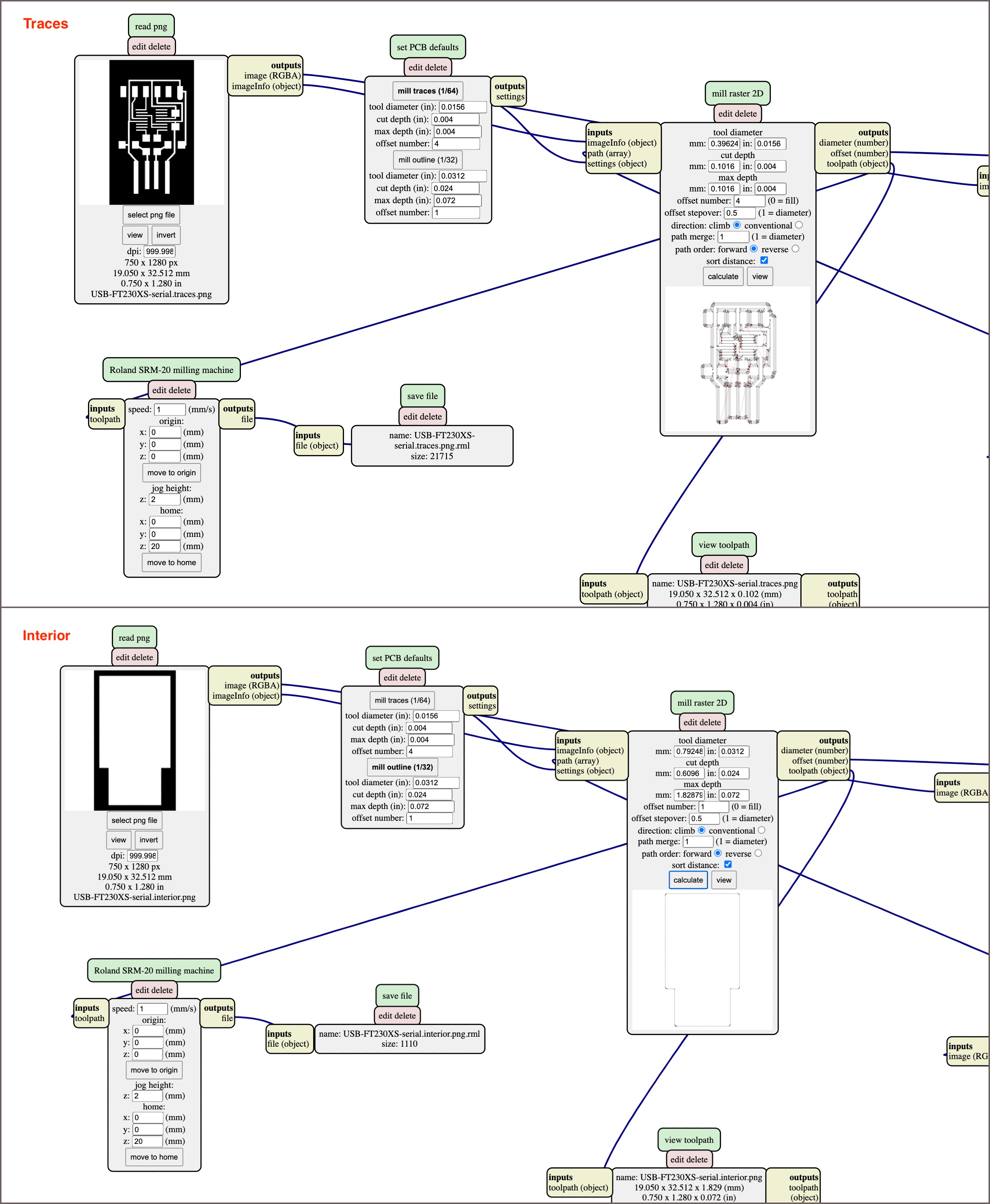
I downloaded the traces.png and the interior.png files of the board, and generated the .rml files (G-codes) for milling. The milling machine that I set to use was Roland SRM-20 at the lab, thus in mods, I chose the folowing program: Roland SRM-20 / PCB png. The majority of the G-code generation process was the same as the SAMD11C14 board, however, since the traces of the FT230XS was very fragile, I needed to handle with care. I set the cutting speed as 1 mm/s (default is 4 mm/s) for both the traces and interior. Here is a snapshot of the G-code generation process.
I used the 1/64" milling bit for milling the traces, and the 1/32" milling bit for the inteior. The milling process was smooth and the result was beautiful to me. Once I removed the board from the machine, I used an FT230XS chip to make sure the scale was correct.
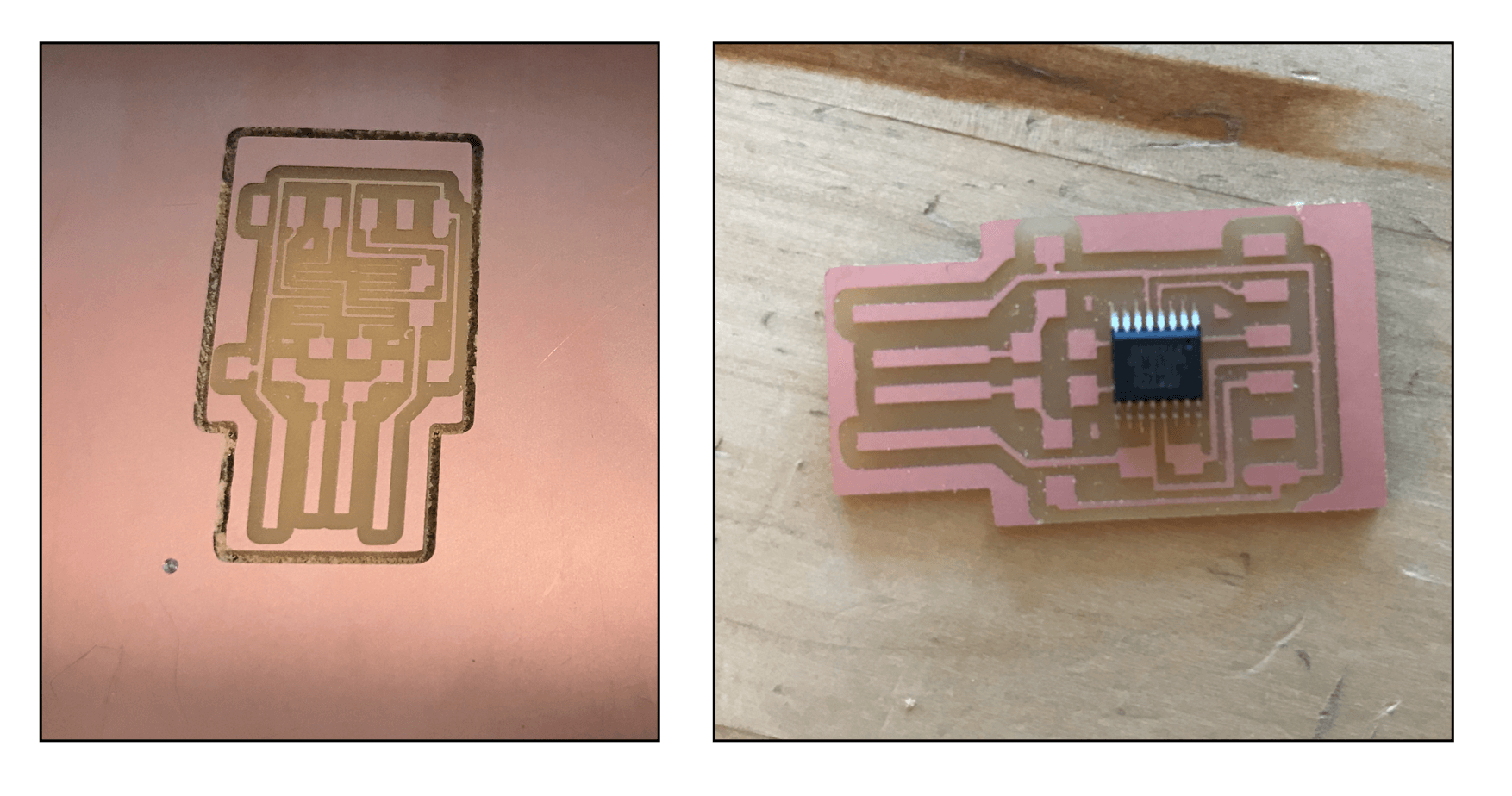
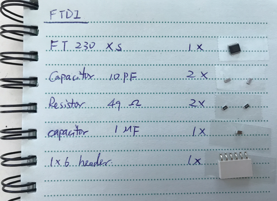
I removed the excess copper in front of the USB traces, I then cleaned the board with water and soap to remove any excess copper debris in between the traces. After that, I prepared the list of components and was ready to solder:
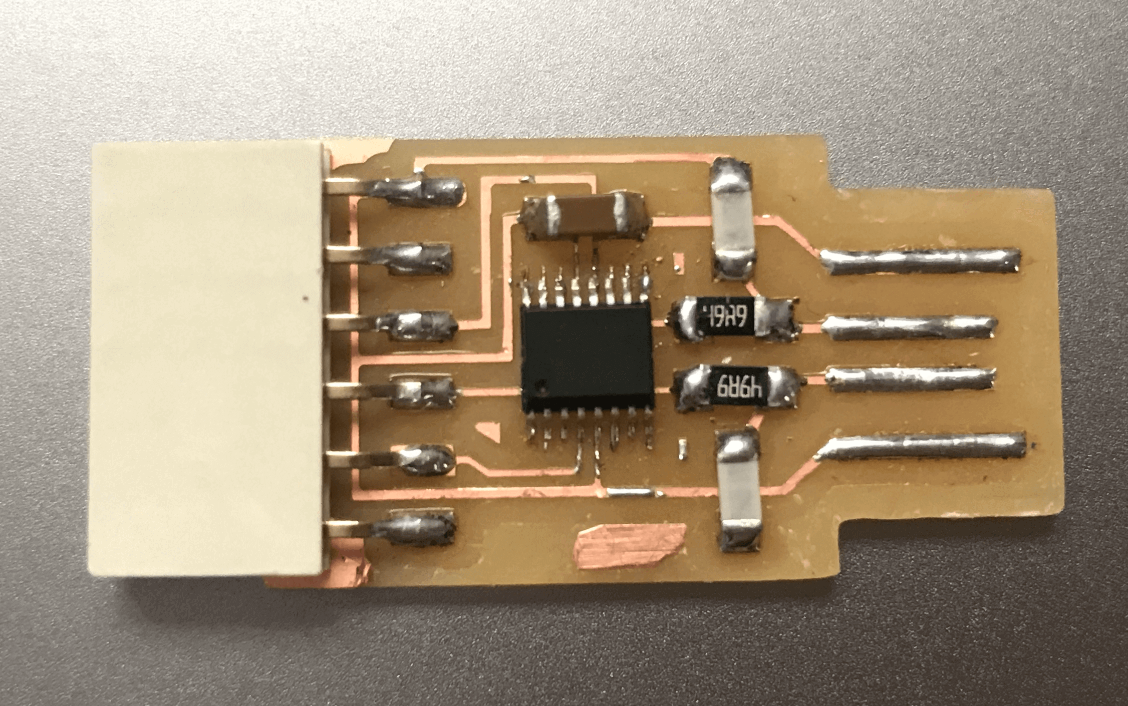
As the traces for the FTDI were very thin, I had to several attempts to get the soldering right. I made sure the orientation of the FT23OXS chip was correct. During the process, I used the multimeter to check for continuity. I tinned the USB-PCB to help with connection in the later step. Here is the end result of the soldered board.
As the FT230XS chip didn't require any pre-programming, I only needed to make sure my computer recognize the chip. I plugged the board to my USB hub, but it was not recognizable. I referred to FabLab Kamakura's documentation and learned that the problem could be from the USB-PCB. I double-checked the continuity and confirmed that the components were connected correctly, so I tried the second method, by taping a layer of electrical tape on the back of the board, however the board was still not recognizable. At last, I changed to a new USB hub and this time it worked!
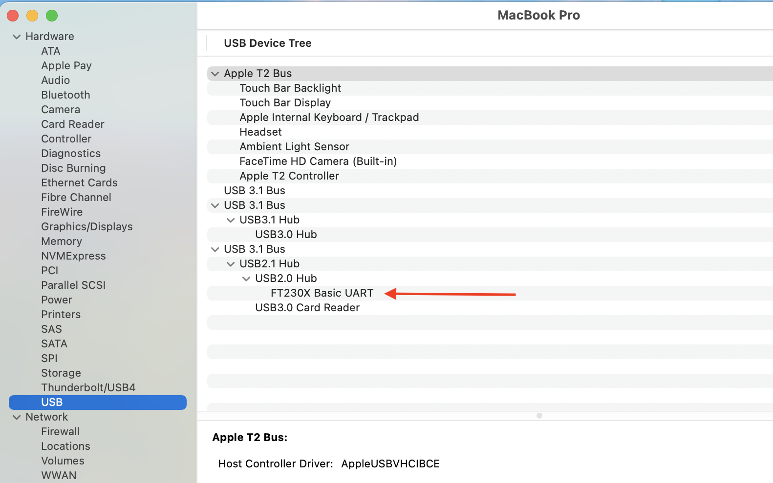
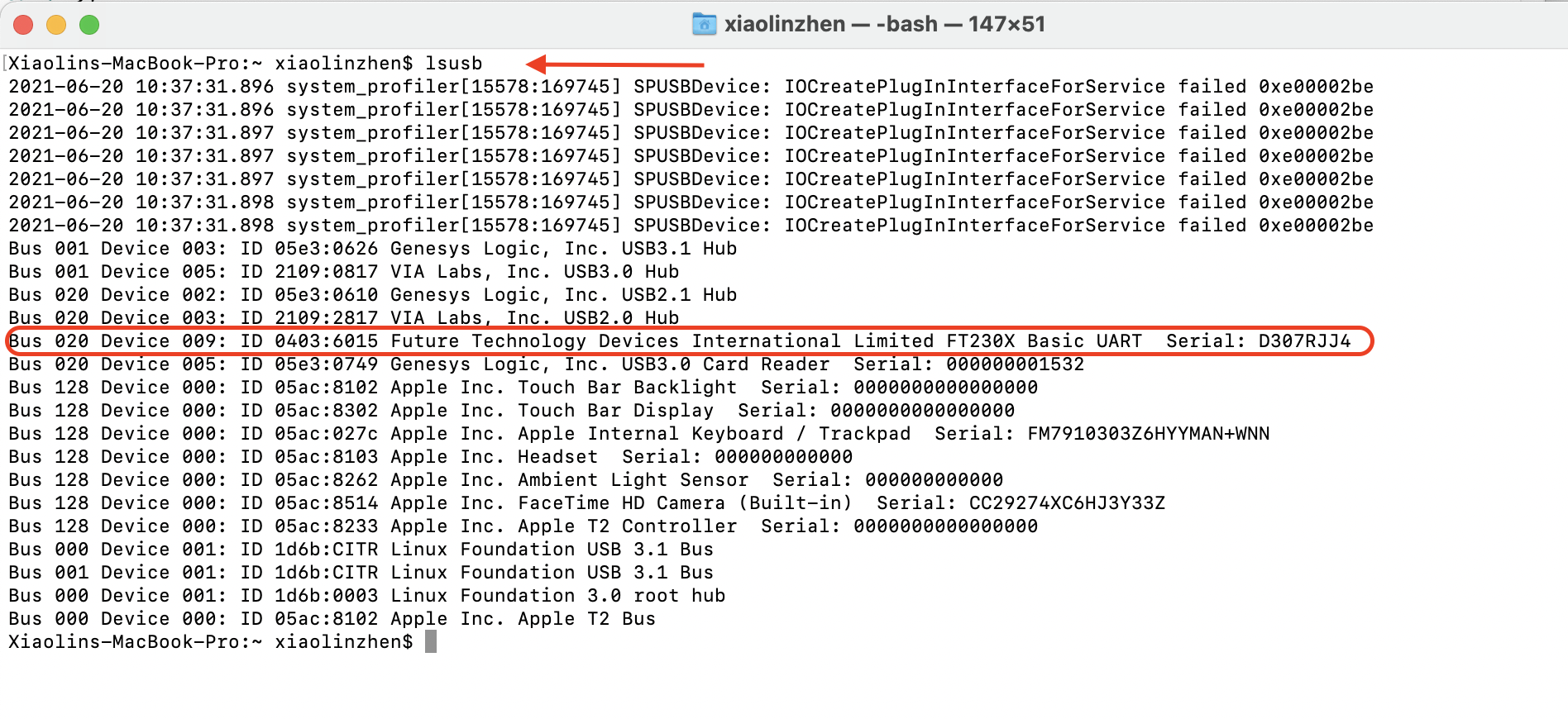
I had brew install lsusb on my computer, and got another confirmation that the FTDI programmer was recognizable this time.
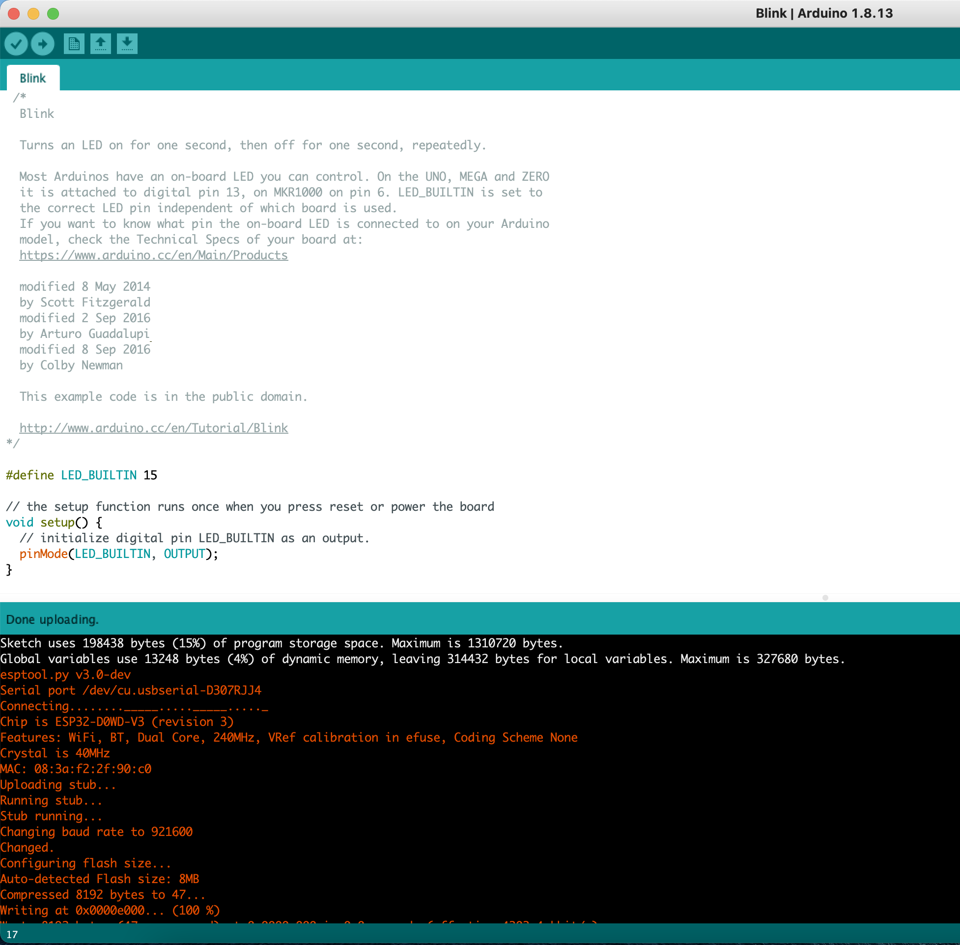
Next, I proceeded the programming part of the assignment. I connected the FTDI directly to my ESP32 FR1 board. In Arduino IDE, I opened a blink LED example sketch:
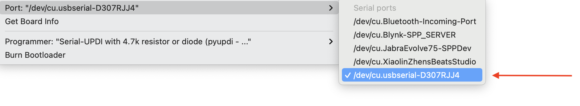
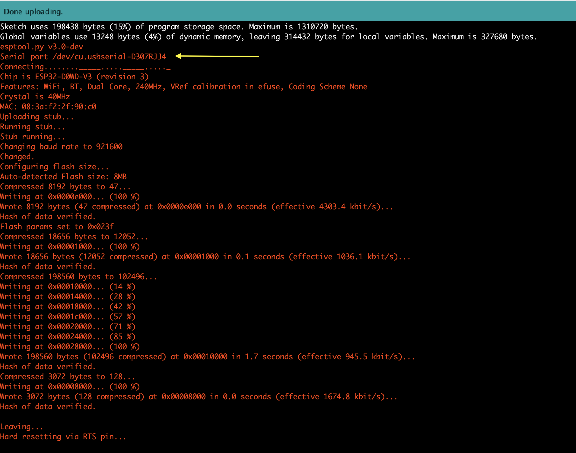
And selected the board, programmer, and port. As shown in the image below, the Serial Port for my programmer was D307RJJ4 , which was confirmed by lsusb above.
After I knew that the serial port was correct, I proceeded to upload the sketch. Here is a snapshot showing successful upload.
I clicked the Reset button on my ESP32 board, and the LED started blinking. Here is a short video showing the result. Yay it worked!
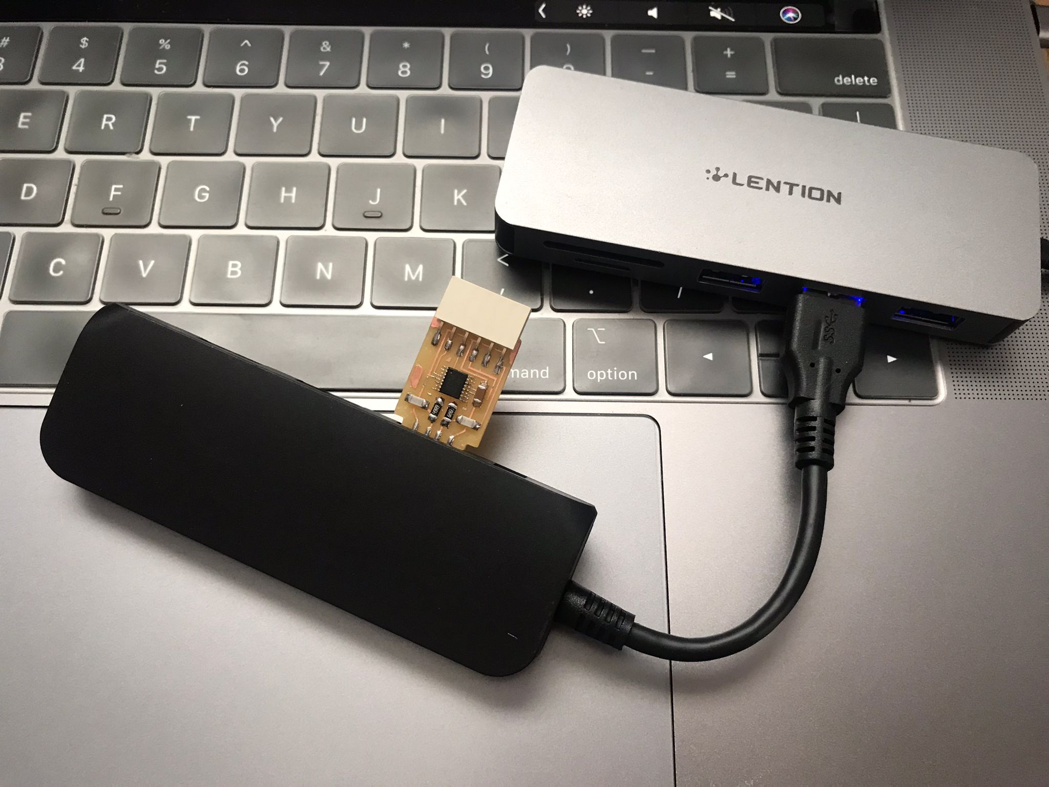
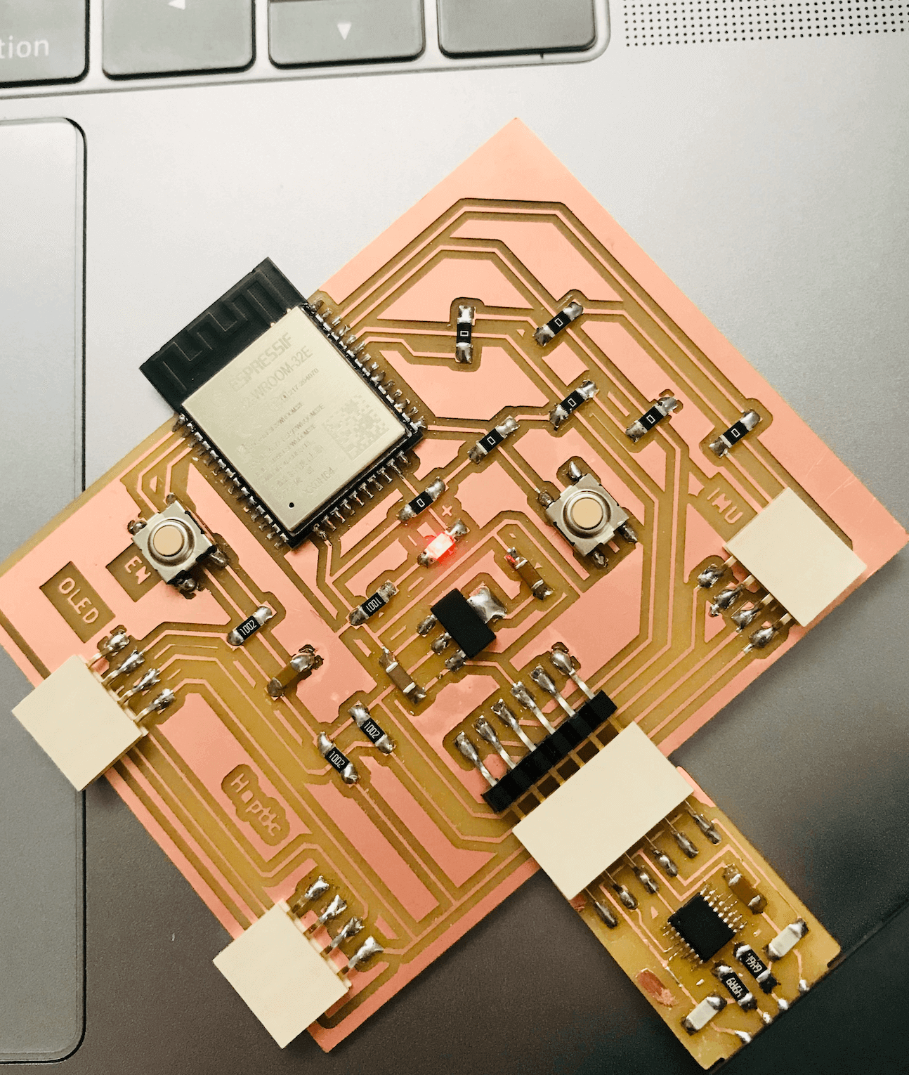
Here is a hero shot of the two boards:
Files
Please find below the files that I made for this assignment.
- Group Assignment - Precision Test
- Individual Assignment - SAMD11C14
- Individual Assignment - FT230XS FTDI Programmer