Electronics Production
For this week's assignment, the purpose was to reproduce a Printed Circuit Board (PCB) using the milling technique. The goal was to mill the board by preparing the G-Code file and then solder the components. At the end we had to program the board using the terminal. For the group assignment we had to characterize the design rules for the PCB production process.
Printed Circuit Board
A Printed Circuit Board (PCB) is a board made for connecting electronic components together. It is made by combining different sheets of non-conductive material, such as fiberglass or plastic, that easily holds copper circuitry. The electronic components are soldered onto the PCB where appropriate. PCB is also known as printed wiring board (PWB) or etched wiring board (EWB). PCB's are found in nearly every electronic and computing device, including motherboards, network cards and graphics cards to internal circuitry found in hard/CD-ROM drives. There are different techniques that can be used to create a PCB. For example etching, sewing and miling. Furthermore there are also various materials that can be used to produce a PCB such as FR2, FR4, aluminium, paper or cardboard and even different kinds of textiles.
Fab Modules
As we have to reproduce an existing electronic design, we only have to prepare the file for the CNC machine. To do that I used the Fab Modules software. This software is used to run any fab lab machine.
I am going to reproduce the circuit of the FabISP created by Andy Bardagjy. To create the milling traces for the CNC machine, I have to upload the PNG image on the Fab Modules software. Then you have to choose the machine you are going to use, to produce the correct G-Code file. Since I will be using the Roland Mill MDX-40, I select the Roland mill.
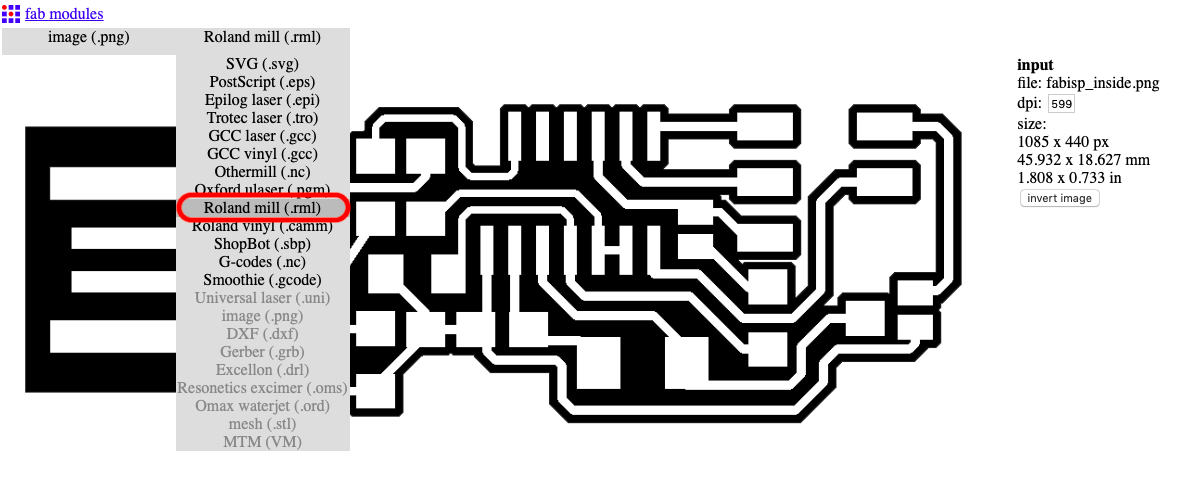
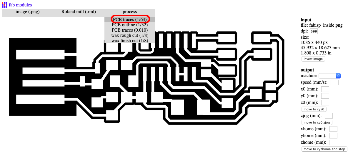
To mill the traces of a circuit board you will generally want to use PCB traces 1/64 as process. To understand the different processes I did some tests. The process PCB traces 1/64 is used to mill the traces and the PCB outline 1/32 is used to cut out the board.
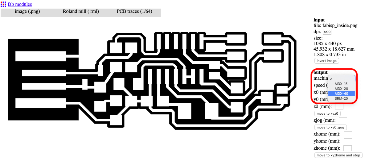
Moreover select the right version of the machine. Since it's a MDX-40 I am going to use, I choose it as a setting.
Every job has his own specific configurations. For my job I have set the following configurations to mill the traces:
After setting up the configurations, go to calculate. To make the software calculate the path for the milling process.

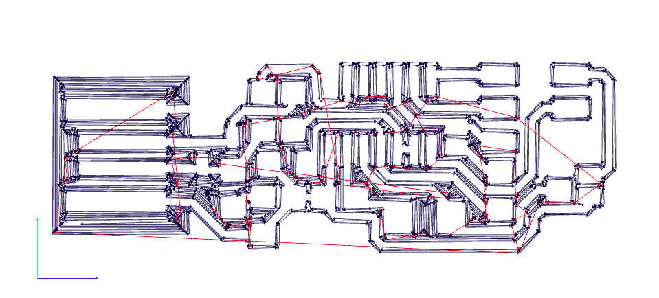
The image underneath shows the calculated version of the file. The blue lines represent the path that the tool is going to follow to remove the copper and create the circuit. The red lines display the travel directions. Here you can check, if everything is well-designed. Sometimes when you design it's hard to tell, if there is enough space between the traces. If there is not you will see it as soon as the software calculates the image. In this case everything looks good, so I am going to save the G-Code.
Next repeat the process to create the G-Code for the cut out. Change these settings:
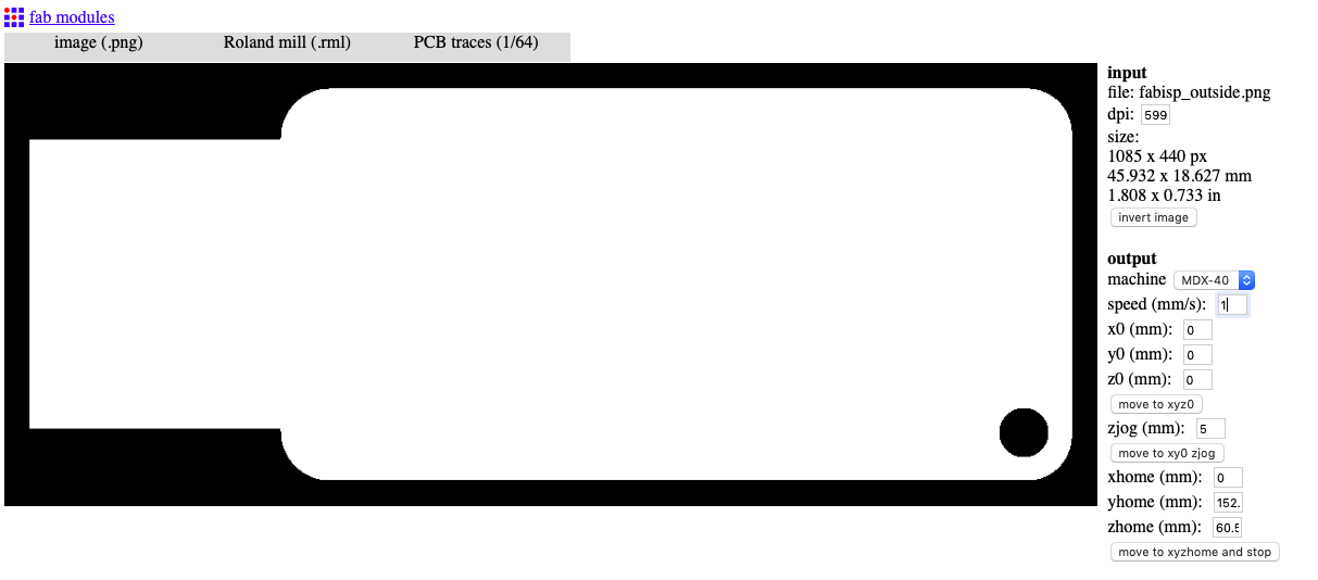
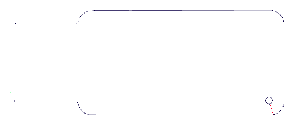
If you decide to use the PCB outline 1/32 process, there are some usefull facts that you should know. The 1/32 process has beside the cut depth setting another setting called stock tickness (mm). The stock tickness corresponds to the thickness of the board surface.
This means, that if the stock thickness is 1.7mm, but the cut depth is 1.9mm, the machine will only cut up to 1.7mm. You can see this in the generated G-Code file, that you develop for the machine.

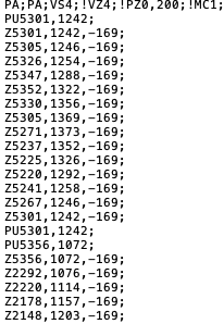
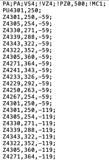
If you set a cut depth of 0.6mm and a stock thickness of 1.7mm, the machine will cut level by level. The first time it goes down to 0.6mm to cut out the outline of the board, then for the second time it goes again 0.6mm deep to mill the outline. It repeats this untill it reaches the stock thickness of 1.7mm. If you use these settings the job is going to take much longer, as the G-Code is three times longer then before. This process is similar to the 3D Printing. The cut depth acts here in the same way as the layer height setting of the 3D Printer.

CNC Machine
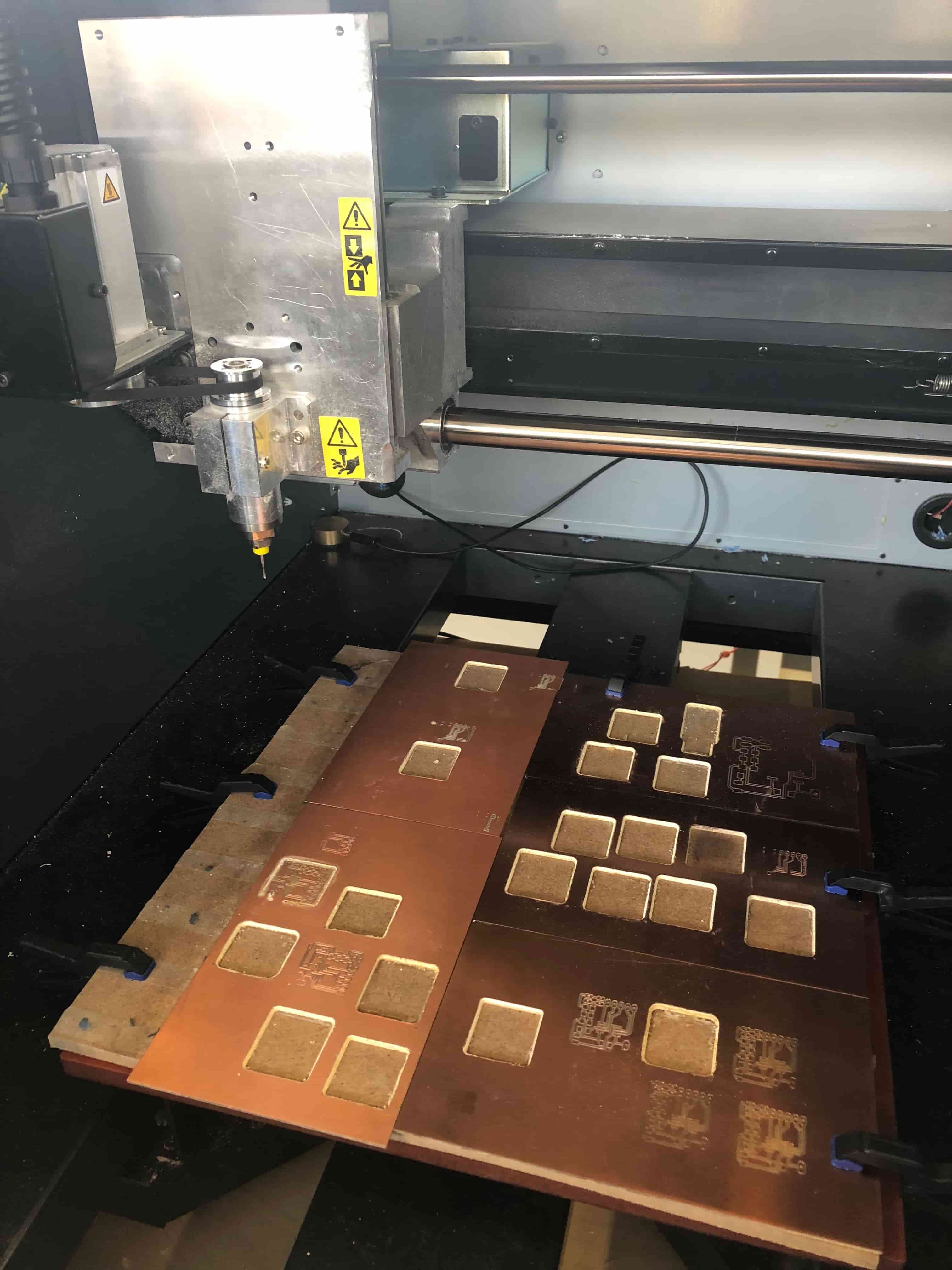
Below you can see the Roland Mill MDX-40 I used to complete the assignment. CNC milling is a specific form of computer numerical controlled machining. Milling is a process similar to both drilling and cutting. Like drilling, milling uses a rotating cylindrical cutting tool. The milling machine is able to move along multiple axes, such as the 3D printer. Most machines offer from 3 to 5 axes, providing performance along at least the X, Y and Z axes. Moreover almost any material can be used in a CNC machine. It really depends on the application. However, most CNC work with metal materials.
Group Assignment
You can find the documentaion of the group assignment here.
Using Roland Mill MDX-40
Before you start with the milling, it is very important that you attach the appropriate tool for the job. As I mentioned previously I used a 0,2 mm tool diameter to mill the traces and a 1 mm tool to cut out the board. Furthermore you have to make sure, that the copper surface ist fixed on top of the milling area, so that it won't move while the machine is operating. Also be certain that the plate is even, otherwise it may occur that not all the traces are going to be milled with same depth. Then start to move the tool to a place where you have enough space to mill the board. The most difficult part is to set the z axis, since the bit is very fragile. Next I am going to explain which method I used to set the proper height.
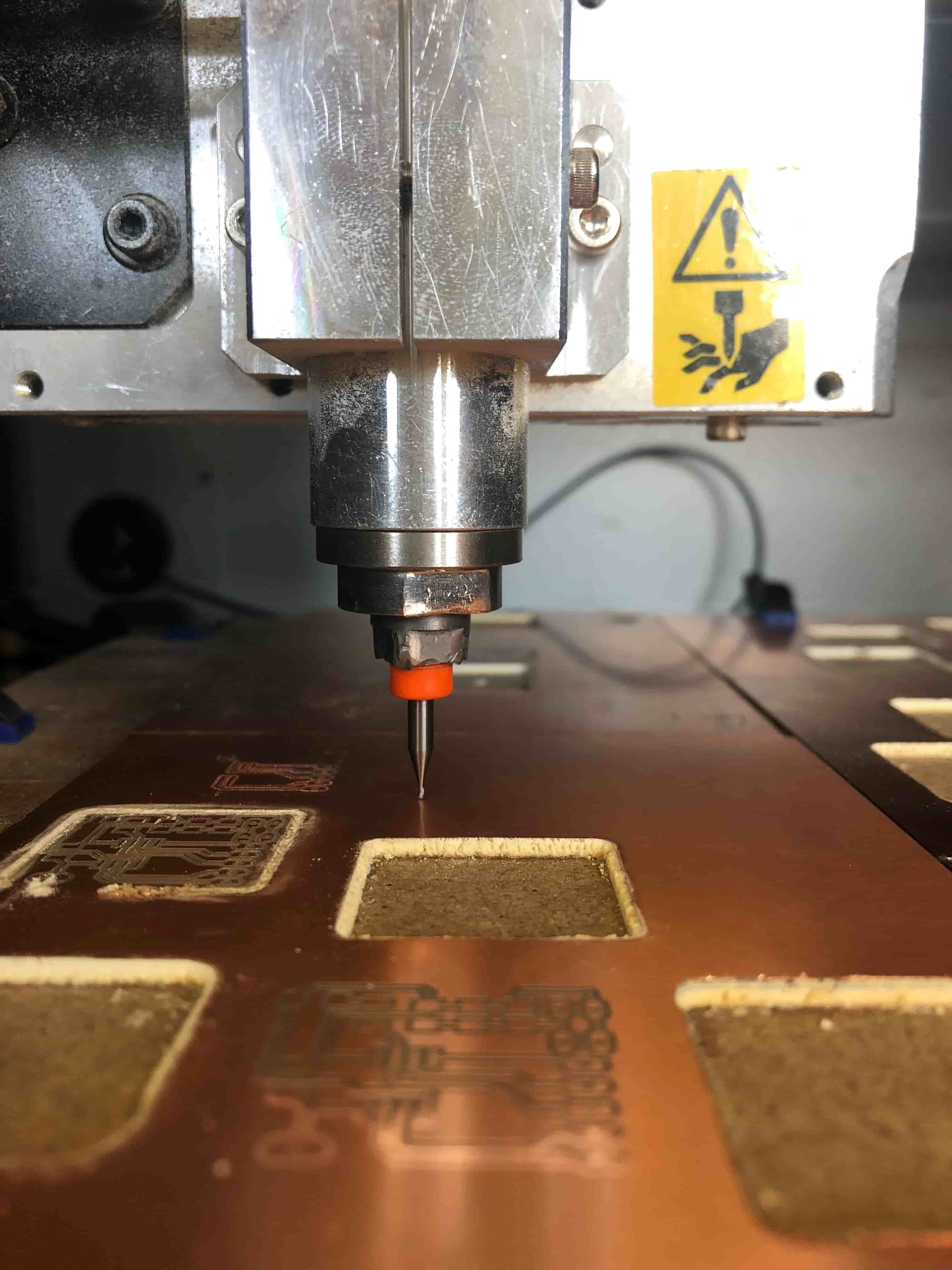
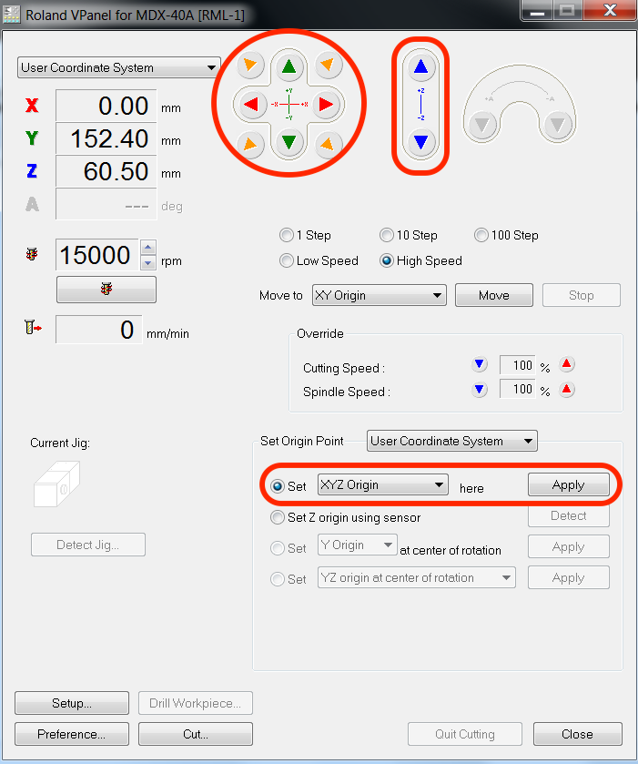
Underneath you can see the software that operates the machine. To move the machine in different directions use the arrows. In addition set the rotating speed of the bit to 15000 rpm. As I said before the bit is very fragile, so look after the speed you are using while moving the machine. To be sure that the tool is slightly touching the copper surface, I used a multimeter. Hereby I could recognize if there was a connection between the bit and the copper surface. Once there is a connection click on the apply button and set the new origin.
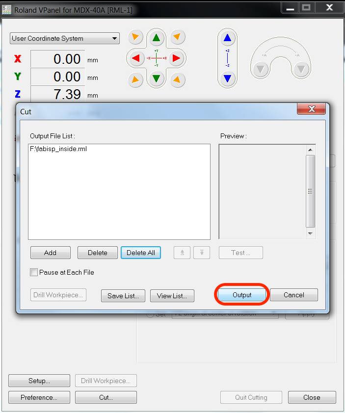
Next click on cut and delete all the current jobs that are shown in the output list. Then add a new job.
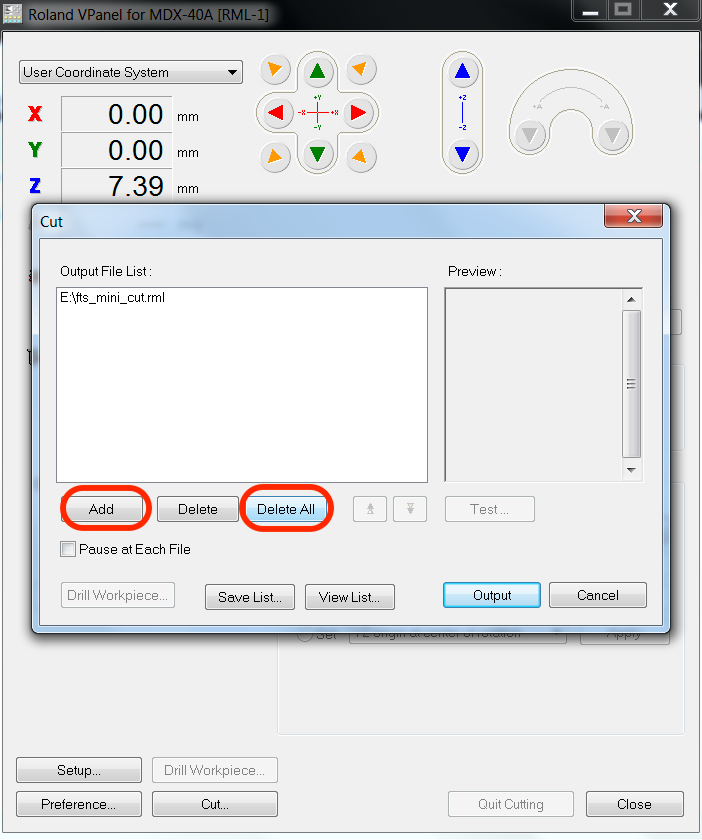
Now you only need to send the file to the machine.
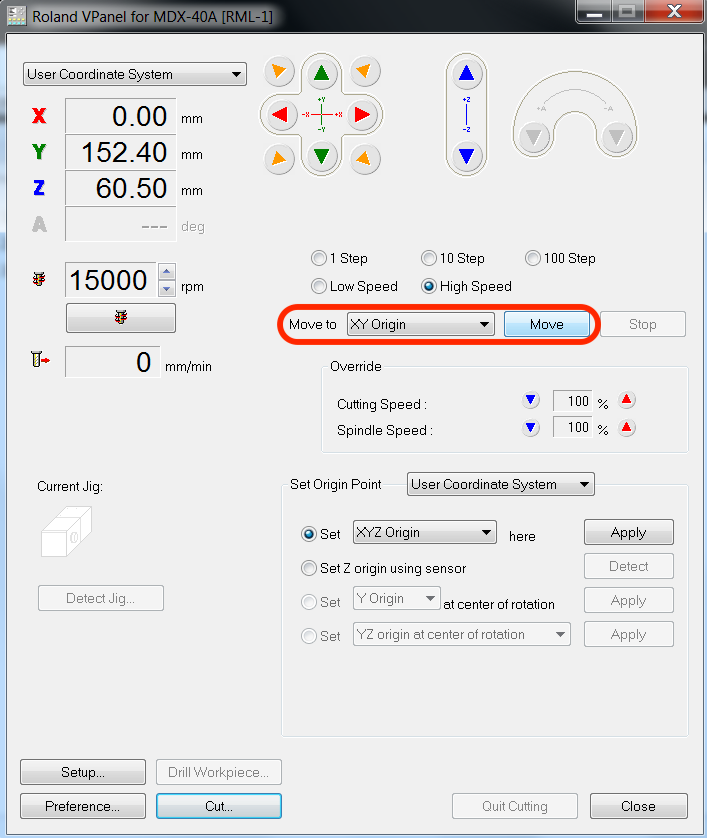
To cut out the board we first need to change the tool by using two wrenches. Then we can move the machine to the previous set x and y point.
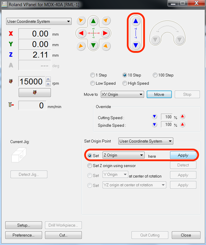
We need to set the z axis manually, otherwise the tool might break. As the cut is going to be deeper as before, the tool doesn't have to touch the surface precisely.
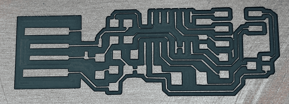
While the machine is creating the traces, make sure that the drawing of the curcuit is deep enough. Otherwise you have to stop the job and increase the depth.
As soon as the job is done, clean the surface with the vacuum cleaner to get rid of the copper and the wood dust.
Milling Problems
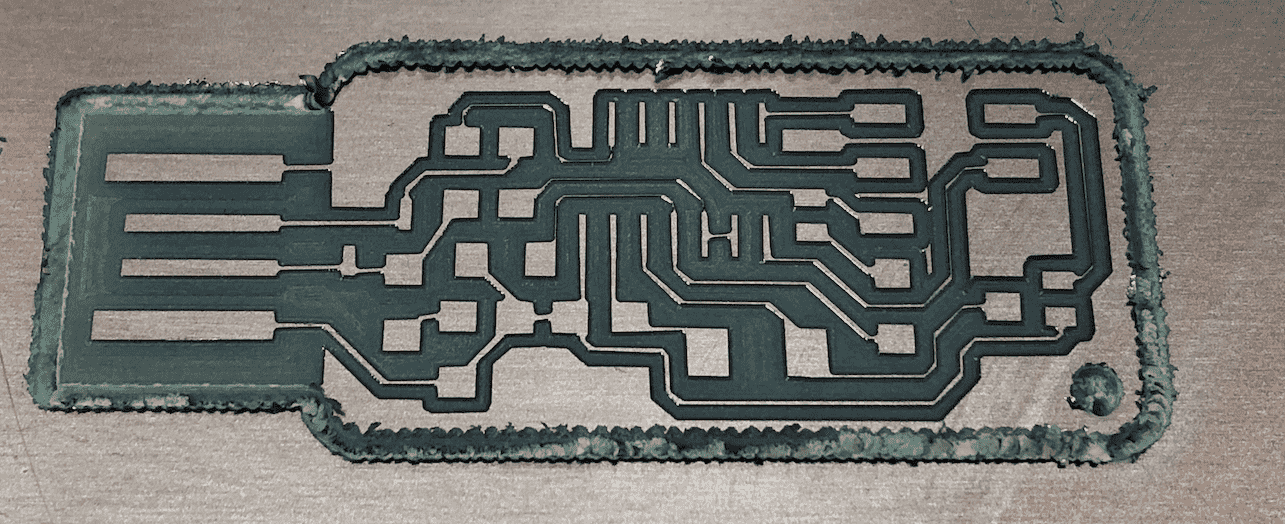
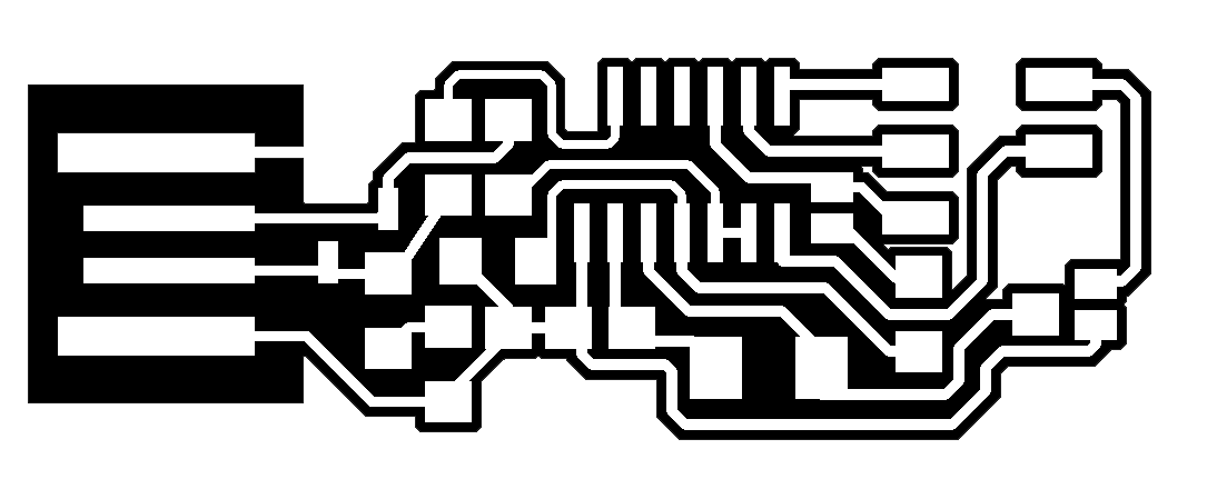
As you can see below the traces of the board are very thin. This means that they are very fragile. The traces could break easily, while soldering the electronic components on the board. So I decided to redo the board. I could mill it agian with a higher z axis, but the traces on the image already seemed to be very thin. That's why I decided to make the job easier by increasing the thickness of the traces using Gimp .
To increase the thickness of the traces, we first have to select all the traces. Through that we have a board with a ground layer, we will have to seperate the ground trace from the ground layer by creating a black rectangle. Otherwise we would increase also the outside of the board.

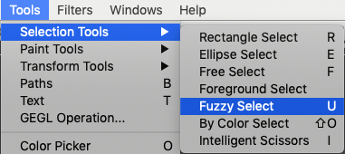
Afterwards go to tools --> selection tools --> fuzzy select and use shift to select all the traces.
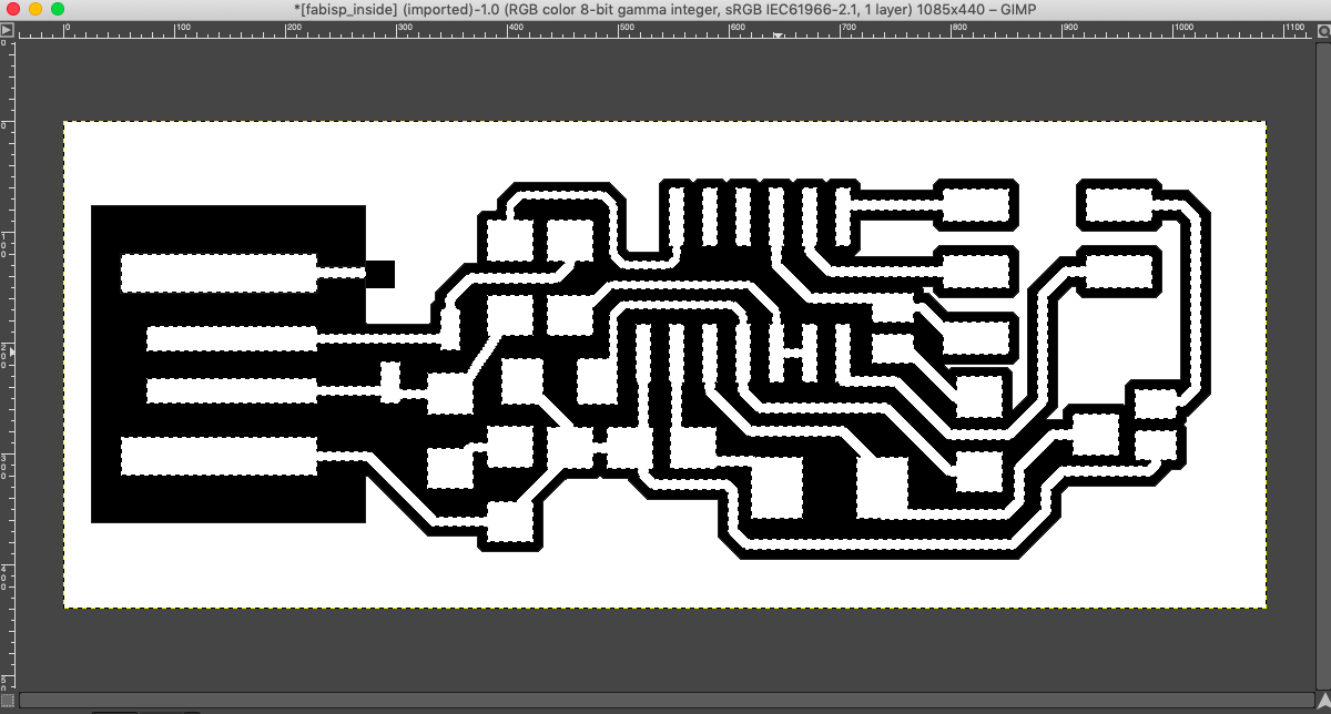
Then go to select --> grow. With this tool we can increase the thickness of the traces.
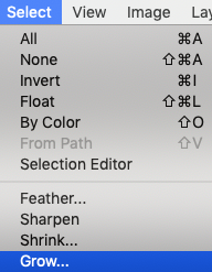
A new window will appear, where you can type in the thickness of the traces. I choose to add 2 pixel.
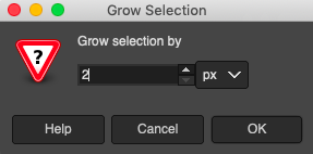
Next you have to refill them with white color usig the bucket.

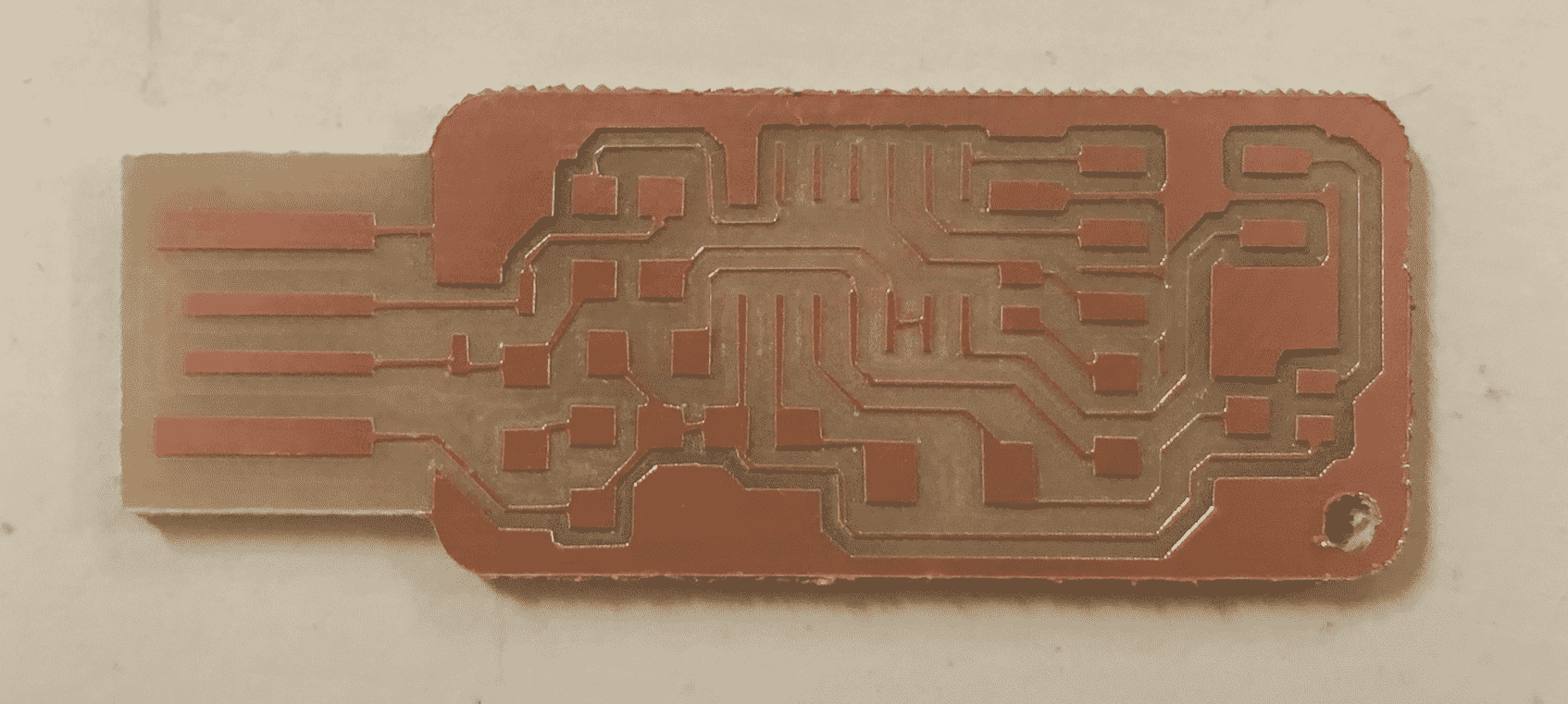
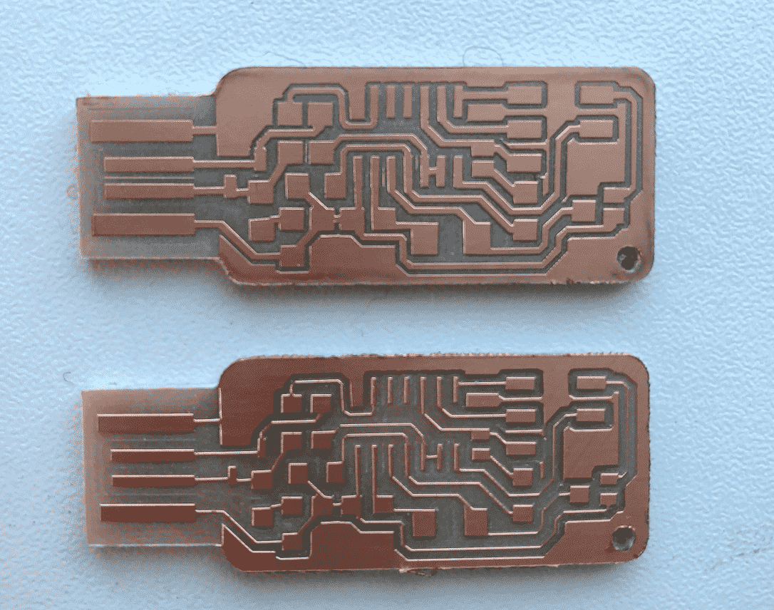
Below you can see the differences between both boards.

The picture underneath shows the result of both boards using the same configurations for the milling process on Fab Modules. I think it was very usefull to increase the thickness of the traces, because now they can be exposed to more heat without getting damaged or losing a connection between traces.
Soldering and Desoldering
In order to understand which components are necessary for the soldering, you have to download the schematic. Below you can see the schematic of the board.
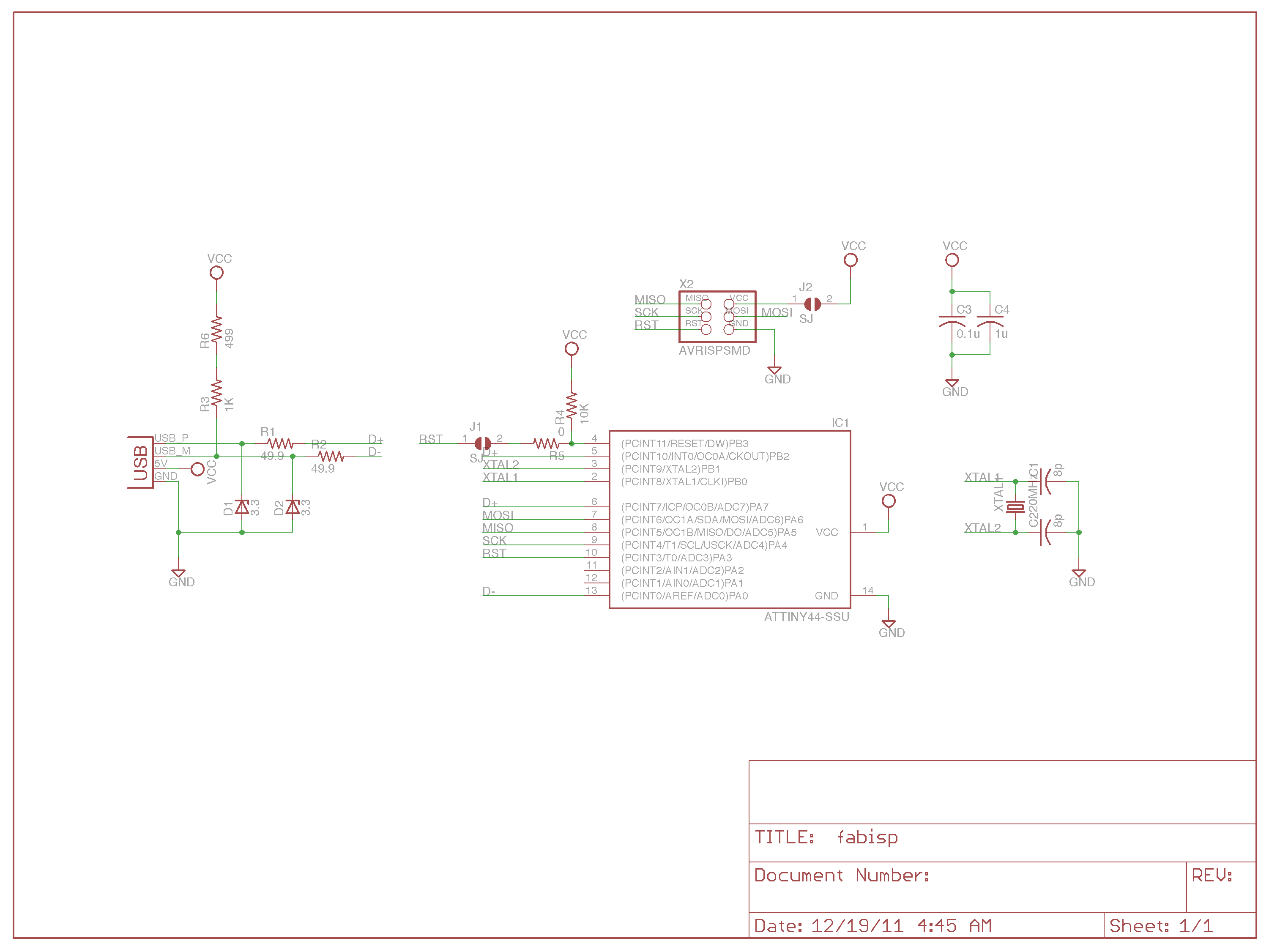
Necessary components are:
Before you start with the soldering, you need to set up the soldering iron to the necessary temperature, usually above 300 degrees. First of all we have to solder the microcontroller, as it's the most important component of the board and the most difficult one to solder. Moreover be carefull with the microcontroller, because if it's exposed to too much heat it could get destroyed and then you have to start over. Insure yourself that all the pins of the microcontroller are soldered correctly and use the multimeter consistently to check the connections. It's also difficult to attach the component to the spot you desire, ones it's attached the soldering is easier. Don't be afraid to use to much soldering material, as you can always remove it with a copper wire. To make it easier we put some soldering material on one pad, usaually one that's in the corner.
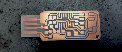
Then we place the microcontroller in the desired position. Also be aware that the microcontroller has a circile on top which indicates, in which direction you have to solder it. Just take a look in the schematic. Next you have to heat up the soldered pad, so that the soldering material can flow directly on the pin. Now the microcontroller is fixed and you can easily continue soldering the remaining pins.
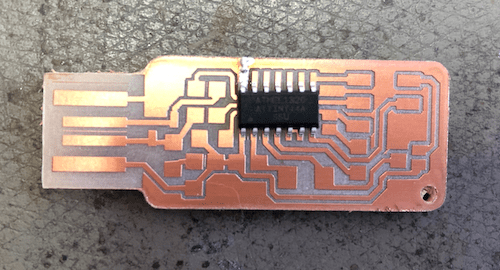
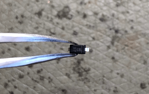
Then we are going to solder all the little components beginning from the middle of the board. At the end we solder the pin headers, as they are the biggest components. The diode has a polarity. This means that you have to pay attention, in which way you solder it. The picture underneath shows the diode. On top of the diode you can see a line. When you solder the component the line has to be on the side of the VCC.
As you can see underneath I have a cold soldered joint. Cold solder joints are unreliable. The joint will be weak and they often develop cracks over time. You can repair it by reheating it with your soldering iron until the soldering begins to flow. Or you can just remove the soldering with the copper wire and resolder the component.
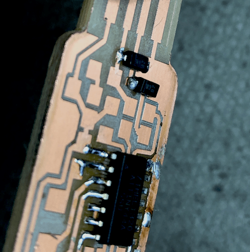
Here is the difference between a shiny soldered joint and a cold soldered joint.
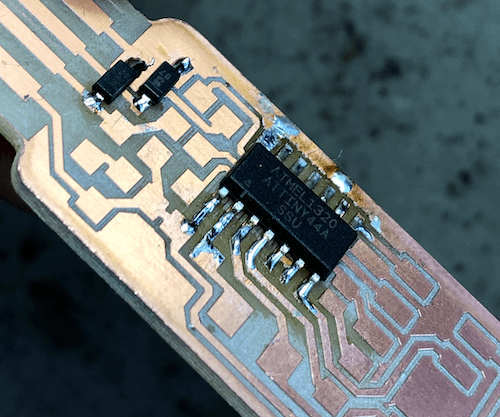
If you used to much soldering material, you can easily remove it with a copper wire. Just squeeze the copper wire on top of the soldering material and wait for it to heat up. As soon as you see, that the soldering material becomes fluid remove the wire. Below you can see a small video of the process.
Underneath I soldered everything except of the pin headers.
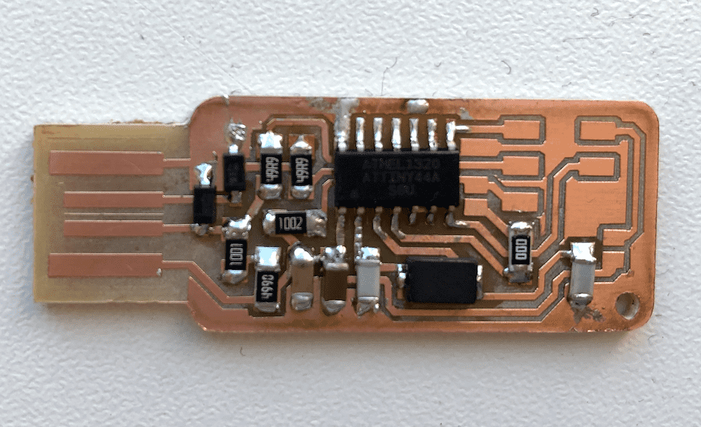
After soldering the pin headers you have to bridge the connection of the Reset pin. A brief reminder if you do not brindge the connection to the VCC pin, be aware that you will have to use a usb hub to provide the microcontroller with 5 volt. Otherwise you will get an error while programming the board.
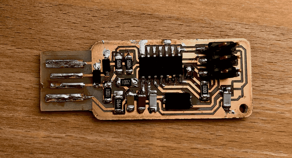
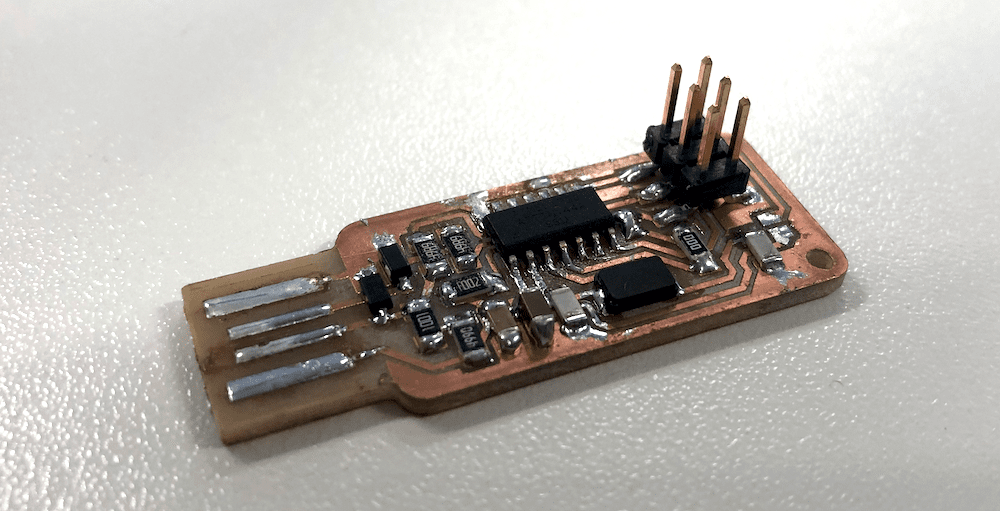
Finally check all the connections again to be sure that every pin of the microcontroller is well-connected. Moreover always be sure that you do not have a connection between VCC and GND.
Programming
To enable the FabISP as a programmer I am using a Arduino Uno board, but you could also use something else then a Arduino Uno. In order to give the microcontroller functionality, the Arduino Uno needs to act as a programming board. For a start you need to connect the Arduino Uno with the PC and open the Arduino Software. Identify the board as Arduino Uno by going to tools and select the proper port.
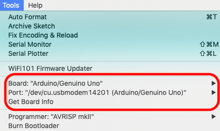
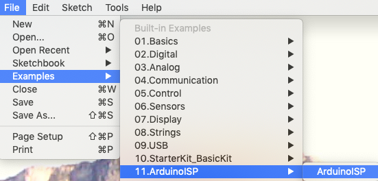
Thereafter you need to open the file that makes the Arduino board act as a programming board. Go to File --> Examples and open the ArduinoISP program.
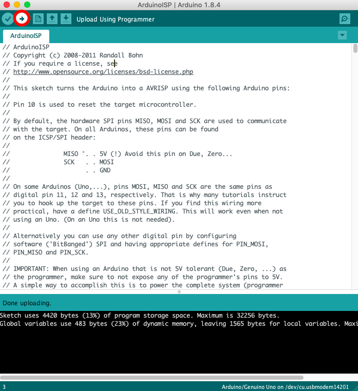
Then verify and upload the code to the Arduino.
Before connecting the PCB to the Arduino Uno, check all the connections with the multimeter, to be sure that you have a closed circuit and that you do not have any shorted circuit.
If everything is well-connected, you can go ahead and connect the PCB with the Arduino.
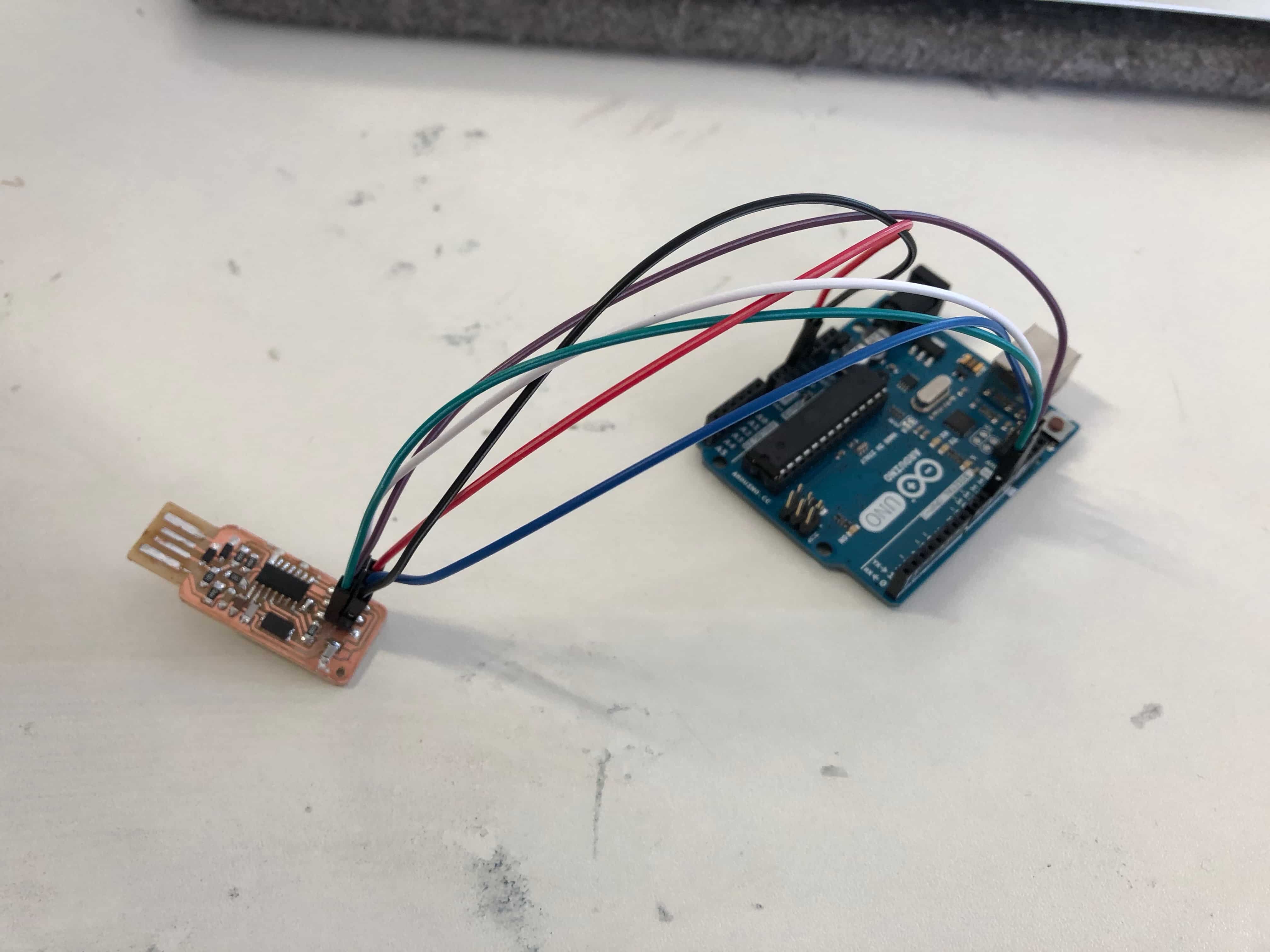
If you didn't bridge the VCC connection you need additionally to connect the PCB to a usb hub to provide the microcontroller with 5 volt.
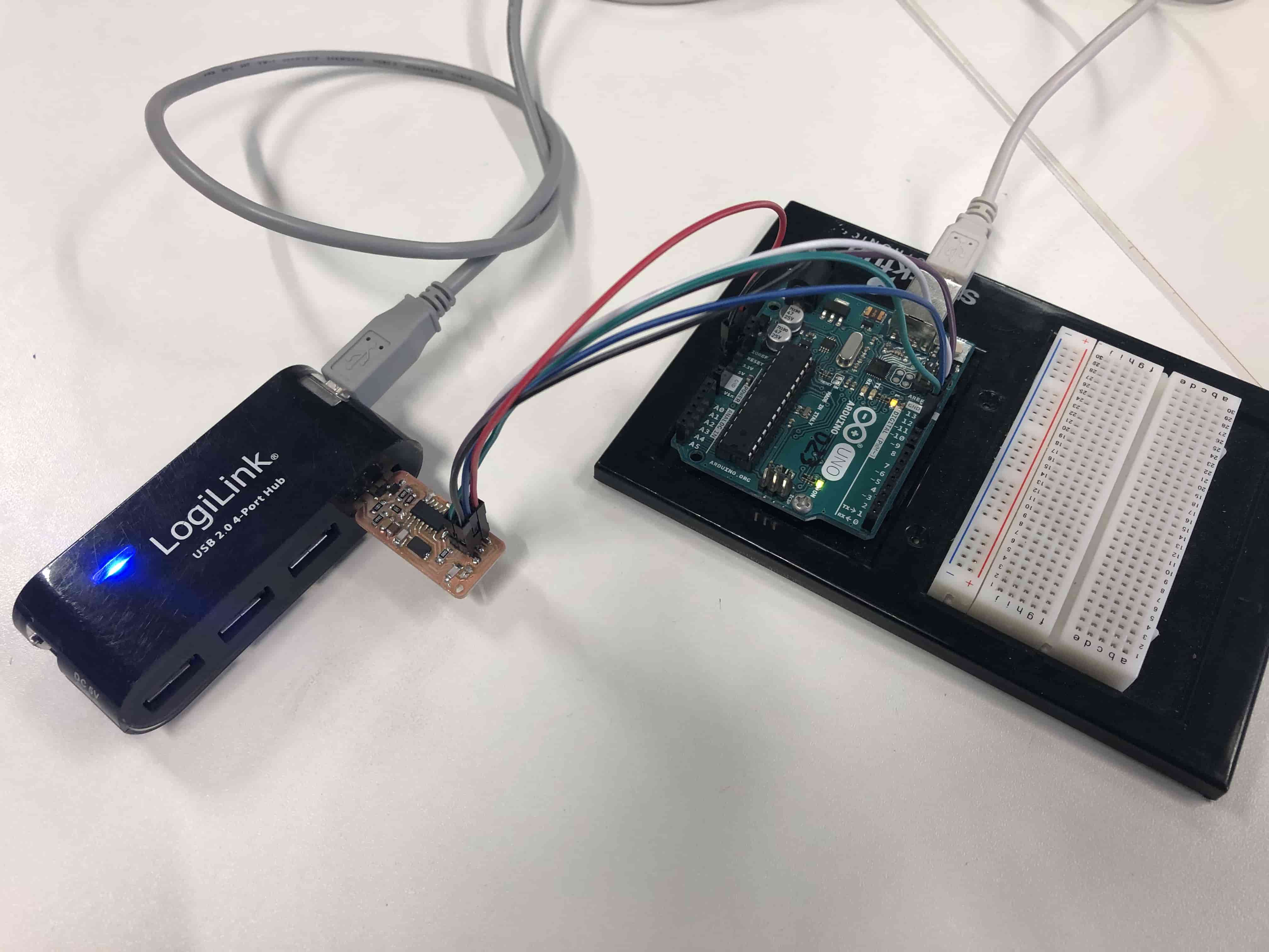
To program the FabISP, you first need to install the necessary software for your operating system and download the firmware. Since I am using a Mac, I will need to install the following software:
Here you can find the FabISP Firmware for MacOS
After downloading and installing everything, open the terminal. Next we have to edit the Makefile. Therefore we have to change the directories to open the Makefile in the terminal. To move around the file system you use cd.
cd Desktop/firmware/
Now we have to modify the Makefile. The Makefile is set up to work with the AVRISP2 by default. To open it use the next command:
nano Makefile
Now go to the line that says:
#AVRDUDE = avrdude -c usbtiny -p $(DEVICE) # edit this line for your programmer
AVRDUDE = avrdude -c avrisp2 -P usb -p $(DEVICE) # edit this line for your programmer
Here you will have to add a "#" before both lines, so that they will be excluded.
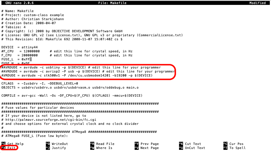
Furthermore you have to add the following line: AVRDUDE = avrdude -c stk500v1 -P /dev/ttyACM0 -b19200 -p $(DEVICE) and change the port to the actual port, to which your Arduino is connected to. To find out which port it is, look under tools in the Arduino Software. Finally save the file.

Next you need to compile the firmware.
make clean
If you are successful, you will see this response from the system:

make hex
If you are successful, you will see this response from the system:
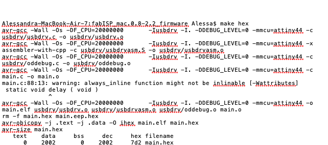
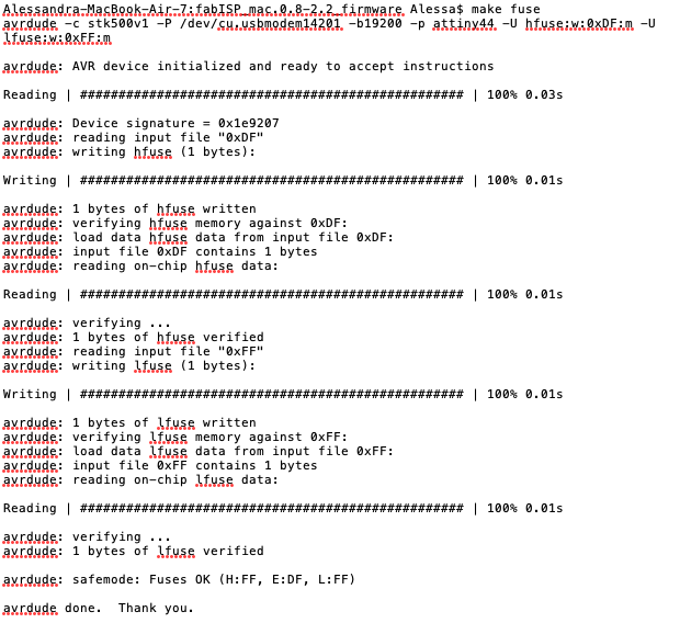
Next, you need to set the fuses so your board will use the external clock (crystal).
make fuse
If you are successful, you will see this response from the system:
make program
If you are successful, you will see this response from the system:
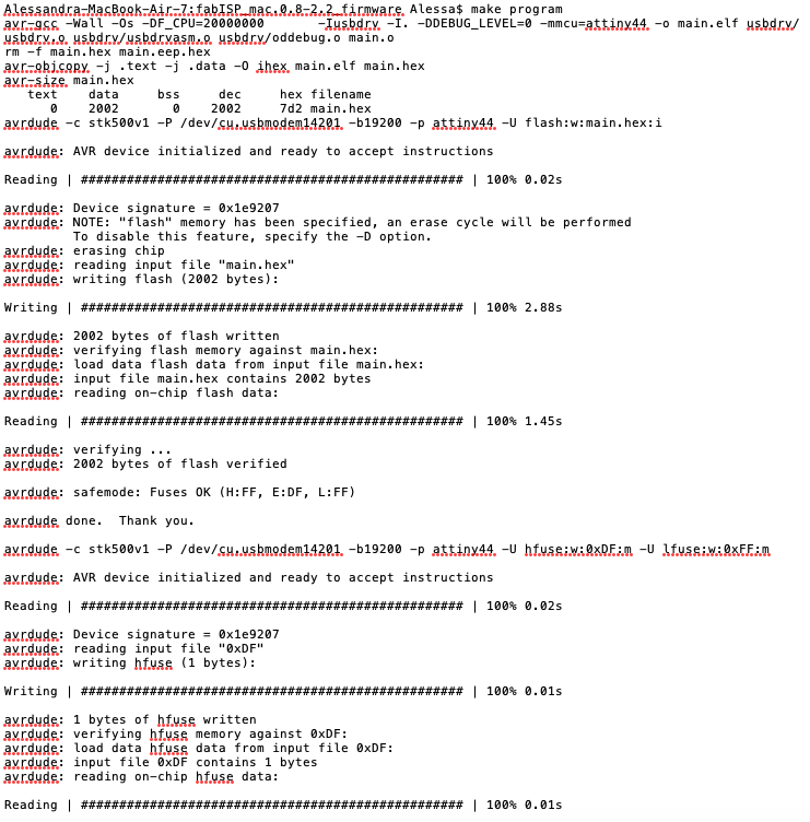
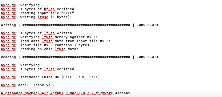
To check if everything worked, you have to plugin the PCB into you usb port without an Arduino. Don't plug it in without using a hub, if you think the PCB might have a short circuit. Because then you might burn your computer.
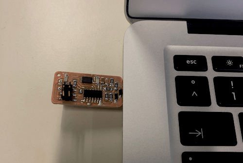
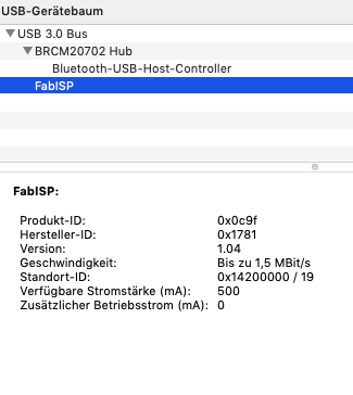
Check the usb port of your operating system. If you see the FabISP, then the programming was successful.
Finally you have to unsolder the Jumper, which we needed to programm the board.
Download Files
PNG-Files
FabISP insideFabISP inside improved version
FabISP outside
RML-Files
FabISP insideFabISP inside improved version
FabISP outside