
This work is licensed under a Creative Commons Attribution-NonCommercial-ShareAlike 4.0 International License
Week 14: Networking and Communications
May 2, 2021Summary
This week's assignments
- Group assignment:
- Send a message between two projects and document your work
- Individual assignment:
- Design, build, and connect wired or wireless node(s) with network or bus addresses:
- Document your project ✔
- Document what you have learned from implementing networking and/or communication protocols ✔
- Explain the programming process/es you used ✔
- Outline problems and how you fixed them ✔
- Include design files (or linked to where they are located if you are using a board you have designed and fabricated earlier) and original code ✔
Resources Used
- Software: KiCad, Arduino IDE
- Hardware: Roland SRM-20
Skills Gained
- I2C Communication
My Weekly Schedule
Experimenting with the I2C Network
Part 1: Testing the I/O devices on Arduino
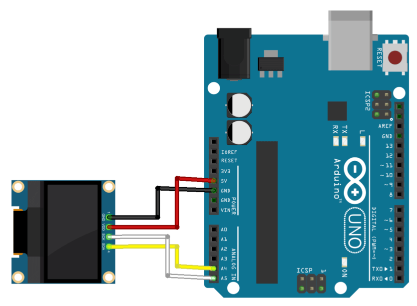
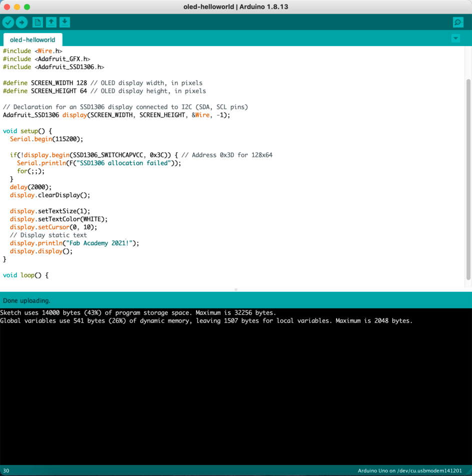
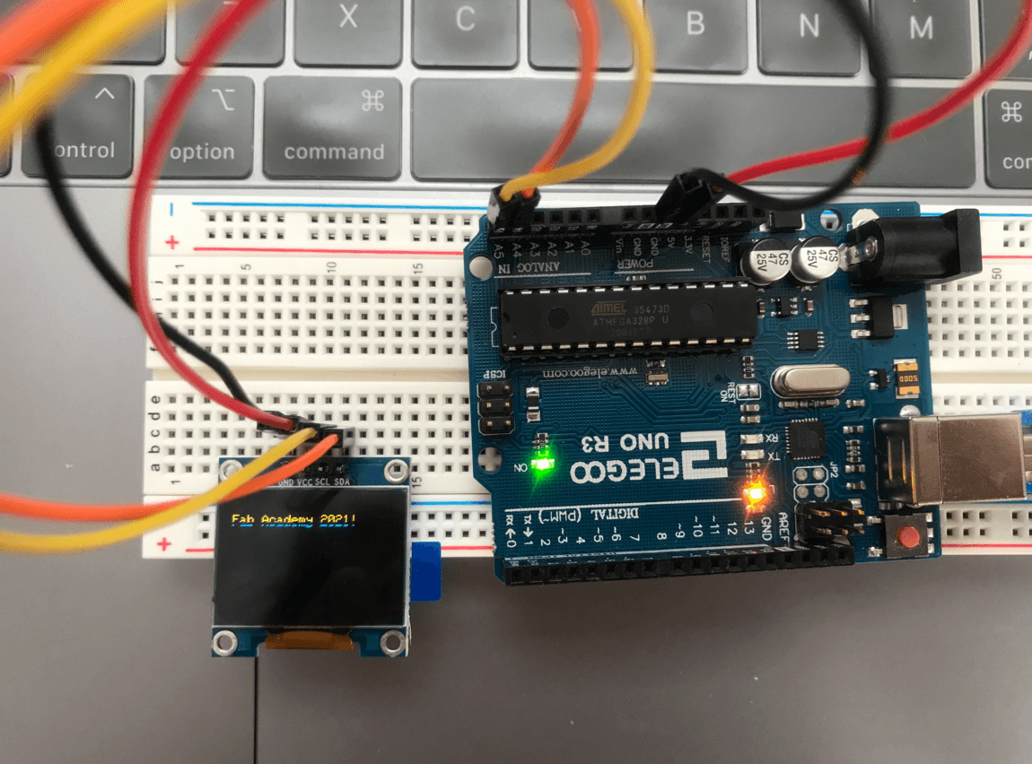
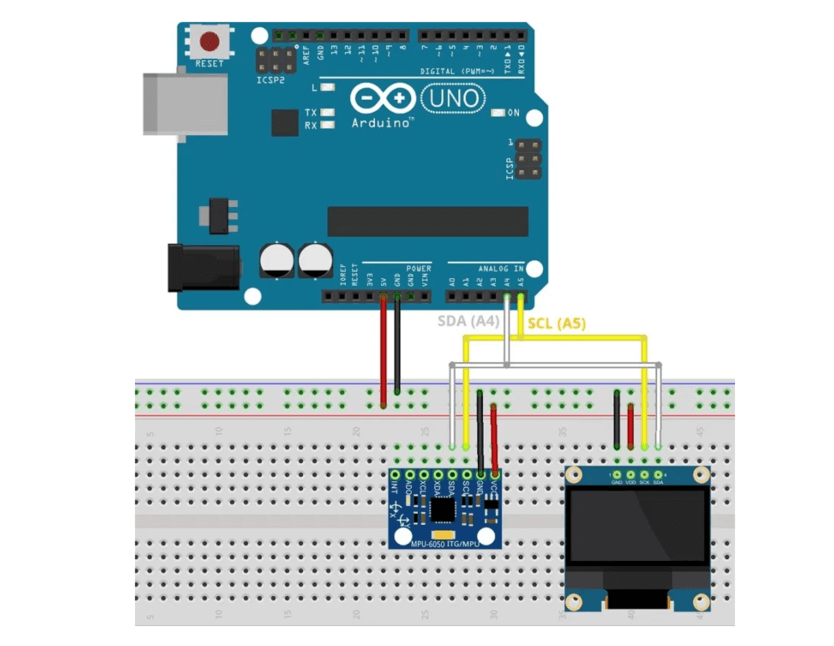
May 1, 2021OLED Display + Arduino
setup
sketch
result
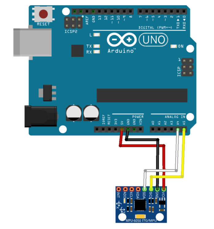
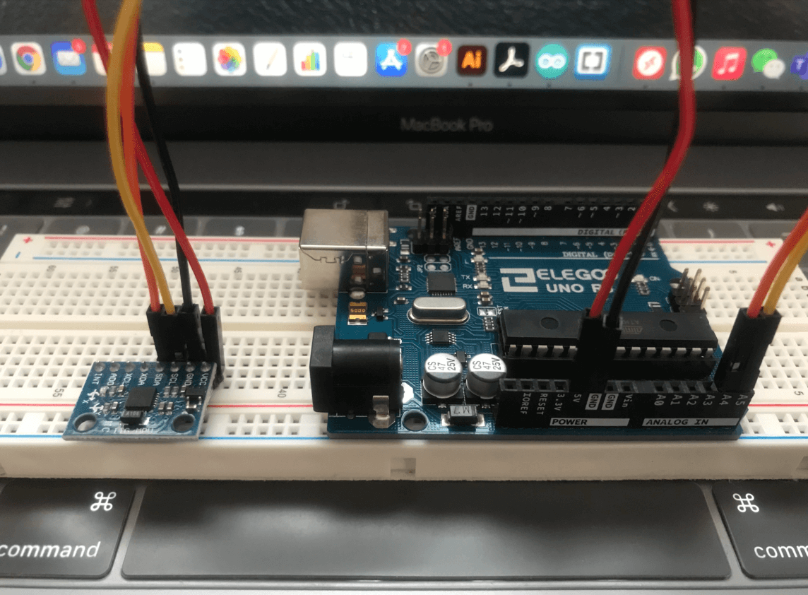
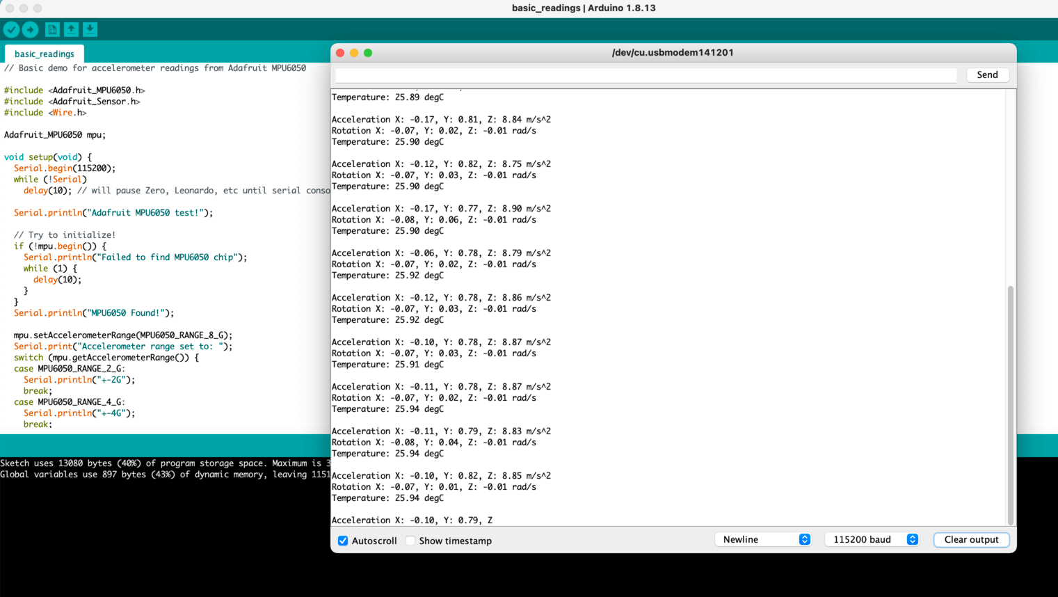
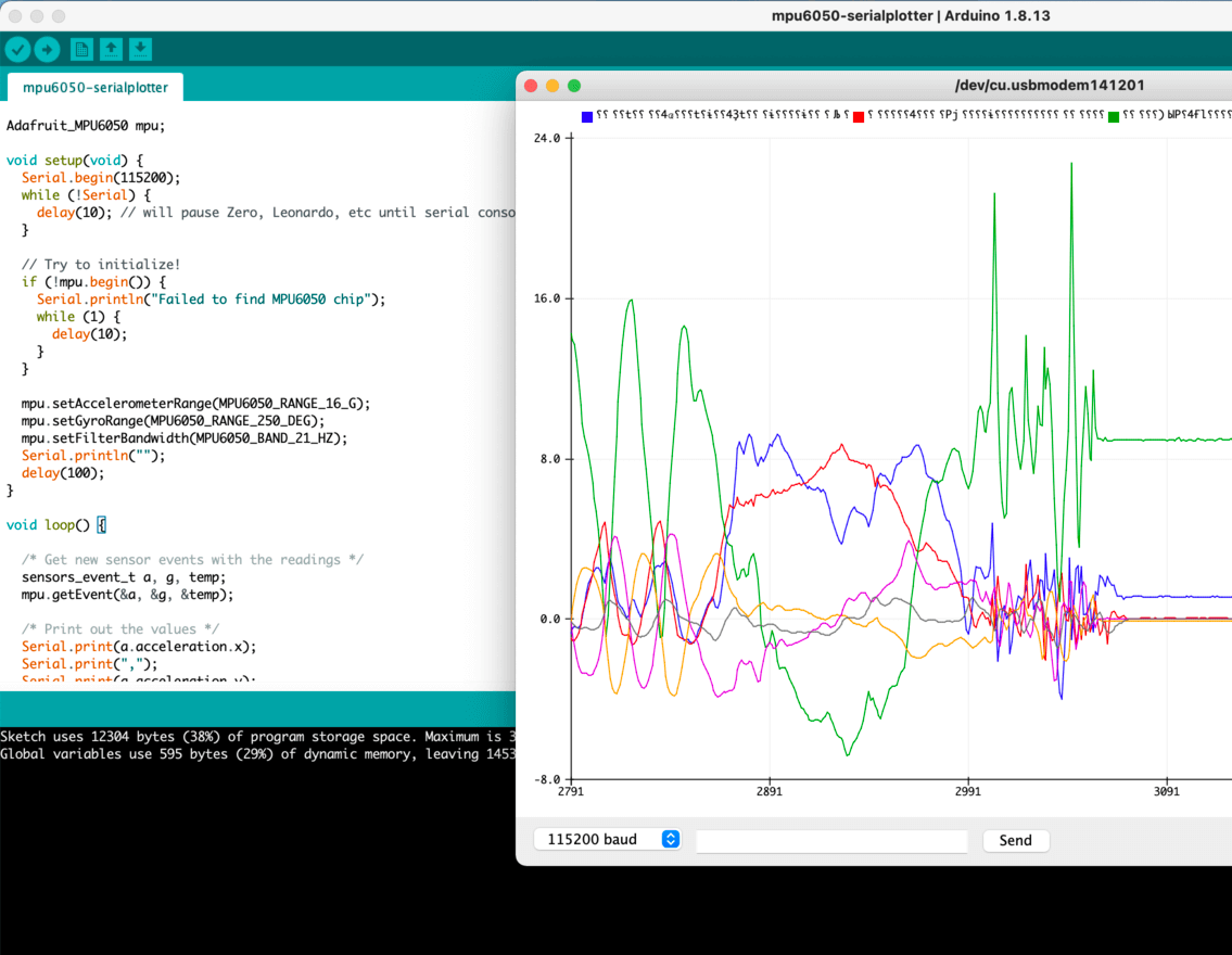
MPU-6050 Accelerometer and Gyroscope Sensor + Arduino
setup
serial monitor
serial plotter
MPU-6050 Readings on OLED Display
setup
sketch
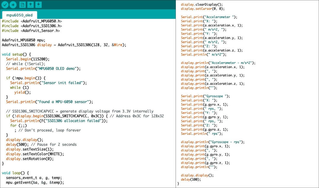
result
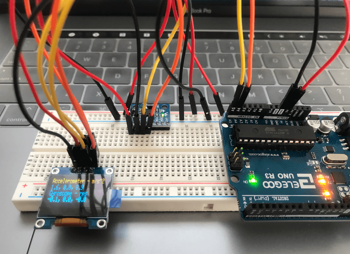
Here is a short video showing the MPU-6050 reading on the OLED display:
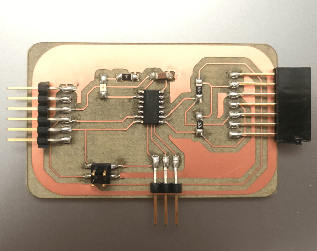
Part 2: PCB Design and Production
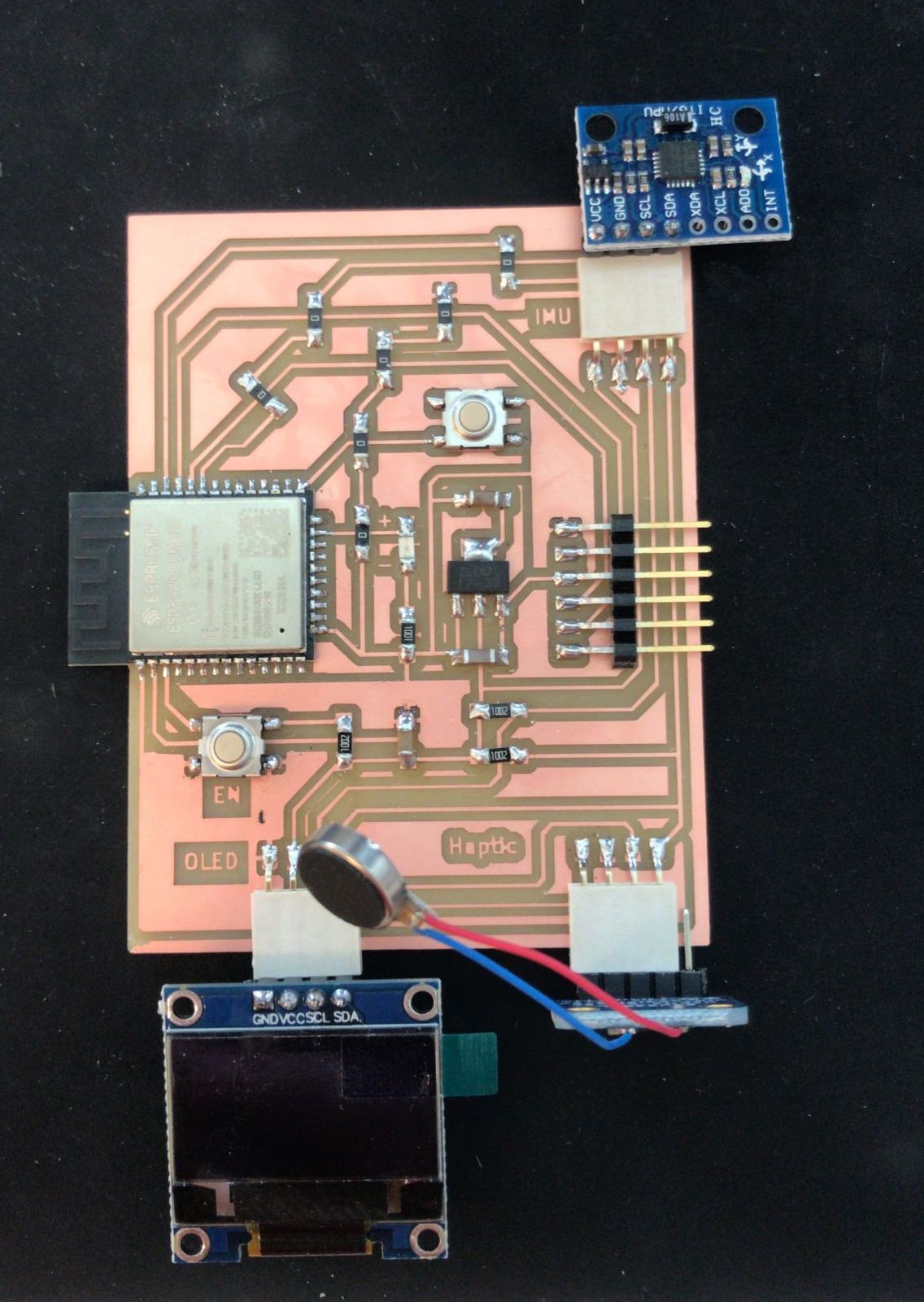
input device board (master board)
April, 30 2021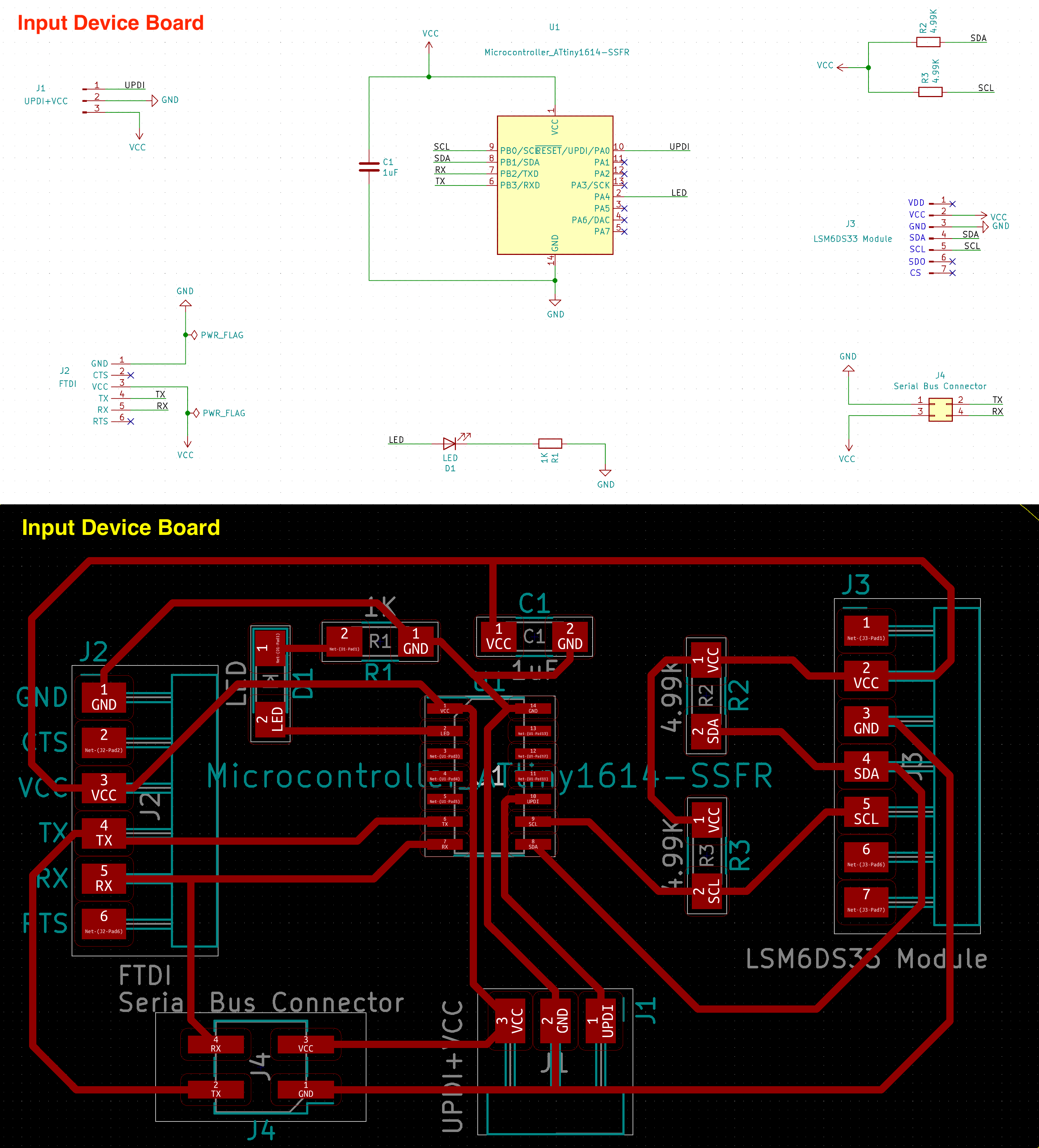
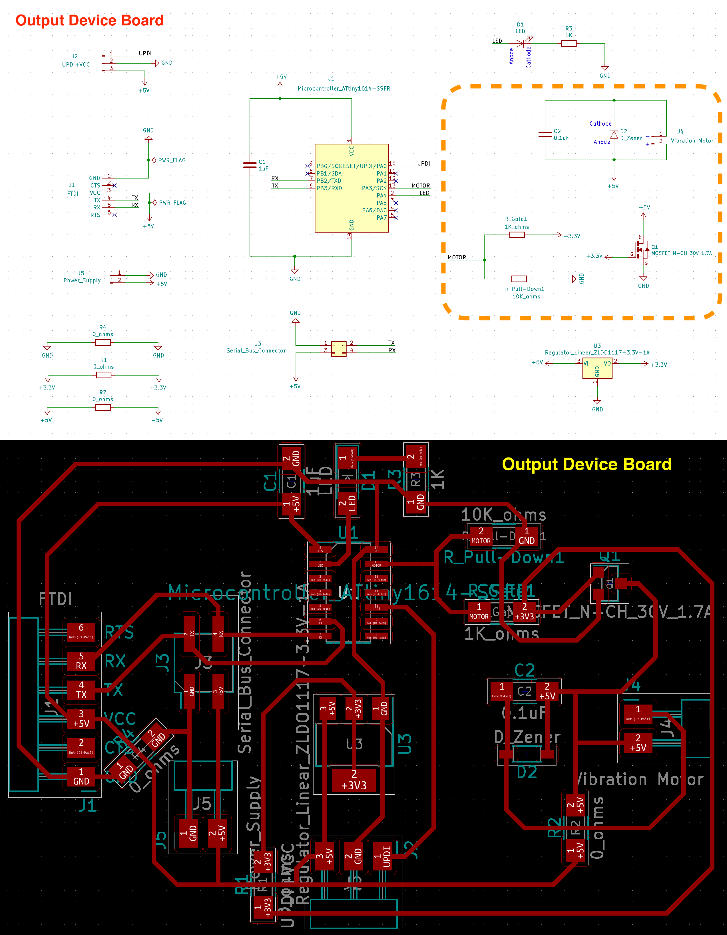
output device board (secondary board)
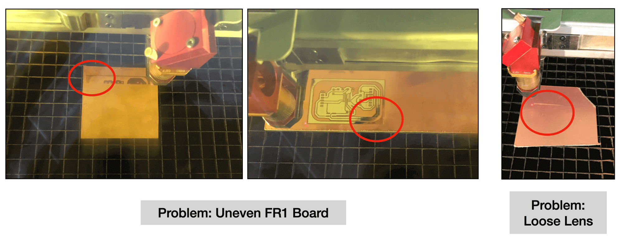
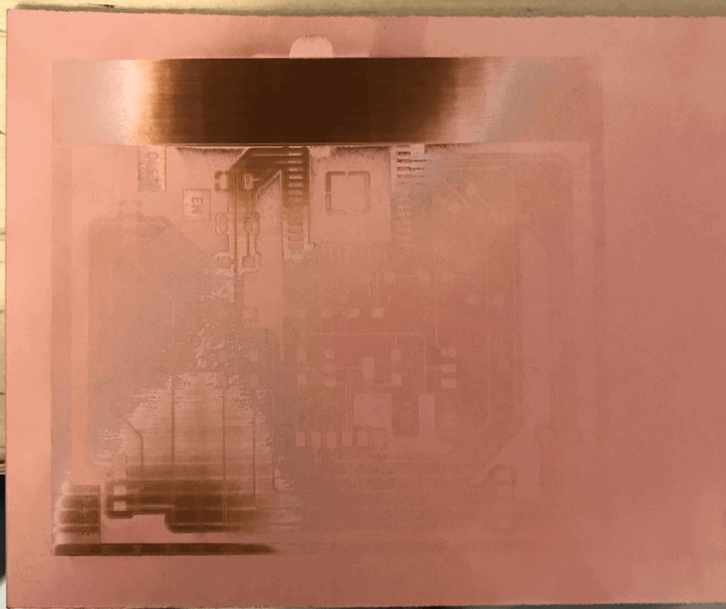
laser cutting attempts
May 3, 2021
On Monday, Spencer taught me how to troubleshoot the focusing issue on the FR1 boards. He designed a small engraving file and tested it on the two far corners indicating the size of a PCB file that I usaully have. Here is a short video of the testing. We found that even though the boards were flat, the focus was not even on four corners.
Spencer told me that it could be a problem with the apenture. In order to rectify this issue, he set up two sets of parameters (one for FR1 no cut, and the other for FR1 cut only) on JobControl, and also increased the engraving pass from 6 to 8. This method also helped remove the "copper hair" that Neil talked about during last week's lecture.
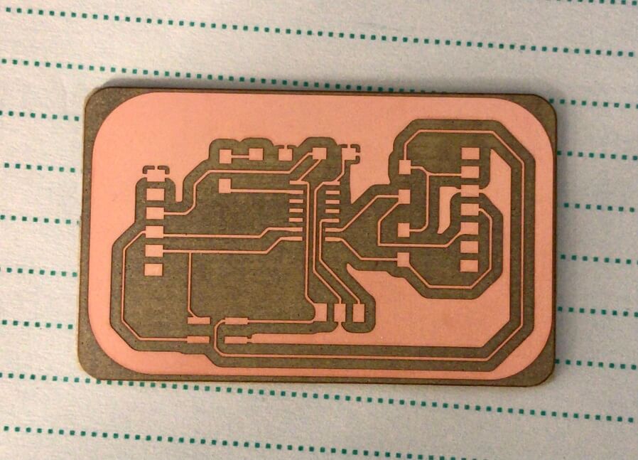
As the number of passes increased, the machining time also increased. For the input device board, the estimated engraving time was 53 minutes, and the cut time for the outline was 9 seconds. Despite taking a longer time to machine, the end result was beautiful. Here is how the milled board look:
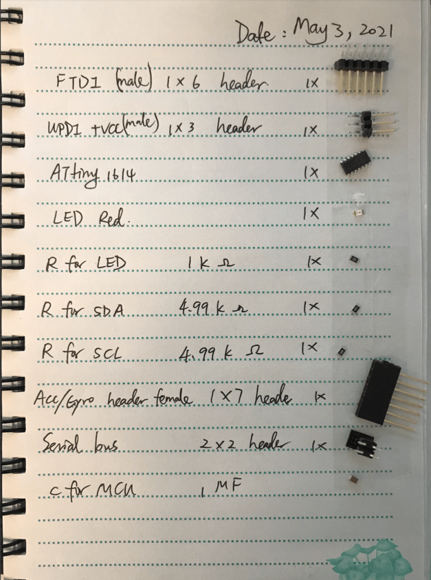
Here is the list of components needed for the board:
Here is how the soldered board look:
After finished cutting the input board, I was ready to cut the output board, however the estimated engraving time was 71 minutes! As it was almost 5pm, I decided to fabricate my output board sometime later this week instead, and used the board that I got for the moment.
During the office hour, Spencer showed me how to use the desktop power supply to check which voltage level worked better on the vibration motor, specifically we compared the performance of the motor using the 3.3V and the 5V. I liked the performance by the 3.3V better (which was already quite vibrant to me), in addition, I was already looking to build a board using the ESP32, which is operated under a 3.3V environment. Here is a short video of the vibration motor test.
May 4, 2021
Since I only had one board with me, I chose to test each of my input devices and output devices one by one as I was not able to do so successfully in the previous weeks. First, I set up the wiring like this:
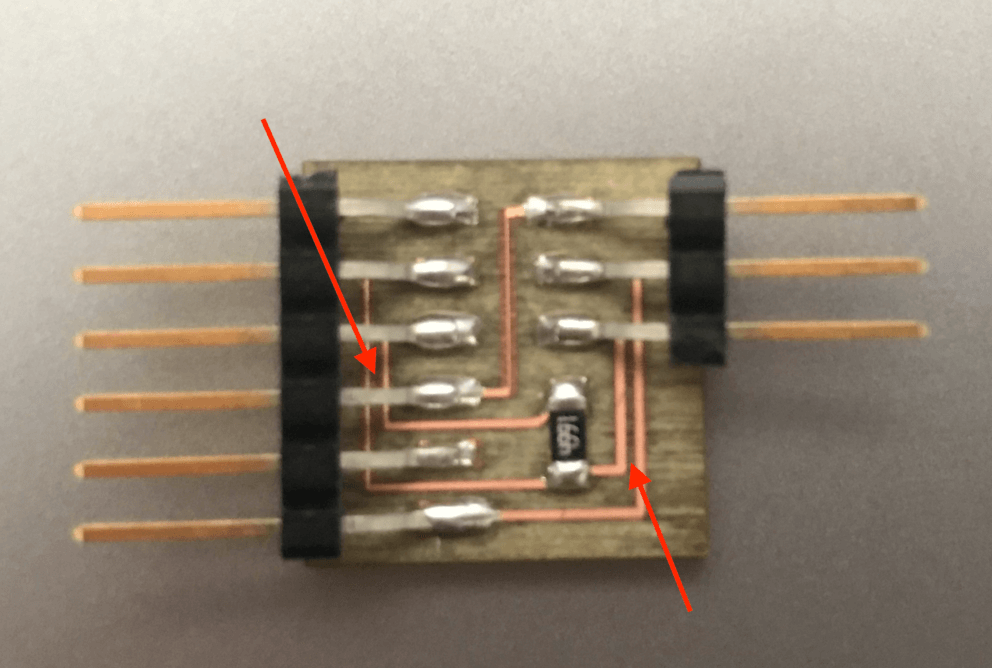
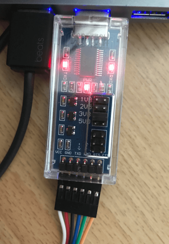
However, when I plugged the boards to the USB hub and uploaded the sketch to Arduino, I was greeted by the same error that I got in the previous week: "the board was either not connected or does not exist while the power indication LED for FTDI was also off. I didn't see any bridge on my soldering, and I knew that the connection on the board was correct, so I asked my classmate, Nick for help. He told me that the power on the FTDI adapter should be on as long as it was plugged int othe USB port, regardless of what it was plugged into. Unless there was something on my board causing a short circuit that was shutting down my USB port. He suggested me to check with a multimeter on every board to make sure there was no connectivity between VCC and GND. And he was right, the my UPDI+VCC adapter had connectivity between the VCC and GND, I fabricated this board last week. There was some copper hair left in between TX and RX traces on the FTDI (left side of the pins), and UPDI and GND (right side of the pins).
I used a tweezer to remove the excess hair and tried again, this time the power indication LED on the FTDI was back on! After solving the issue, I was ready to test the boards on my devices. First, I tested the LSM6DS33 3D Accelerometer and Gyro module:
But as soon as I plugged the module into the board, it became very hot, so I unplugged everything and lowered the FTDI voltage from 5V to 3.3V. I decided to perform the tests only on 3.3V.
May 10, 2021
I revisited the LSM6DS33 Accelerometer/Gyro module using this board, and was able to get it worked for the 3.3V FTDI supply voltage. When I created the PCB design for this board, I intentionally flipped the FTDI so the GND pin was the last pin instead of the first pin. Since the Accelerometer/Gyro module required the Serial in Arduino, I would need to remove the UPDI adapter after verifying succesful upload to Arduino. However, I realized that, I had to connect the TX node of the FTDI to TX node of my board, and RX node of the FTDI to RX node of my board to make it work... this was unusal because normally, at this stage, I should connect TX of FTDI to RX of my board, and vice versa.
At first, I thought that I was not supposed to flip the header, but then I realized that, during the PCB design, I have connected the TX and RX pins of ATtiny1614, to RX and TX pins of the FTDI. Now that looking back, I think this would be better especailly for the ESP32 board that I am making, because it does not require UPDI adapter so it would be better if I don't have to change wires when working with the Serial in Arduino IDE after verifying the sketch upload.
I was happy I got this board work! Here is a short video featuring the board and the module.
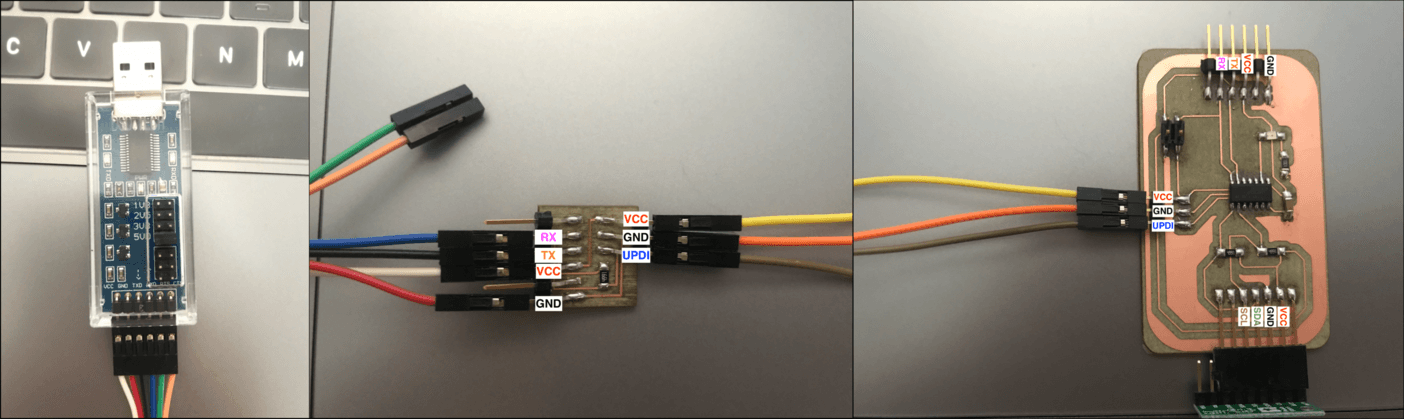
As a note to my future self, the connection for this board would be as follows:
- For uploading the sketch - Use FTDI + UPDI + this board:
- FTDI pins (1 x 6 header): Connect GND, VCC, TX, RX of FTDI to the same pins of UPDI
- UPDI + VCC pins (1 x 3 header): Connect GND, VCC, and UPDI of UPDI to the same pins of my board
- After verifying upload - Use FTDI + this board:
- Remove UPDI from FTDI
- FTDI pins (1 6 header): Connect GND, VCC, TX, RX of FTDI to the same pins of this particular board (Reason: I flipped FTDI header during the the PCB design stage)
- Open Serial monitor / serial plotter to check for results.
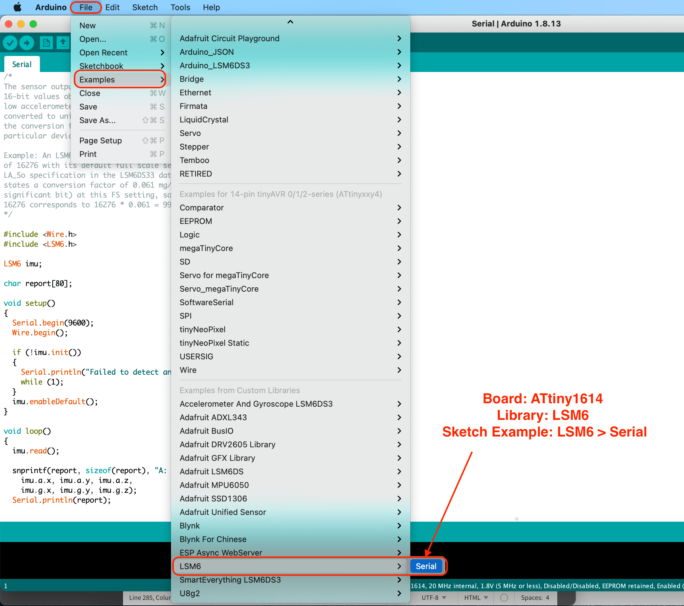
And the Arduino sketch that I used to test the board/module was the Serial example sketch by LSM6.
May 4, 2021
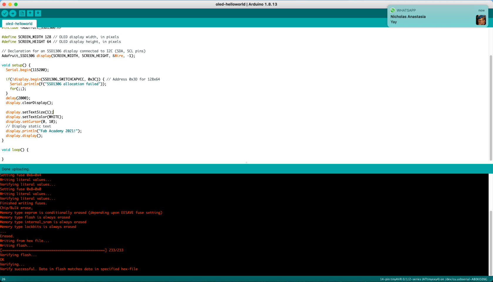
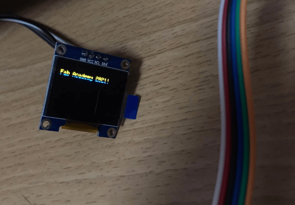
Next, I tested the OLED display. I used the same sketch previously and once it finished uploading, the "Fab Academy 2021!" text appeared on the screen. Yay it worked!
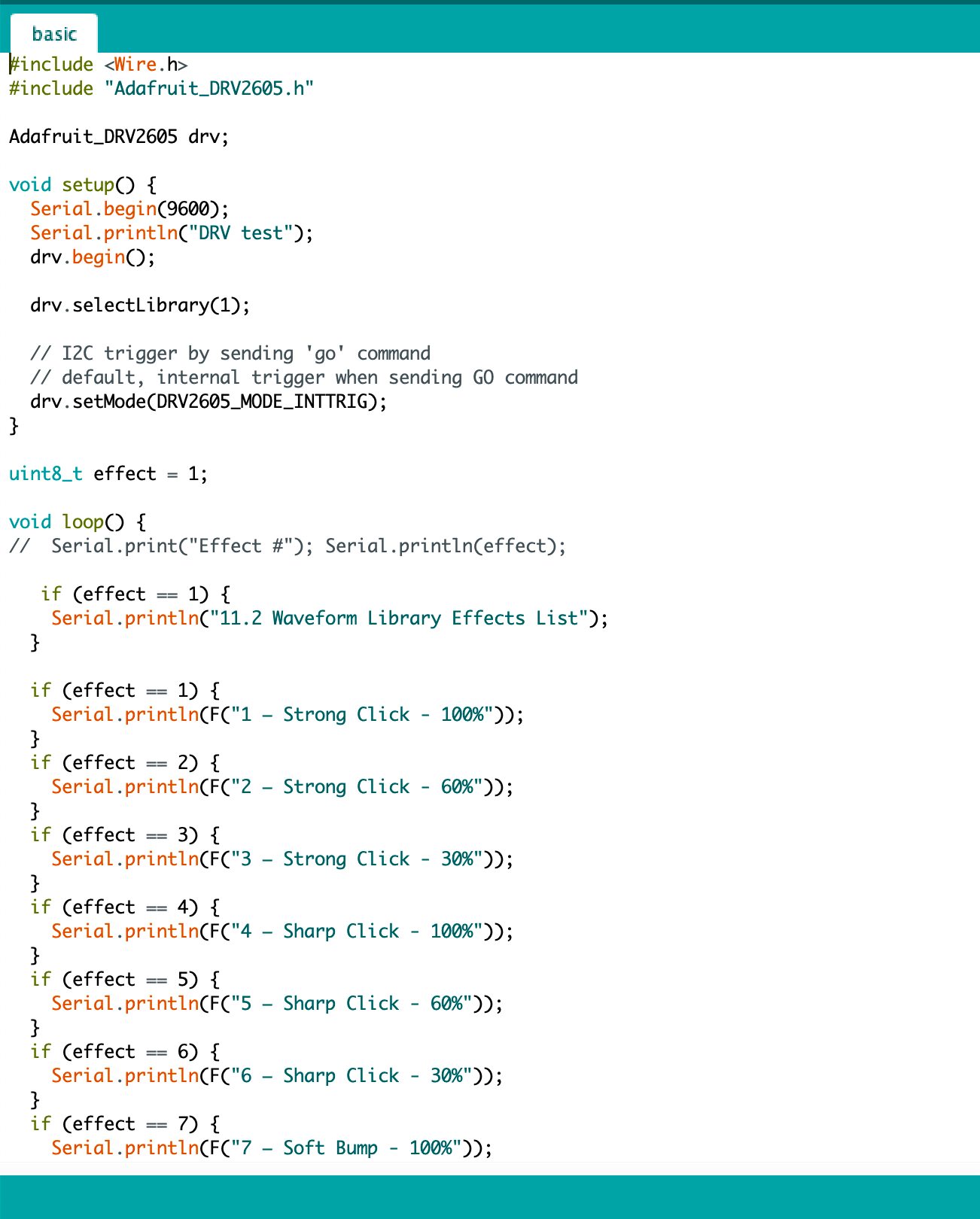
Over the weekend, I received the Adafruit Haptic Feedback board for the ERM vibration motor, as it used I2C communication, I decided to test it on my board to see if it wored, and it worked too! Here is the sketch by Adafruit and a short video featuring the vibration motor:
I noticed that it took much longer to upload the sketches to my board (almost 5 minutes) than to Arduino (10 seconds) because my board required the UPDI adapter. I saw that taking this long was not ideal for the final project, and as I had envisioned to use bluetooth, I proceeded with designing a new board with ESP32-WROOM-32D or ESP32-WROOM-32E as the processor.
Using ESP32 for Final Project
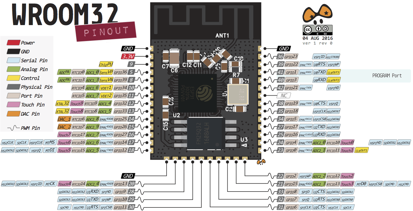
May 4, 2021Wroom32 pinout
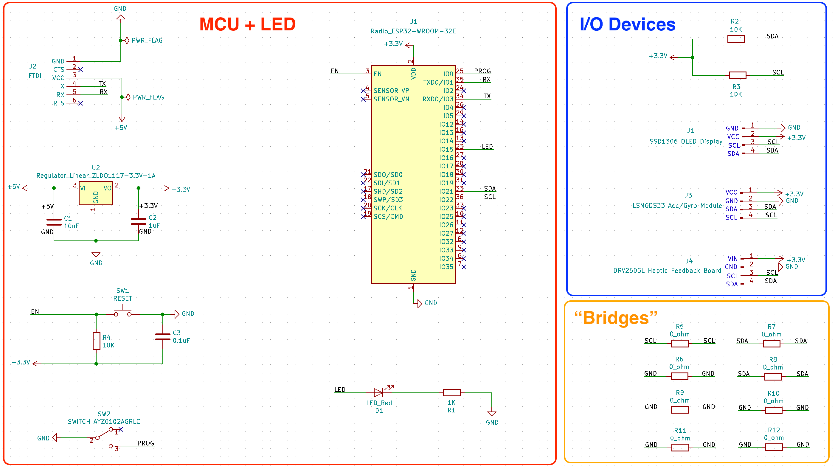
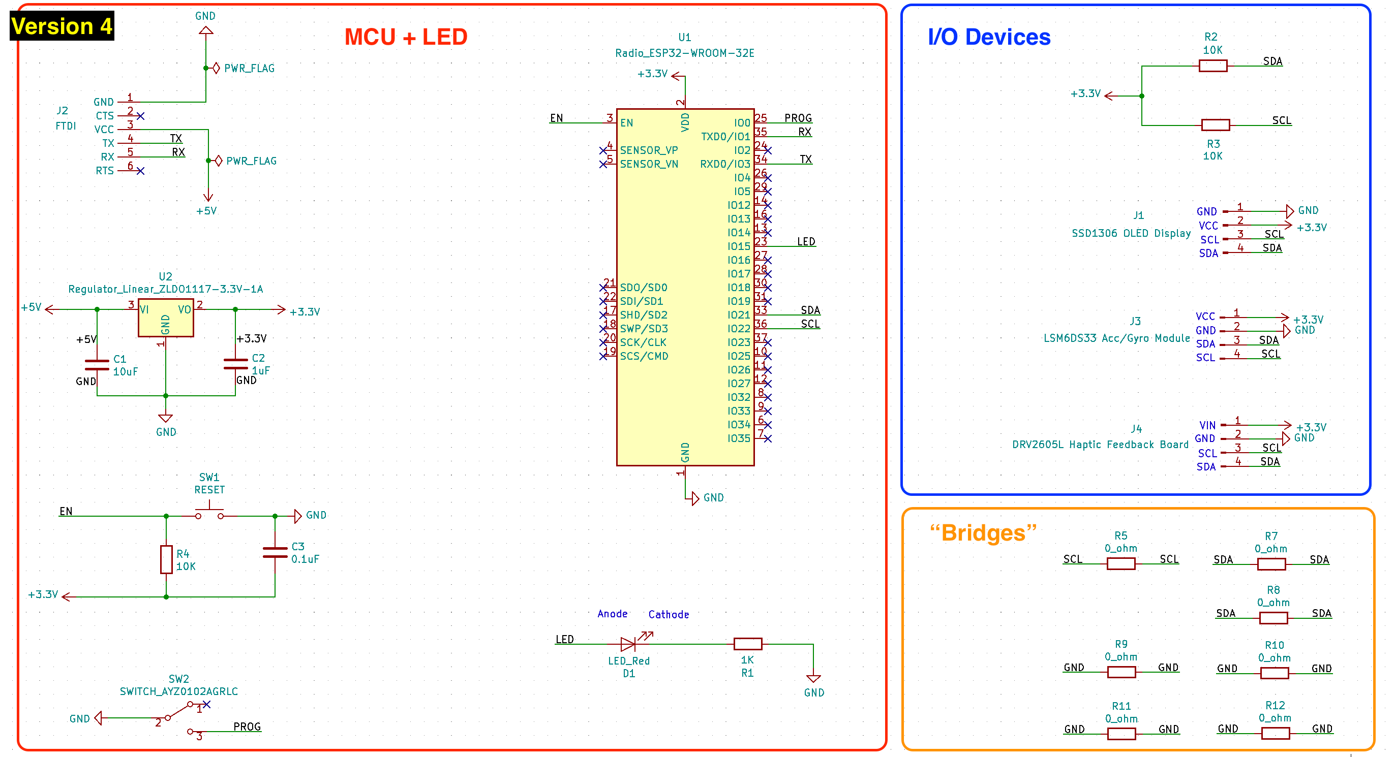
PCB design Version 1: inspired by Griffin's design, I put all my I/O devices into one board:
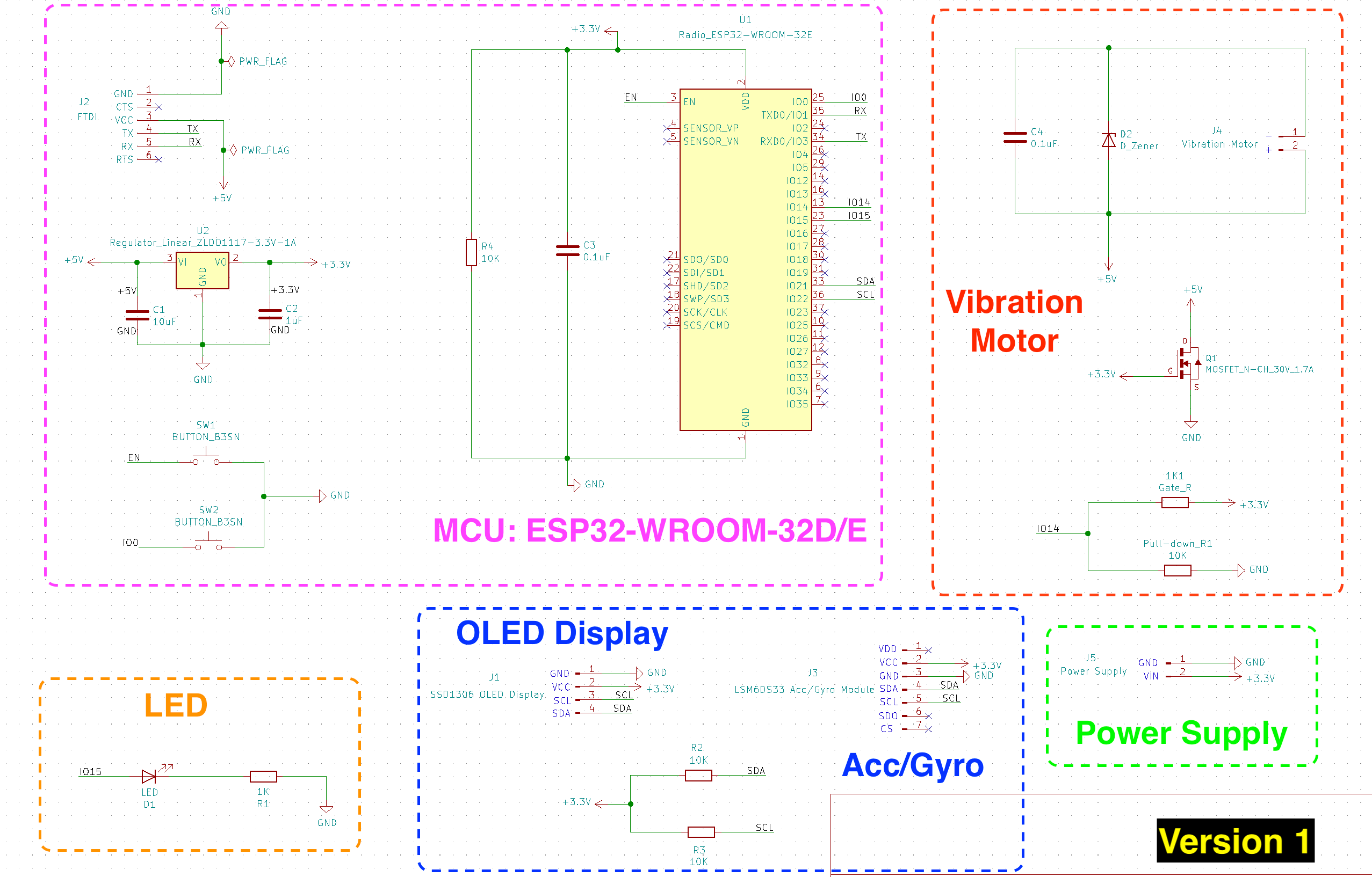
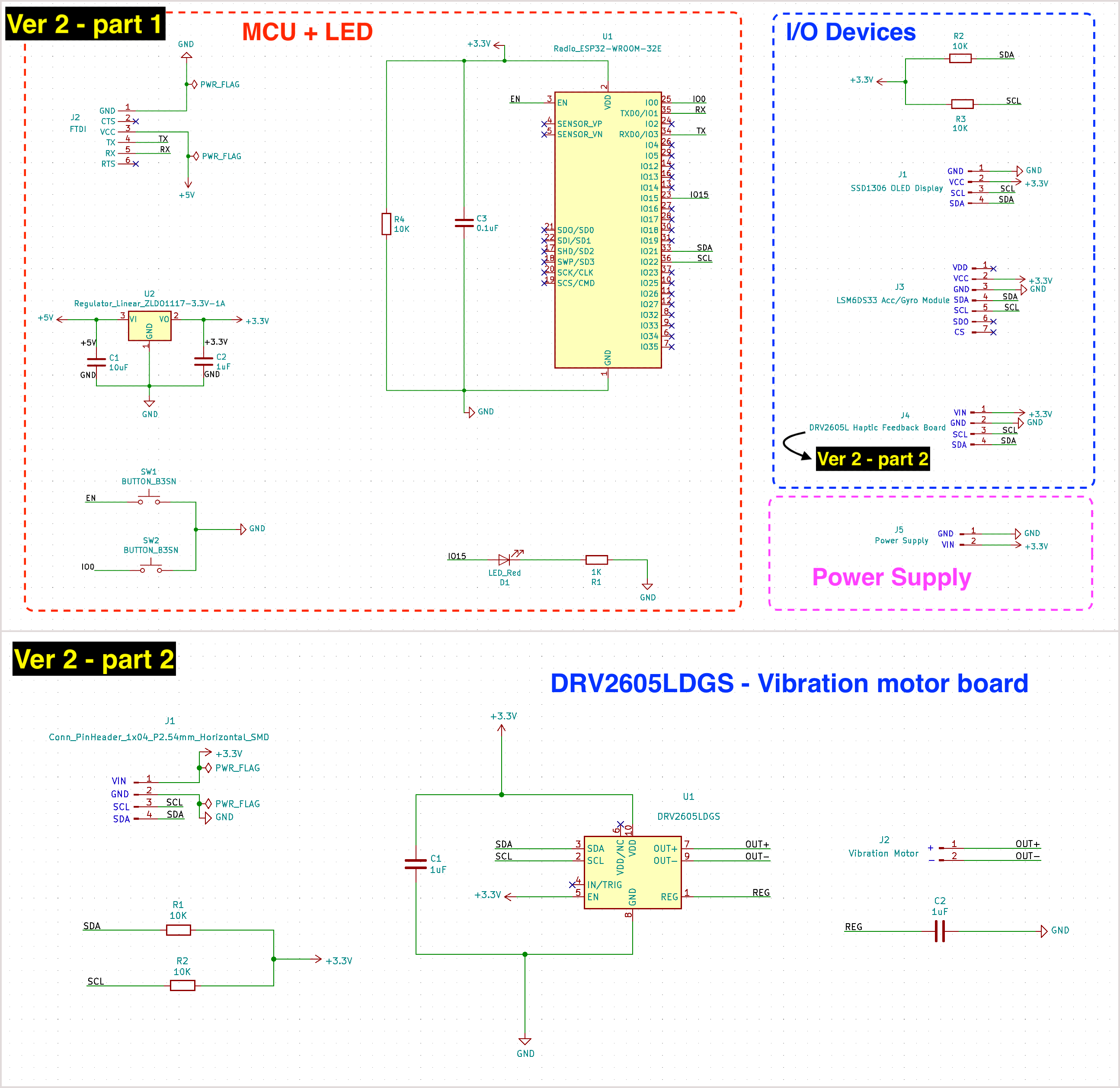
Version 2: notice that I replaced the vibration motor in version 1 with a "haptic feedback board", the one that I was planning to use was Adafruit's Haptic motor Controller as I could use the SDA and SCL pins for I2C communication. In the second image, I reproduced Adafruit's PCB design for this board using KiCad.
May 6, 2021
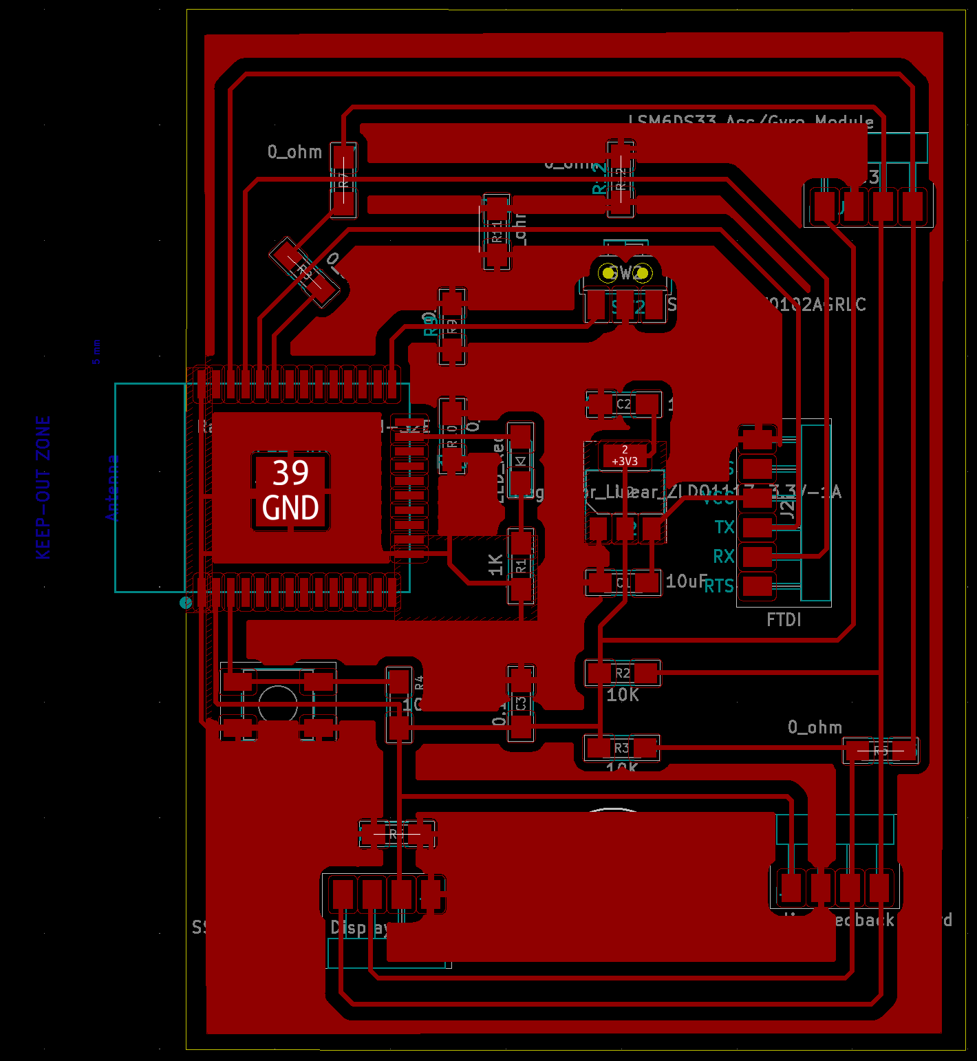
Version 3: 1) Fixed the schematic errors that I made and added eight 0 ohm resistors as the bridges; 2) removed the power supply since I was not sure if the battery alone would work for the system; 3) replaced the ESP32-WROOM footprint with the one in Barduino 2.2 in order to pass the electronics rules check.
Please note that this layout may only work for non-flex PCB production process, since the small pads may struggle staying on the sheets during the weeding process.
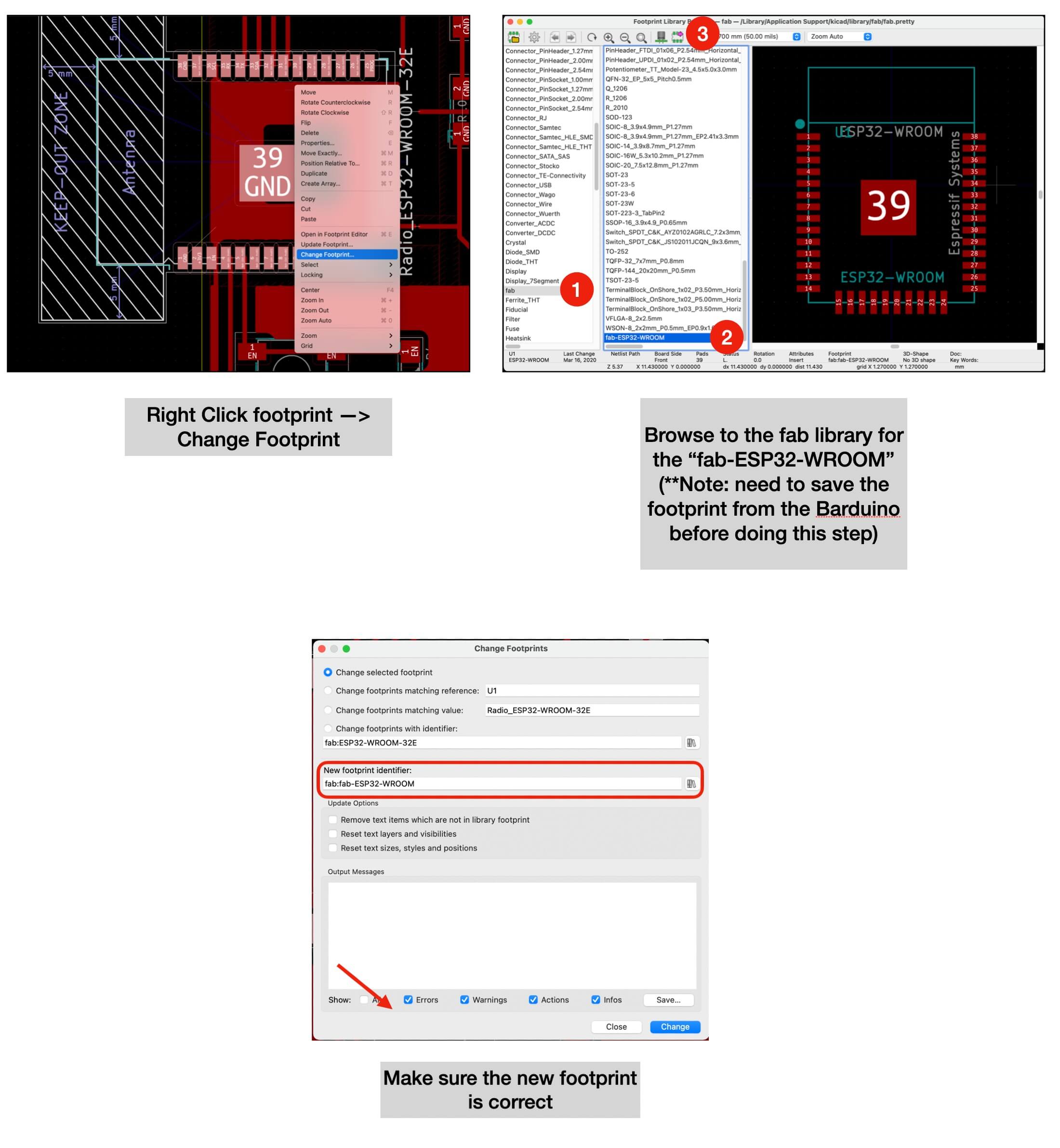
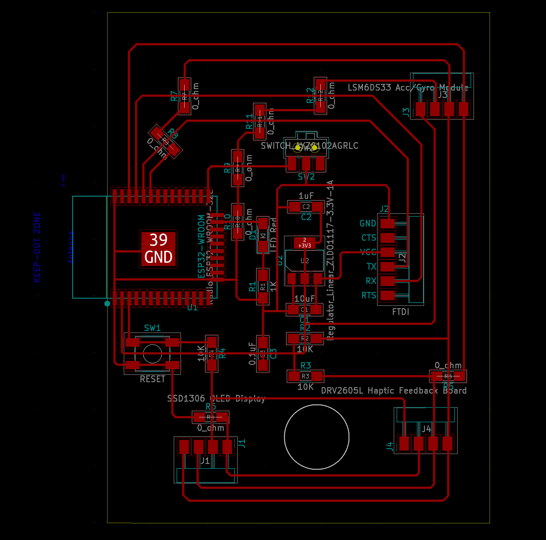
The white/blue components are from Neil's board and I tried to arrange the components in the same way as his board. The purple/black components are the extra ones for my board. The ones without labels are the 0 ohm resistors
May 7, 2021
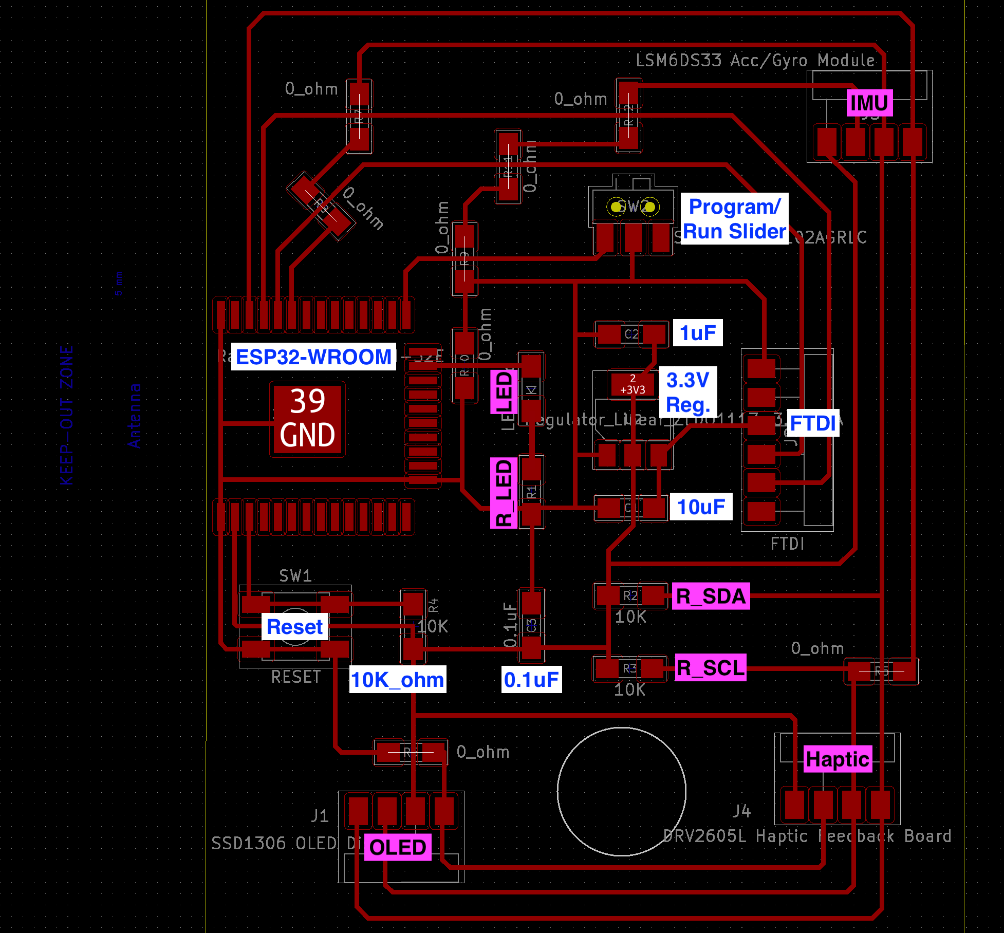
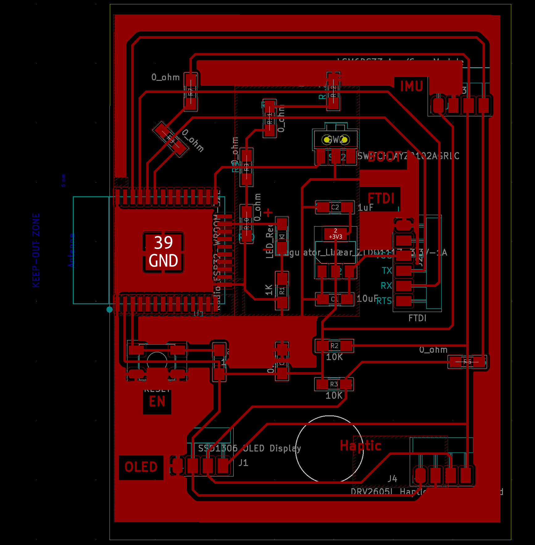
Since I knew that it would take a while to fabricate this board, I decided to spend time making sure my PCB design was correct. I used the built-in "caliper" in KiCad to measure the distances between components to make sure I had left enough room for every component - I found this approach helpful because I realized that I did make a mistake on the OLED display and the Haptic Feedback board. I was able to solve this issue by rotating the OLED board, and also bringing the Haptic Feedback board further away from the resistor. As a result, I was also able to use one fewer 0 ohm resistor. When doing the "ground pour", I blocked out a big area between the FTDI and the ESP32 in order to avoid the FTDI connect directly to the ESP32 without passing the capacitor, since I placed multiple 0 ohm resistor in between. Here are the updated images for the PCB design:
May 10, 2021
Part 1 - Laser cutting attempt
Part 2 - Milling and Soldering
Part 3 - Testing
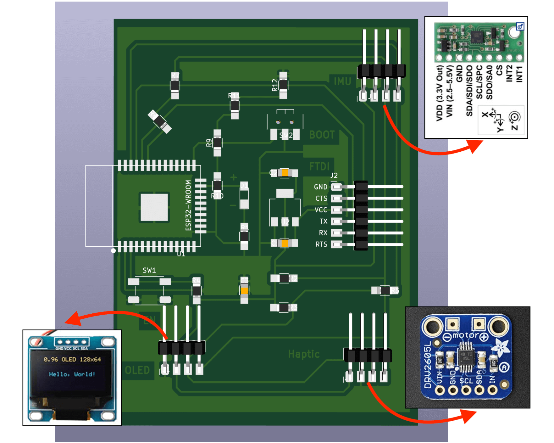
1) Test the Accelerometer/Gyroscope module and OLED display:
2) Test the Haptic Controller module:
Files
Please find below the files that I made for this assignment.
- PCB Design and Production Files:
- Arduino Sketches: