9. Embedded programming
This week’s assignment is related to embedded programming, since it seems to me an interesting topic, I decided to build a new PCB with inputs and outputs (following Neil’s advice) in order to use it in the other assignments.
Assignment
group assignment:
- compare the performance and development workflows for other architectures.
individual assignment:
- read a microcontroller data sheet.
- program your board to do something, with as many different programming languages and programming environments as possible.
Group assignment
What’s the difference between Von-Neumann and Harvard architectures?
These two processor architectures can be classified by how they use memory.
Von-Neumann architecture In a Von-Neumann architecture, the same memory and bus are used to store both data and instructions that run the program. Since you cannot access program memory and data memory simultaneously, the Von Neumann architecture is susceptible to bottlenecks and system performance is affected.

Harvard Architecture The Harvard architecture stores machine instructions and data in separate memory units that are connected by different busses. In this case, there are at least two memory address spaces to work with, so there is a memory register for machine instructions and another memory register for data. Computers designed with the Harvard architecture are able to run a program and access data independently, and therefore simultaneously. Harvard architecture has a strict separation between data and code. Thus, Harvard architecture is more complicated but separate pipelines remove the bottleneck that Von Neumann creates.

The Von Neumann Bottleneck If a Von Neumann machine wants to perform an operation on some data in memory, it has to move the data across the bus into the CPU. When the computation is done, it needs to move outputs of the computation to memory across the same bus. The amount of data the bus can transfer at one time (speed and bandwidth) plays a large part in how fast the Von Neumann architecture can be. The throughput of a computer is related to how false the processors are as well as the rate of data transfer across the bus. The processor can be idle while waiting for a memory fetch, or it can perform something called speculative processing, based on what the processor might next need to do after the current computation is finished (once data is fetched and computations are performed).
The Von Neumann bottleneck occurs when data taken in or out of memory must wait while the current memory operation is completed. That is, if the processor just completed a computation and is ready to perform the next, it has to write the finished computation into memory (which occupies the bus) before it can fetch new data out of memory (which also uses the bus). The Von Neumann bottleneck has increased over time because processors have improved in speed while memory has not progressed as fast. Some techniques to reduce the impact of the bottleneck are to keep memory in cache to minimize data movement, hardware acceleration, and speculative execution. It is interesting to note that speculative execution is the conduit for one of the latest security flaws discovered by Google Project Zero, named Spectre.
Individual assignment
Attiny85 Datasheet
The first thing we must do is carefully read the datasheet provided by the manufacturer Atmel ATtiny25, ATtiny45, ATtiny85 Datasheet, identifying that it match the characteristics we need for our application, in my case I need to identify 3 important parameters:
- Pins: Which will work as inputs or outputs and also which will be used for ISP communication.

- Pwm: Function that will allow me to modulate the signal sent to the led by pulse width and thus be able to regulate the brightness.

- Available memory: For future applications I plan to push the memory of this little microcontroller to the limit so the amount of memory available is very important to me.

And other small things that I also consider important such as the communication protocols that it supports or the libraries available to work with that microcontroller, I consider that it is necessary to read the datasheet of a component that you want to use in order to take advantage of it 100 percent, there is no better feedback than the provided by the same manufacturer.
Manufacturing process
I will not go into much detail in this part because the assignment does not correspond, but I will quickly detail the steps that I followed to finish with a PCB that I can program.
Elaboration of the circuit in EasyEDA

PCB elaboration

Milling procces


Soldering procces

Final result

Programming process
Arduino IDE
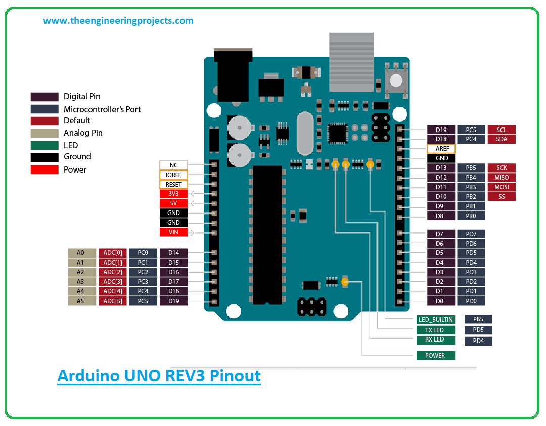
For the programming process I decided to use an Arduino UNO as an ISP programmer because I still have problems entering the laboratory and it was the most available option within my reach. It is curious but it is also recommended to look for the Arduino UNO datasheet to know the pins that this microcontroller uses for ISP communication, once identified it is necessary to wire them with the pins of our PCB as shown below.
D13 to SCK PB2
D12 to MISO PB1
D11 to MOSI PB0
D10 to RST PB5
VCC to 3.3V
GND to GND

We check that all the connections are good and we can connect the USB port to the Arduino and also to the PC to start programming, for that the first thing we are going to do is open the Arduino IDE to load a sketch to the Arduino Uno called “Arduino as ISP ” this is available in the examples tab and is very easy to load.


Then we can start to elaborate our sketch, which will be simple and will use the button and the led integrated in the PCB to blink for a certain number of times when pressing the button.
Source code
const int boton = 3;
const int led = 1;
int buttonState = 0;


void setup() {
  pinMode(led, OUTPUT);
  pinMode(boton, INPUT);
}
void loop() {
  buttonState = digitalRead(boton);   // check if the button is pressed
  if (buttonState == LOW) {
    // turn LED on:
    for (int i = 0; i <= 10; i++) {
      digitalWrite(led, HIGH);
      delay(250);
      digitalWrite(led, LOW);
      delay(250);
    }
  }
  else {
    // turn LED off:
    digitalWrite(led, LOW);
  }
}
Finally we select the parameters of our microcontroller in the Tools tab:
Board: “ATtiny25 / 45/85”
Processor: “ATtiny85”
Clock: “Internal 1 MHz” (can also work at 8 MHz)
Port: “COM6 (Arduino UNO)” (the port assigned to the Arduino)
Programmer: “Arduino as ISP”


Running my code
Once the code is loaded on the PCB, we can proceed to disconnect it from the programmer (Arduino), since the PCB has a CR2032 battery that will allow us to power it independently and we can test that the code is working correctly.

Microchip Studio
Microchip Studio is an Integrated Development Environment (IDE) for developing and debugging AVR® and SAM microcontroller applications. It merges all of the great features and functionality of Atmel Studio into Microchip’s well-supported portfolio of development tools to give you a seamless and easy-to-use environment for writing, building and debugging your applications written in C/C++ or assembly code. Microchip Studio can also import your Arduino® sketches as C++ projects to provide you with a simple transition path from makerspace to marketplace.
You can use Microchip Studio with the debuggers, programmers and development kits that support AVR and SAM devices. Extend your development environment with Microchip Gallery, an online app store for Microchip Studio plug-ins developed by Microchip as well as third-party tool and embedded software vendors.

The first thing we must do is create a project, in this case we will work with C/C++ and the project will be of the GCC C++ Executable Project executable type, then we choose our family of devices (ATtiny85) and we will be ready to start developing our code.


This is a very simple program that makes a LED blink during half second, I will detail some important command lines:
#define LED1_PORT PB1
It defines the port that will be used for the LED, in this case PB1 in our board.
Then we have to setup that port as an output. This is done with the following line of code:
DDRB |= (1 << LED1_PORT);
The DDRB is the data direction for port B. What this does is this, shifts the “1” on left, N-times depending on the LED1_PORT value; and does bitwise “OR” with the value in the port register DDRB. The most important fragment of the code is this, in charge of turning the led on and off
for (;;) {

    PORTB |= (1 << LED1_PORT);

    _delay_ms(200);

    PORTB &= ~(1 << LED1_PORT);

    _delay_ms(400);

}

#include <avr/io.h>

#include <util/delay.h>

#define LED1_PORT PB1

int main(void) {

    DDRB |= (1 << LED1_PORT);

    for(;;) {

        PORTB |= (1 << LED1_PORT);

        _delay_ms(500);

        PORTB &= ~(1 << LED1_PORT);

        _delay_ms(500);

    }

    return (0);

}
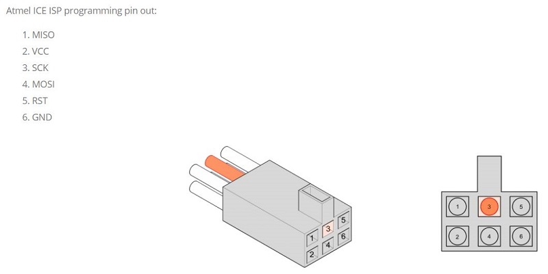
ATMEL Ice Wiring
It is always good to emphasize the correct way how we must connect the programmer cable to our board.

Running my code
Once the code is loaded on the PCB, we can proceed to disconnect it from the programmer (ATMEL ICE), since the PCB has a CR2032 battery that will allow us to power it independently and we can test that the code is working correctly.

You can download the files below:
Week Assessment
During this week, have I :
-
[ ] Linked to the group assignment page ? Yes, I did.
-
[ ] Documented what I’ve learned from reading a microcontroller datasheet ? Yes, have a look at Attiny85 Datasheet.
-
[ ] Programmed my board ? Yep.
-
[ ] Described the programming process I used? I tried to be as clear as possible so that others can replicate my work.
-
[ ] Included my source code ? Yes, have a look at Source code.
-
[ ] Included a short ‘hero video’ of my board ? It was necessary to document that long-awaited and satisfying moment.