7. Electronics design
This week’s assignment focuses on electronic design, since we must understand the operation of the test equipment available in the laboratory to check the correct operation of our boards, the other assignment is to create a circuit called ECHO HELLOW-WORLD with some extra components like LED’s, buttons, etc. For that we must choose which microcontroller we are going to work with and the most important thing is to read the datasheet to understand its characteristics.
Assignment
group assignment:
- use the test equipment in your lab to observe the operation of a microcontroller circuit board.
individual assignment:
- redraw an echo hello-world board, add (at least) a button and LED (with current-limiting resistor) check the design rules, make it, and test it extra credit: simulate its operation
Group assignment
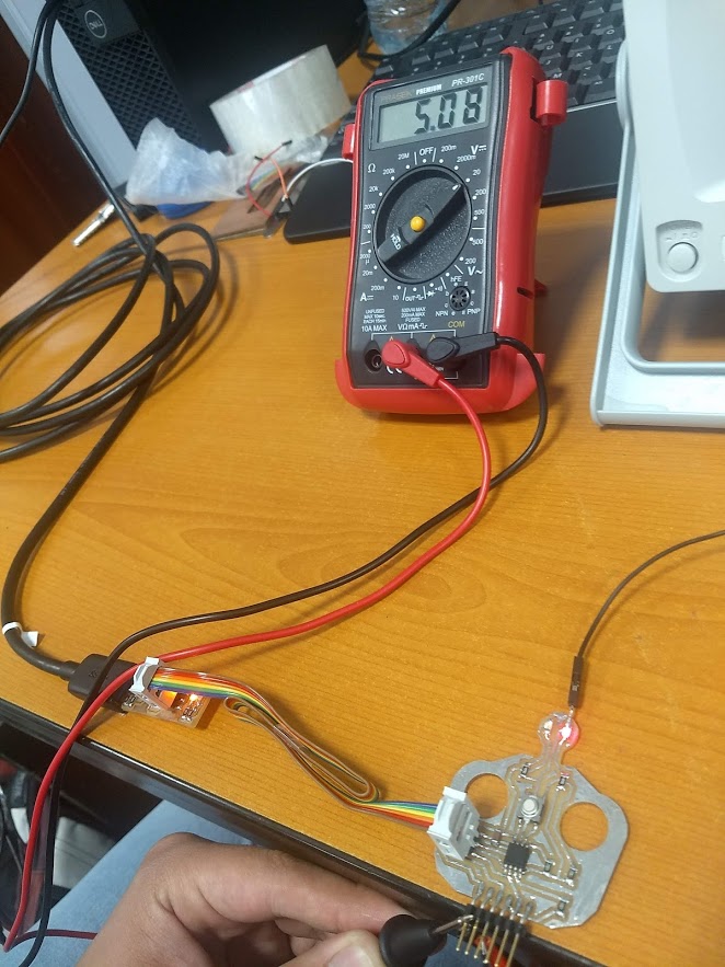
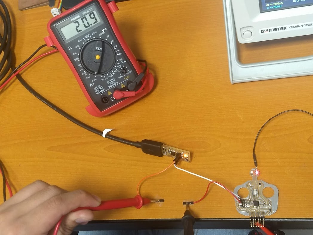
This assignment was done after implementing the individual assignment board, since the laboratory test equipment is indicated to debug a board and to be able to accurately identify any problem. The first tests were made with the multimeter, this device allows us to measure voltage, current and continuity. As we are connected to the USB port of the PC, we must check that the voltage is 5V, the current consumption should be around 20mA and there should be no continuity between 5V and GND.
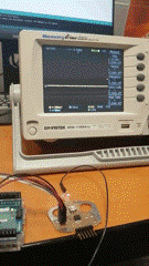
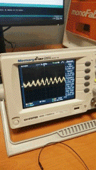
Next we are going to use the oscilloscope, an oscilloscope is an electronic display instrument for the graphic representation of electrical signals that can vary over time. The signals that we are interested in verifying are the PWM pulses and the information that travels from the PC to the board when loading a program.
Individual assignment
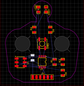
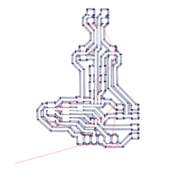
To do this job I had have modified the original board design, incorporating two leds (blue and red) and a button, besides to personalize this job, I decided modify the design form at structure adopting a robot head shape however in the process to accommodate the routs and components I had have to adjust the shape and I hope that you can recognize as that. la design to incorporate Modificado 2 characteristics led and button
PCB fabrication
To make this task I decided to use the Attiny85 and modify the design of the FabtinyISP to add 2 LEDs and a button, I also decided to give it a creative touch and make the board from the shape of a robot’s head and most importantly I added an FTDI connection thinking on the assignments to come in the next few weeks.
For PCB design I generally use EagleCad, but constantly looking for libraries for components is a bit tedious, so I decided to use an online tool from a PCB manufacturer called JLCPCB the name of the tool is EASYEDA, maybe it is a bit limited but the advantage is that it has a wide library of components which will allow me to work in a more fluid way, since this board is simple I think it is the right tool for the job.
I followed this tutorial EasyEDA Tutorial provided by the same manufacturer and it was not complicated at all, it should be noted that I have previous experience designing in EagleCAD and migrating to this software was very easy, for all PCB manufacturing processes we have to follow the same steps, first create a schematic circuit with all the components that we are going to use and then we start to make the board.
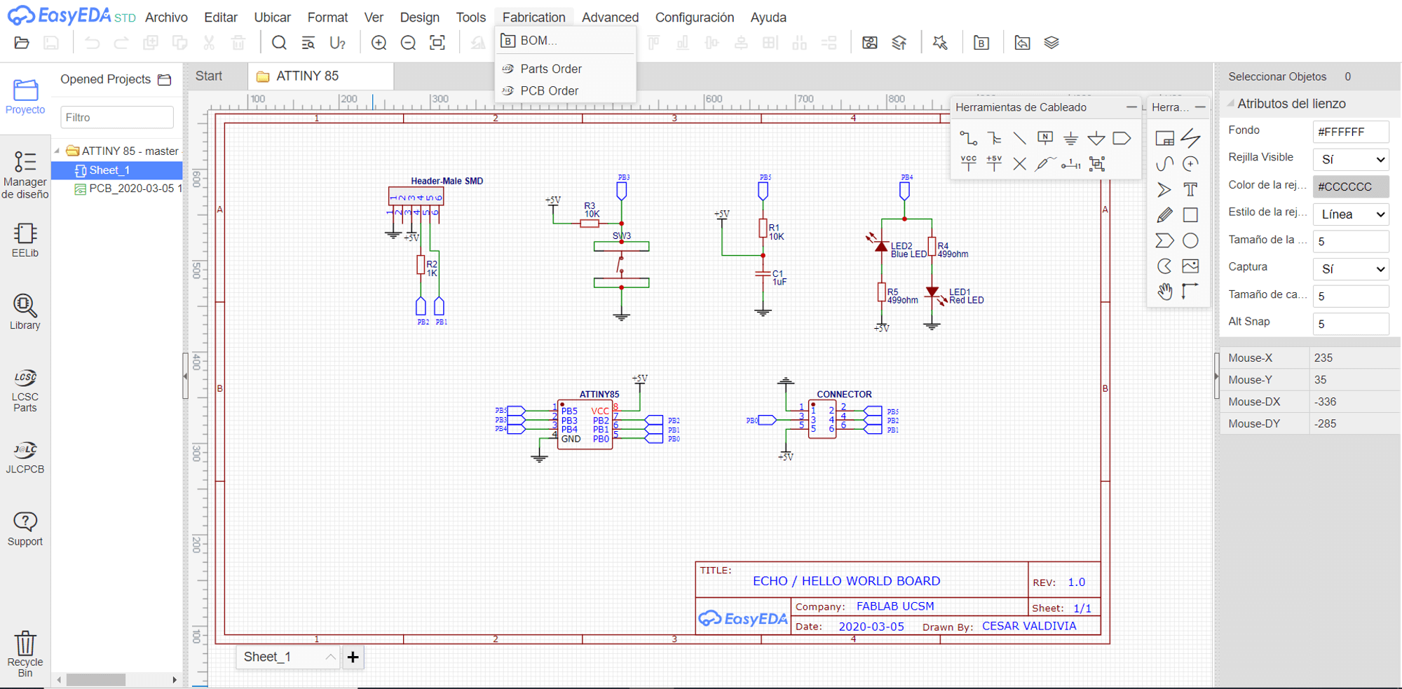
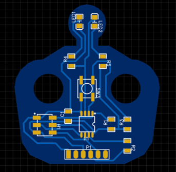
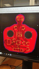
With the schematic already created and all the connections checked, we can go on to elaborate the shape of the board and then add the components in the desired position and the most important thing route all the tracks, I think the part that took the most of the time was elaborating the shape of the board, due to its symmetry and also had to think about the spaces where the tracks should be placed.
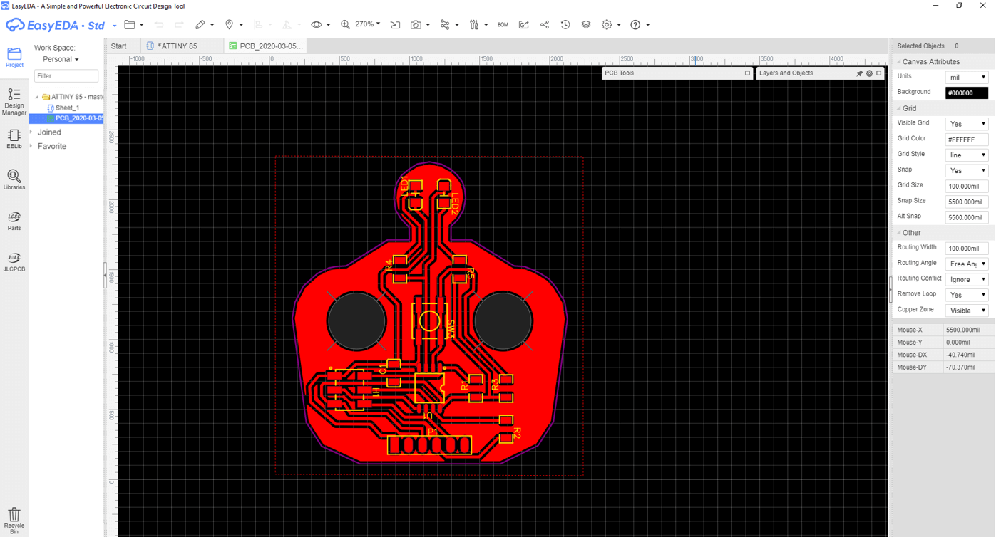
Then we have to export the traces and the outline as PNG and then enter them into Fabmodules to be able to process them in our Monofab, repeating the same steps that we did in the week of electronics production.
Manufacturing problems
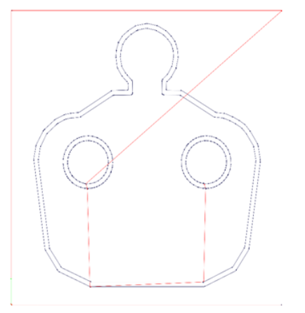
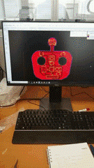
Something that I did not mention was that the first design of the board was slightly different, but at the time of milling the clearance destined for the traces were very tight and there were also other parts that need to be reinforced, so really all the design that you are seeing is actually the version 2, I am attaching a small gif of the moment when we were milling the version 1 board. As you can see, the robot’s head was square shaped and the antenna was thinner. It was also necessary to perform a post-processing with the cutter because some traces were too close, but nothing difficult to solve with a little bit of patience.
Version 1:
Version 2:
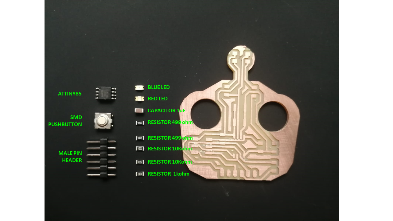
Materials used
- Attiny85
- SMD Pushbutton
- Male pin header
- Blue LED
- Red LED
- Capacitor 1uF
- 499 ohm resistors
- 10Kohm resistors
- 1Kohm resistor
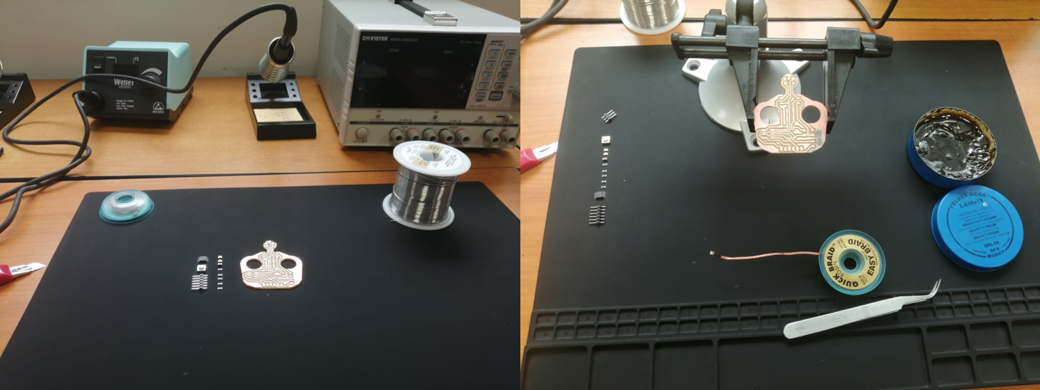
With the board already processed, the next step is to weld all the components, the first thing we must do as good practice is to set up our entire work area, the soldering iron, the fan and the solder paste, additionally you can use solder wick, to facilitate the soldering of the pieces and also to establish an extra layer of protection, I decided to cover all the copper with a thin layer of tin that will also allow me to solder the components in an easier way.
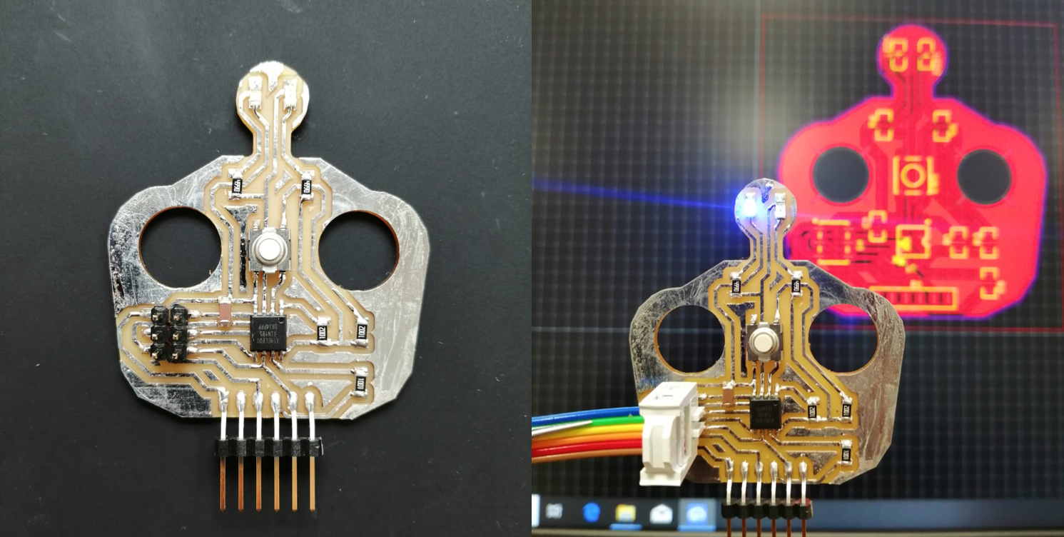
Finally, we soldered all the components and as shown in the group assignment, all the tests were performed on the board to verify that it was working correctly, a code was loaded to regulate the intensity of the 2 LEDs using the pulse width modulation PWM and that showed that the board was working perfectly.
You can download the EasyEda file and the code below:
Week Assessment
During this week, have I :
-
[ ] Linked to the group assignment page ? Yes, I did.
-
[ ] Documented what I’ve learned in electronic design ? Yes, the elaboration of electronic circuits is not learned overnight but the tools are increasingly more intuitive and help us to perform the tasks with the least effort, there will be always a tutorial on YouTube to help us understand a tool that we do not know how to use.
-
[ ] Explained problems and how I fixed them ? Yes I did, maybe the shape changed a little bit, but this assignment helped me understand some things that I should take into consideration when designing and milling boards.
-
[ ] Included my original design files (EasyEDA) ? I did, I hope they are useful for other people or maybe they can improve them.
-
[ ] Included hero shots of my board ? I took as many photos as possible as I am very satisfied with the end result.
-
[ ] Loaded a program and tested in my board ? Yes, have a look at the Group Assignment