5. Electronics production
This week’s assignment introduces us to the world of electronic production, starting with the development of an electronic circuit that later will help us to program our boards, I find it very interesting since I have a little experience soldering electronic components, I will find out how it goes with the SMD components since I generally welded thru-hole, I am pleased to test the functions of the milling machine that we have in the laboratory (Roland SRM-20).
Assignment
group assignment:
- characterize the design rules for your PCB production process.
individual assignment:
- make an in-circuit programmer by milling and stuffing the PCB, test it, then optionally try other PCB processes.
Group assignment
Before starting with the individual assignment, it is necessary to characterize our milling machine, this will help us to make the most of the machine for the jobs we do later.
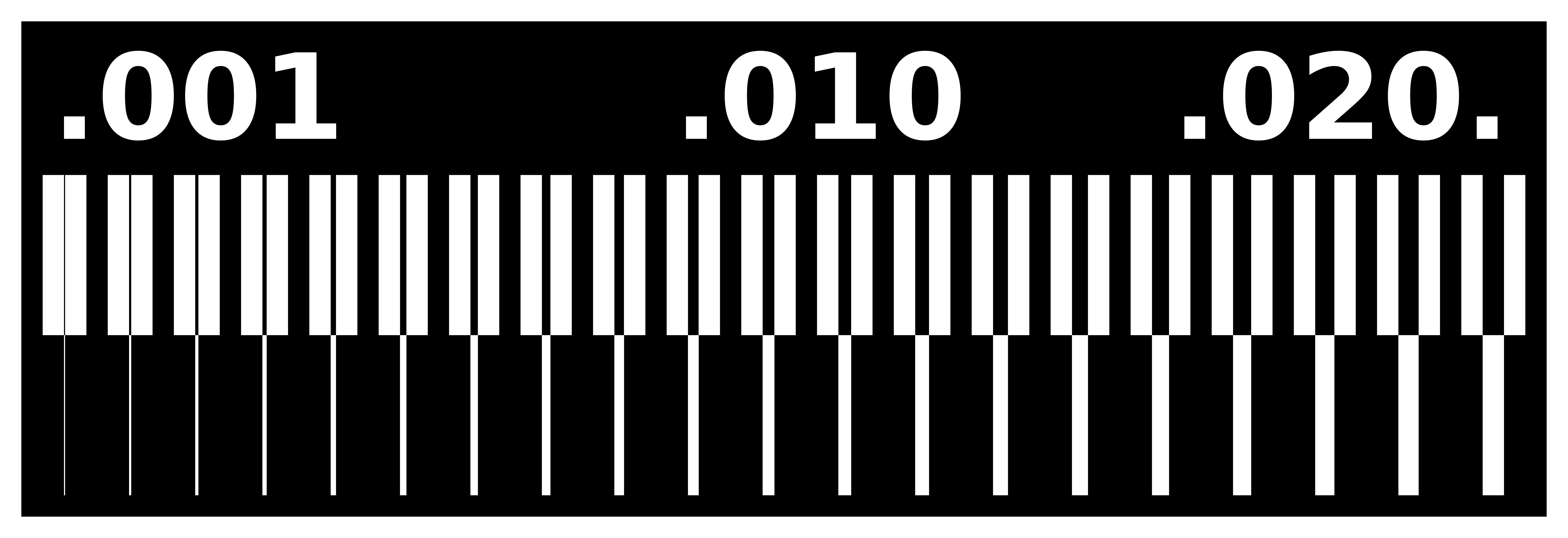
Since the task consists of milling a PCB, we must identify the resolution that the Roland SRM-20 gives us, with that information we can determine the minimum thickness of the traces to elaborate our in-circuit programmer.
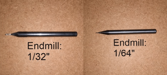
For this characterization I decided to use 2 endmills 1/32 and 1/64 since they are the only ones that we currently have available, I think they will be enough to adequately perform the task, the 1/64 will allow us to elaborate all the tracks and the other one of 1/32 will be used to cut the edge of the board.
The first step is to download the files to start the milling process, I will use the images available in the electronic production session Traces and Interior

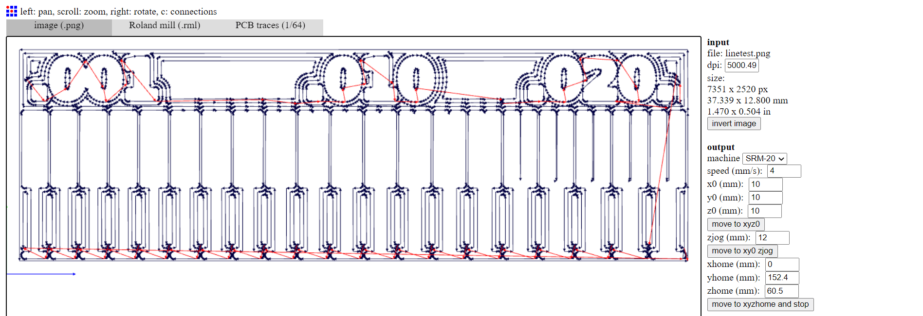
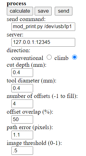
For this characterization I decided to use Fabmodules as it allows me to transform my .png images into files that I can upload directly to the machine, the steps are relatively simple:
-
Download the TRACES and INTERIOR files as .png.
-
Open http://fabmodules.org/ in the internet explorer.
-
Select the option image(.png).
-
We select the type of output format that we are going to generate, in this case Roland mill (.rml).
-
We define the process, in this case will be PCB traces (1/64).
-
We select extra parameters to generate the file, such as the machine (SRM-20), speed, home, etc.
-
We click on CALCULATE process.
-
Finally we save the file by selecting SAVE.
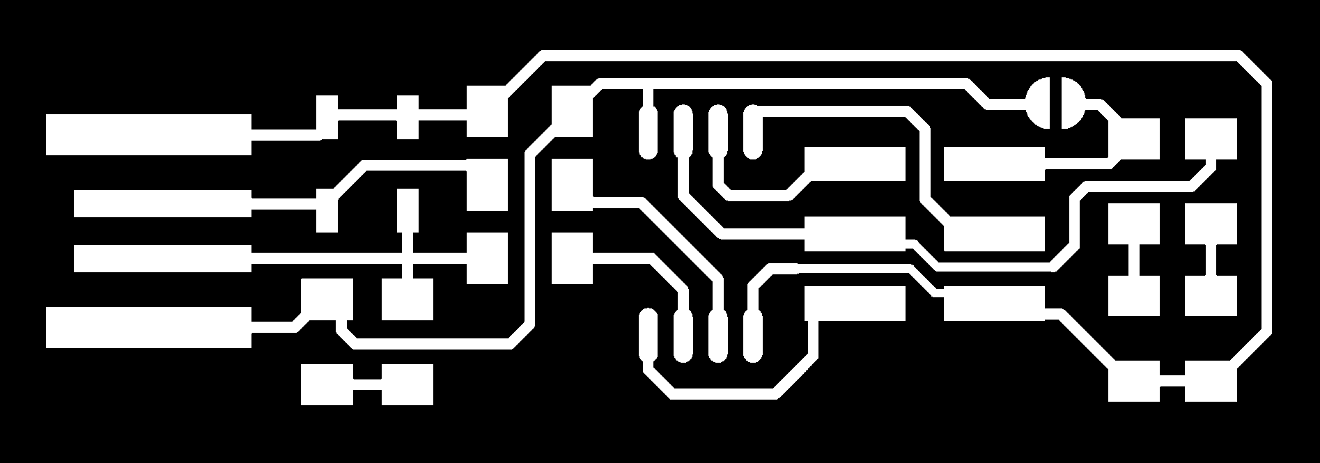
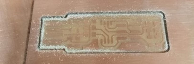
Here we can see the work of the finished 1/64 milling cutter, now it only remains to carry out the same process as previously detailed to cut the edge with the 1/32 mill.
As you can see in the image we add a sacrificial layer made up of another PCB in order to avoid damaging the endmill when we miscalculate the depth of the trace.
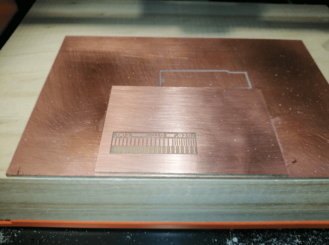
With that piece made we can already identify the resolution of our machine, because we are using an endmill of 1/64 the maximum resolution that we can achieve is 0.010, an acceptable value for the elaboration of our board.
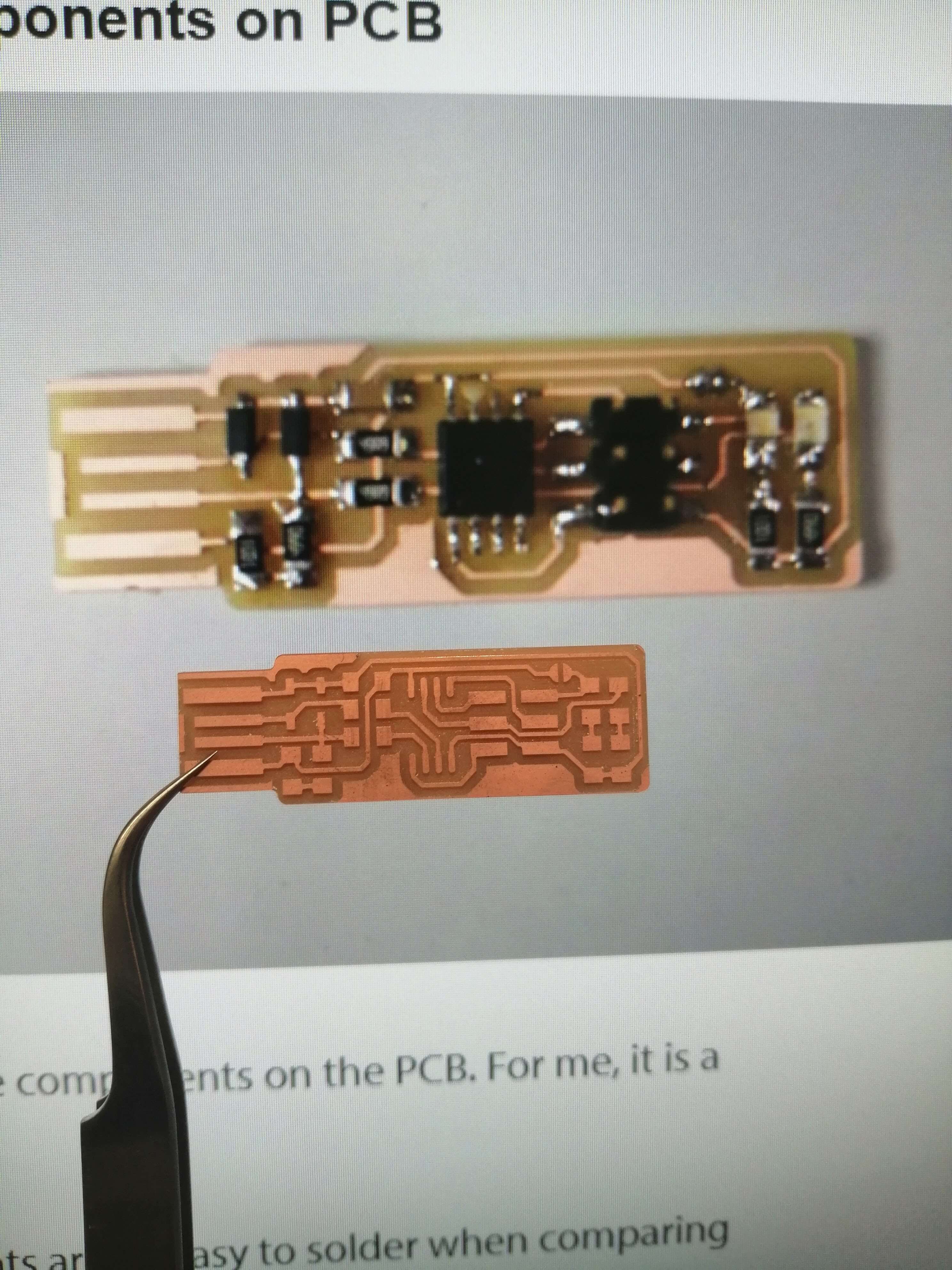
In-circuit programmer fabrication proccess
I am going to detail all the necessary steps to finish with a fully functional board, I must admit that it was a process that required many tests, but I am very satisfied with the result, I had problems with some parts, but I managed to solve them and I hope that this information also help other people who want to implement the same board.
The board I decided to implement was the FabtinyISP because I consider the ATtiny85 to be a microcontroller with a lot of potential, now I am a lover of the ATtiny402, but we will talk about that later.
The first thing we need to do is find the .png files for the Traces and the Cut, so that we can process those images on the fabmodules page.

The steps required to process the PCB are the same as those used in the group assignment:
-
Download the TRACES and CUT files as .png.
-
Open http://fabmodules.org/ in the internet explorer.
-
Select the option image(.png).
-
We select the type of output format that we are going to generate, in this case Roland mill (.rml).
-
We define the process, in this case will be PCB traces (1/64) for the traces and PCB outlines (1/32) for the cut.
-
We select extra parameters to generate the file, such as the machine (SRM-20), speed, home, etc.
-
We click on CALCULATE process.
-
Finally we save the file by selecting SAVE.
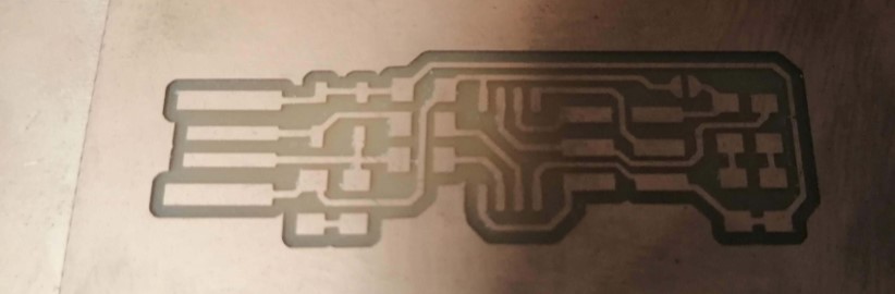
We will end up with 2 files that we are going to upload to our machine to start cutting, I was so excited that I forgot to document the process of uploading the file, but it is simple and the most important thing is to define the value of Z to be able to perform the milling process, otherwise if it is too deep we will end up damaging the PCB or perform a ghost cut.
Once all this is defined, we hit the start button and we begin to see the mesmerizing milling process, as long as the PCB does not move from its place, in my case I used double sided tape to hold the PCB and it worked wonderfully.
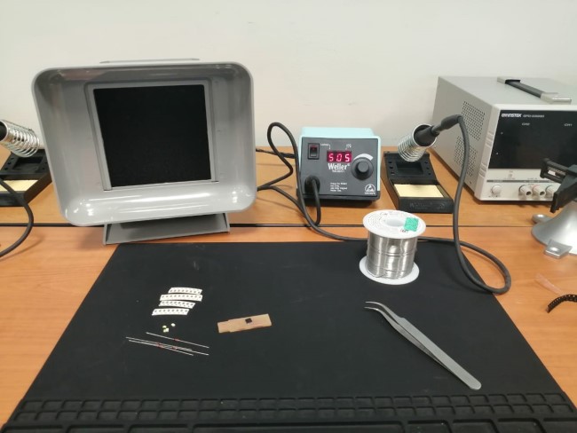
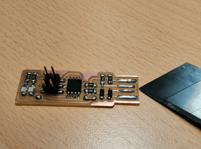
I am excited to be closer and closer to the final result, now comes the funniest part which is soldering all the necessary components for the board
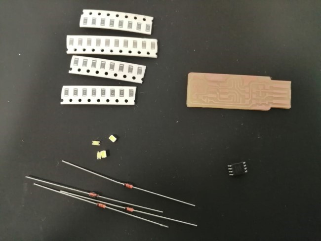
Today most electronic components are only made with surface mount packages (SMD), these packages are usually significantly smaller than through hole component (THT) packages. So at first glance for a person who has no experience in soldering it may seem difficult to work with SMD due to its small size, but it is not like that, with the right tools and a little bit of practice soldering SMD components is much easier and faster than welding THT (through hole technology) components.
Components list
- 1 x ATtiny85 microcontroller (SOIC package)
- 2 x 499Ω resistor
- 2 x 49Ω resistor
- 2 x 1KΩ resistor
- 2 x 3.3v Zener diode
- 1 x 0.1mf capacitor
- 1 x Red led
- 1 x Green led
- 1 x 2x3 Male header pins (smd)
- 1 x 20cm 6wire Ribbon cable
- 2 x 2x3 Female Header IDC Ribbon Cable Transition Connector
- 1x 4cm x 8cm FR4 Copper Clad
In the welding process we have a visual feedback where we can observe how the heat flows between the welder and the component. If we put the soldering iron on the component pad and when we put the tin we see that it is difficult to melt, or it melts very slowly, it means that we need to increase the temperature of the station (or put a larger tip). If, on the other hand, if when we put the soldering iron we observe that the tin melts very quickly (something observable with practice), or even that the component with other pads soldered to the PCB moves, because we are getting too hot.
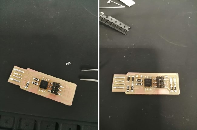
Depending on the number of offsets you milled, there might be a tiny bit of copper left at the edge of the board in front of the USB contacts. 5 offsets should be sufficient to remove all of the copper in the milling process, but takes a bit longer to mill. If you milled fewer offsets (I did 3 in the above photo), the extra copper can be removed with a knife. Only the copper in front of the pads needs to be removed; the copper left on the sides is fine.
While it may seem early to start debugging already (we haven’t even tried anything yet!) it is always prudent to check your work before plugging in a board. It only takes a couple of minutes and can save you headaches down the road.
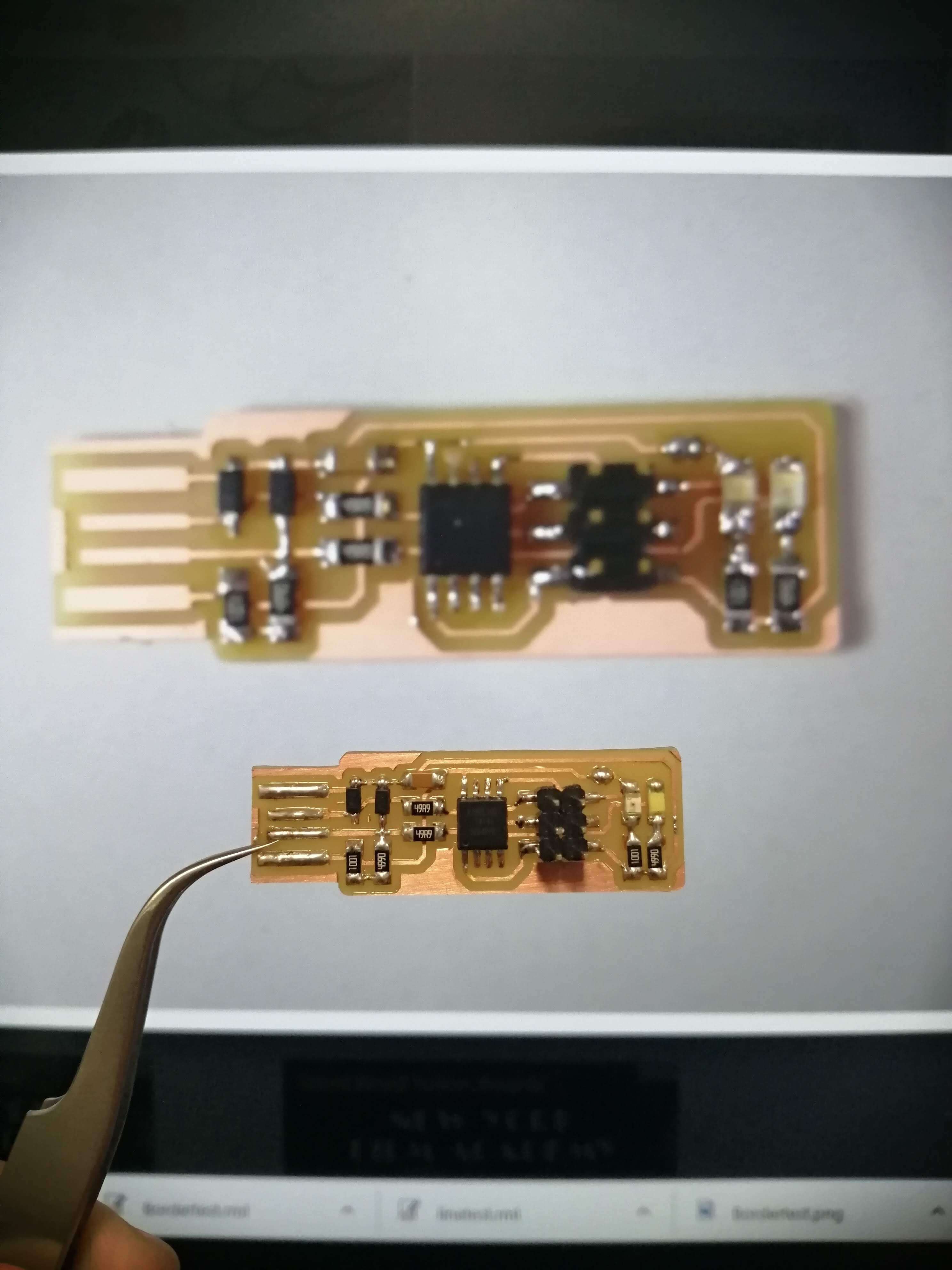
Check your board against the schematic and PCB layout image to make sure that you have installed the correct components in the correct locations and orientations. Inspect your board visually. Components should be flat on the board, not tilted with pins in the air. Solder connections should be smooth, and solder should have flowed both onto the pin and onto the pad. If you still see a lot of exposed copper on the pad, or the solder is lumpy and draws up into a point where you removed the iron, you probably don’t have a good connection. Reflow by applying heat and flux (either from a flux pen or by adding a tiny bit more solder). Also look for unwanted solder bridges between nearby traces and pins. Use a multimeter to check for shorts between VCC and GND.
Continue through the entire programming process detailed here Using the GNU AVR toolchain on Windows 10
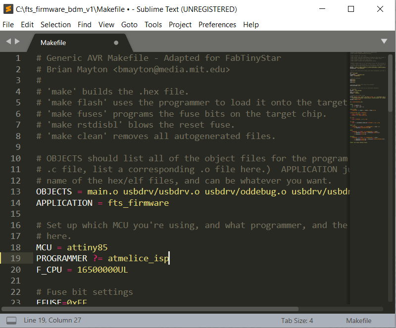
Everything went as expected without the need to use Zading as the Atmel programmers were automatically installed together with Atmel Studio as the tutorial indicates (but that didn’t really happen), I was having problems when loading the .hex file to the board, then I realized that I had to indicate the programmer I was using in the Makefile.h file, using an editor like Sublime I was able to edit that line of code with the correct name from the programmer I am using a White box with blue stripe: atmelice_isp.
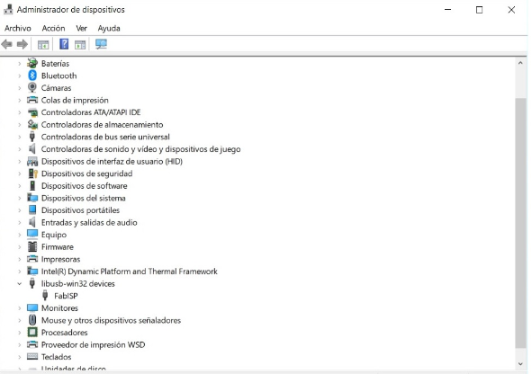
Libusb brought me many problems and also Atmelice, luckily I realized that I was not the only one with that problem and I found a post on internet that solves it (everything would have been easier if I worked it in Linux), carried out all the steps and using Zading modify parameters so that my programmer is recognized by AVR dude and can run the Make flash command. Atmel ICE with AVRDUDE, cannot find device
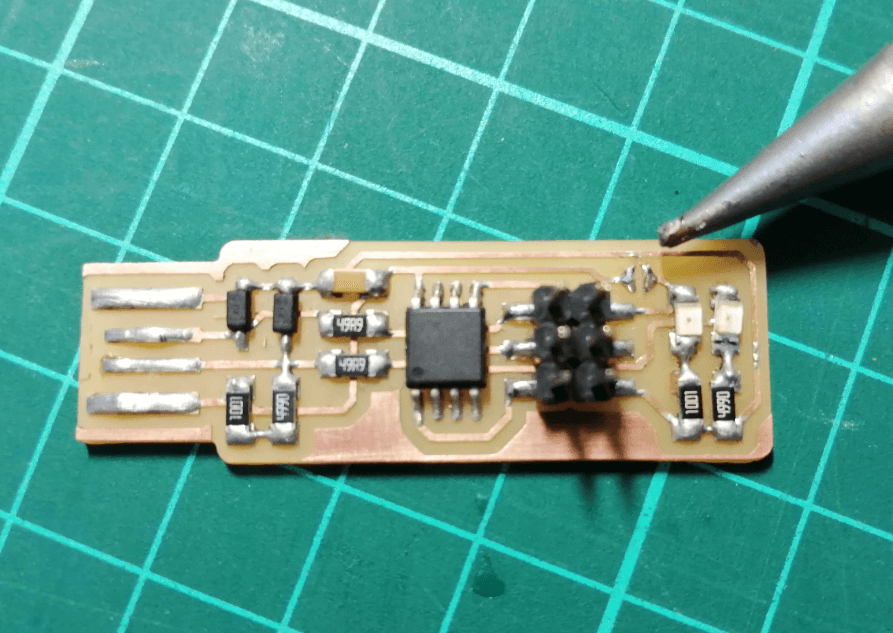
Then I ran the make fuses command. I made sure before resetting the fuses that my card was recognized by the PC
That will set up all of the fuses except the one that disables the reset pin. Finally I unsolder the jumper and my board was ready to program.
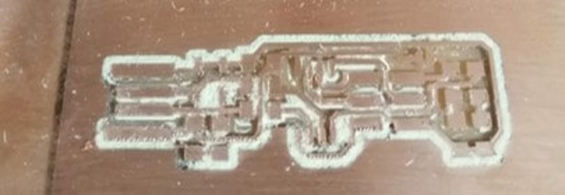
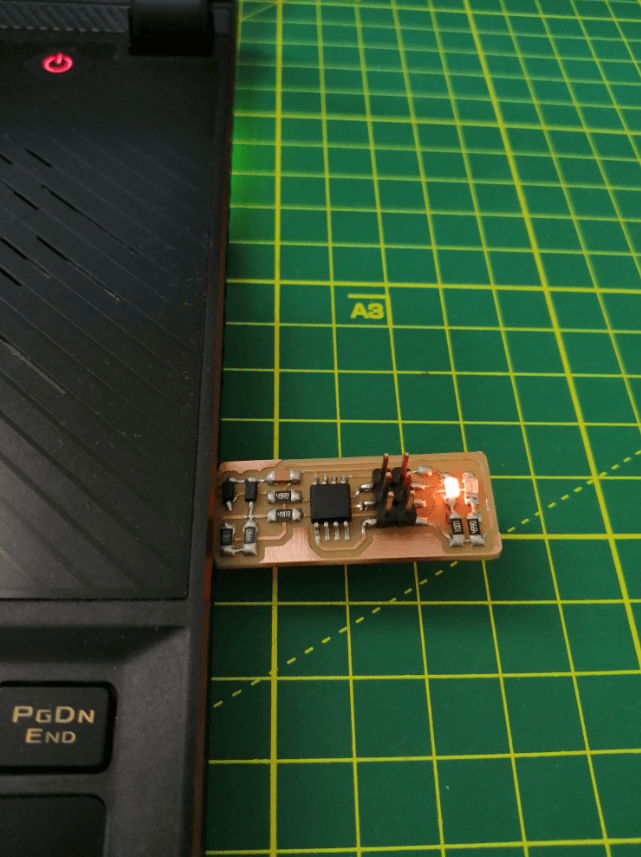
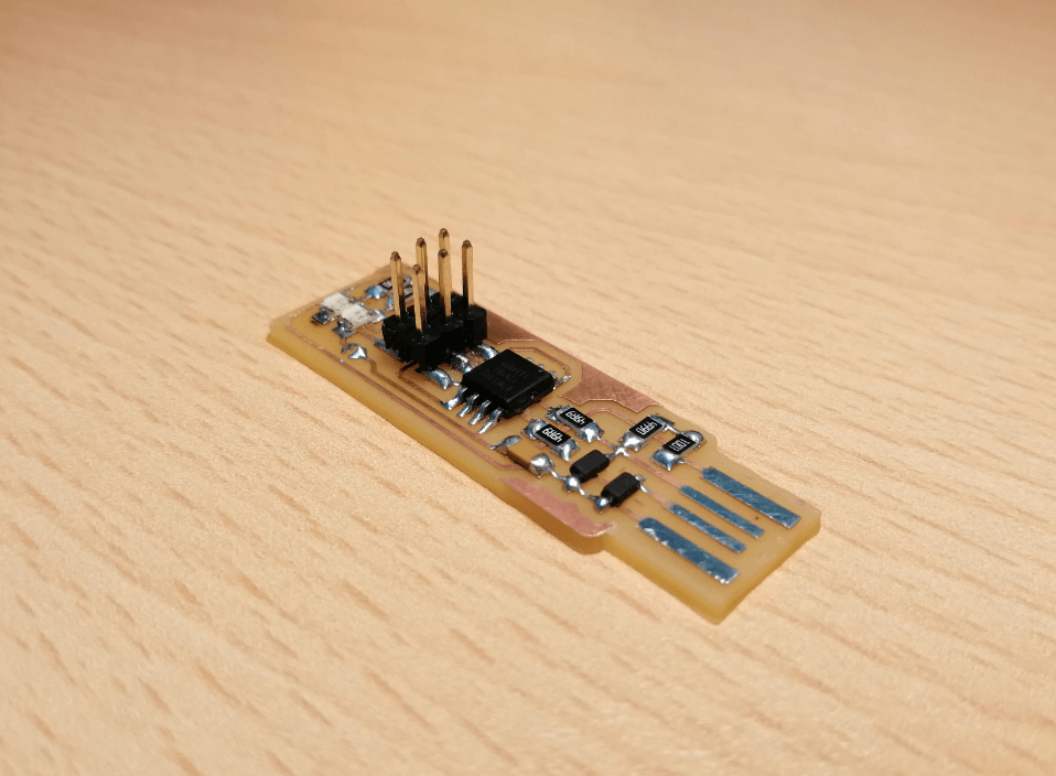
As a conclusion I must indicate that all the tasks were completed with enough time, but I am left with the desire to try to make a flexible circuit board using the vinyl cutter. I consider that the part that demanded the most of this assignment was programming the board, at the beginning I was trying to do everything directly, connected the FabTinyISP directly to the PC and did not see any results, then I realized that it was necessary to use a programmer to program my board, maybe that error was what consumed the most of my time, but then everything went as I expected. I reattach the image of my finished board because I am excited to think that I was able to do this job.
Week Assessment
During this week, have I :
-
[ ] Linked to the group assignment page ? Yes, I did.
-
[ ] Documented how I made (mill, stuff, solder) the board ? Yes, have a look at the In-circuit programmer fabrication proccess.
-
[ ] Documented that my board is functional ? I followed all the steps on the FabtinyISP page and used extra resources so that my board works correctly.
-
[ ] Explained any problems and how I fixed them ? Yes, some of them during manufacturing process and others during programming.
-
[ ] Included hero shots of my board ? I took as many photos as possible as I am very satisfied with the end result.