7. Electronics design
Group Assignment
I was away from Waag this week because I flew back to Miami for a family wedding. I was not able to participate in the group assignmnet, but reviewed my classmate’s work. Here is the link:
Weekly Assignment
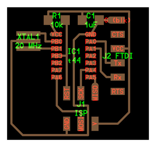
This week, I worked on the echo helloworld Tiny44 board that Neil went over in the video.
As I was away this week, I learned to use KiCad by watching Neil’s lecture on electronics design from 2019 and from looking at previous students’ pages.
First, I downloaded KiCad
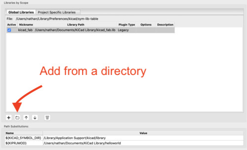
Next, I downloaded a library to work with from the FabAcademy github.
Then, I opened Kicad and loaded the library into it. The Library I used is kicad_fab.
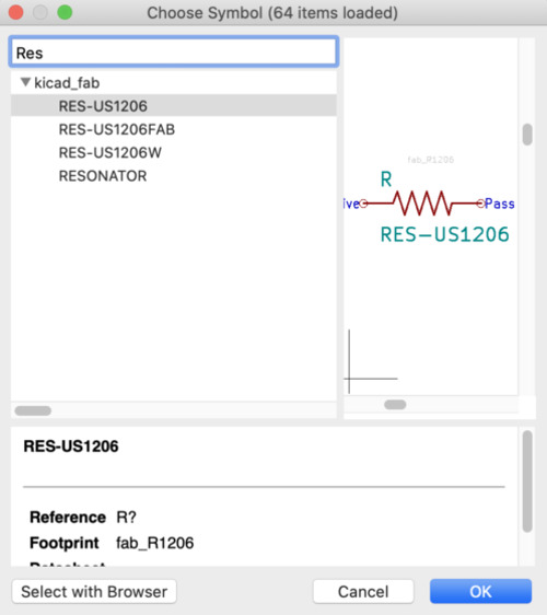
After the library was setup, I began to draw my schematic. At first, I thought I should be using the icon at the top that looks the same as the add component button button on the right panel and got a bit confused. It turns out tis is part of the commands for editing the library. Here are the main controls I used in the schematic editor:
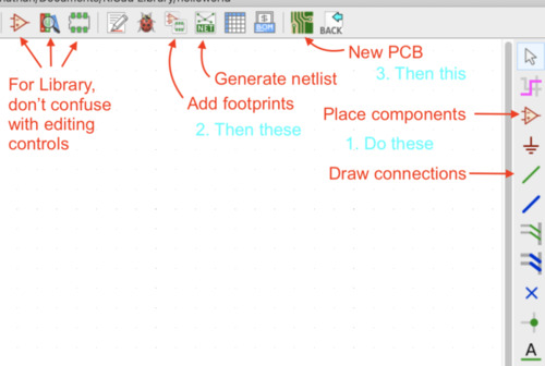
I clicked on the icon to place components and populated my schematic with parts. I found this search/placement easy. The only times I ran into trouble were first, with knowing which symbols to choose out of multiple options, but after rewatching Neil’s video from 2019 I found him saying we use 1206 parts. Additionally, some parts I would have to try to search for in multiple ways. For example “button” did not return results, while “switch” did. Also helpful- some parts would be listed twice, with SMD after one of the listings. This stands for surface mount design, so we choose these!
After everything was placed, I then clicked on the green wire icon and drew connections between everything based on the image. It felt wrong to cross connections, but bridges are represented by a dot at the intersection, so scrossed lines are fine in the schematic.
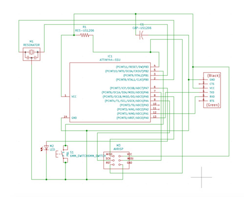
However, after returning to Waag, one of my classmates showed me that they had learned in the local lesson to draw the connections to shorthand symbols for Vcc, Ground, and other components so that overlapping lines don’t actually have to be drawn. Next time I design a board, I will do this.

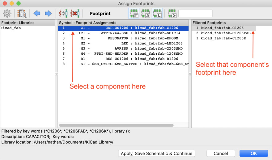
First, click on the above left icon to choose footprints, and next the following icon to generate netlists. The footprint dialog works like this:
Now, I opened the PCB editor and clicked on load netlist and update PCB from schematic:
After that, I had the rats nest loaded.
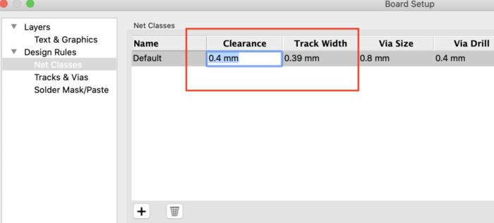
Before drawing the PCB, I set the design rules by going to File > Board setup > Design Rules > Net classes. For our machine, Henk recommended we set the clearance to .4mm and track width to .39mm. These settings limit the size and proximity of the copper pathways in the design to make sure the drillbit in your machine will be able to handle the design.
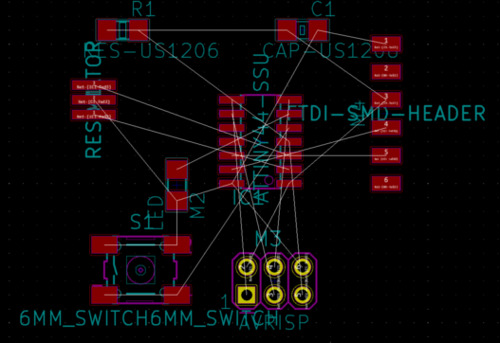
Now time to make the design. These are my components after dragging them apart from the initial rat’s nest:
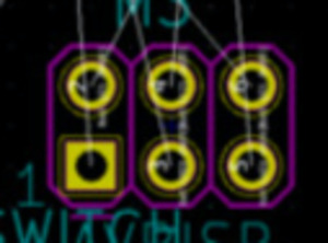
After this, drawing the traces was pretty straightforward, as I tried to mostly follow the layout from the image of Neil’s board on the fabacademy website. I started with the ground line, but ran into trouble when I couldn’t run it underneath the ISP header. I asked Henk what the issue was, and he said I had chosen the wrong footprint for the ISP.
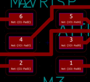
I went back into the Schematic editor and changed the footprint from 2X03 to 2X03SMD. I again clicked generate netlist. In the PCB editor, I clicked on load netlist and update PCB from schematic. It asked me if I was sure and I clicked OK. After that, nothing changed. I deleted the old footprint for the ISP, and then the new one appeared.
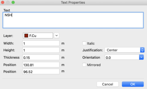
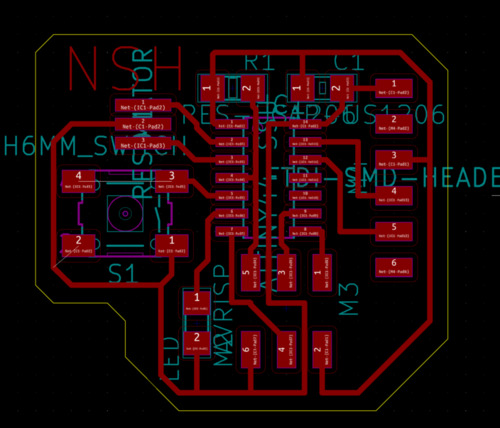
After that, I was able to draw the whole path. I additionally added my name using the Text tool, represented by the ‘T’ icon.
Before exporting, you can check the design rules again by clicking on the Ladybug icon at the top of the screen.
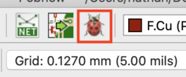
This brings up a window where you can run a design rules check again based on any rules you set in the setup. You can also change the values of the test if you want to see if the design will fit within other parameters.
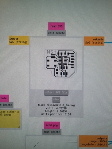
Finally, I clicked File > Export as SVG. I saved these files, loaded them onto a USB, and brought them to the computer with the milling machine.
This was my first time opening an SVG in mods. The only difference from milling with PNGs in previous weeks is that I had to invert the colors in the image in one of the windows.
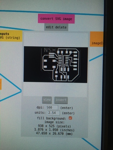
I used the mill traces settings, set the origin, adjusted Z axis, and sent the file.
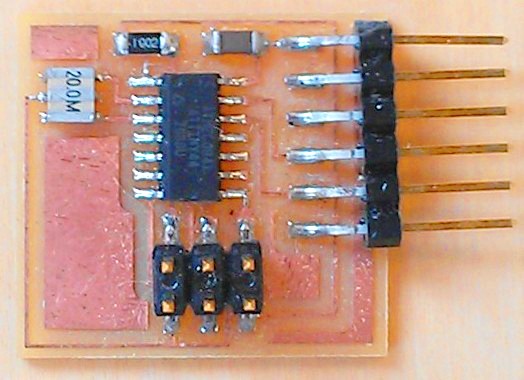
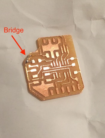
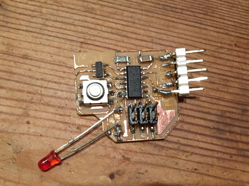
The design milled successfully. I then vacuumed the dust, changed the drillbit, and loaded the outline file. The preview did not show the 3D path for the bit. In retrospect, this might be because I was starting with an SVG. To compensate, I set the offset to 4. I am not sure why I did this… it doesn’t really make sense. In the end, this did work to cut my board, but it made the path too wide and removed a bit of the ground trace. Additionally, the drillbit I used for the traces seems to not have been in great shape. I ended up with a kind of rough board. I considered scrapping it and starting the next day, but decided to test it with the multimeter. I didn’t have confidence because the paths looked so rough. It turns out all the connections worked except for the ground! I decided to stick with this board, and patch that path with a bit of wire. I soldered some wire to make a bridge across the part of the ground that was removed and tested with the multimeter. It worked as well!
I then stuffed the whole board and tested it with the multimeter. All seemed ok… but before connecting it to my computer I looked at Rinke’s board to compare. I noticed he had more resistors than me and I immediately saw a problem-I did not use a resistor for my LED on my board. This is what happens when I miss the local lesson! However, after looking at my board I thought I could probably squeeze in the resistor on the copper trace leading to the LED.
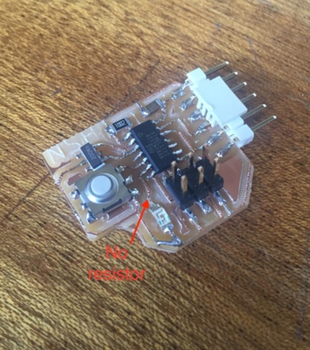
There ended up being enough room and it was not too difficult to attach the resistor.
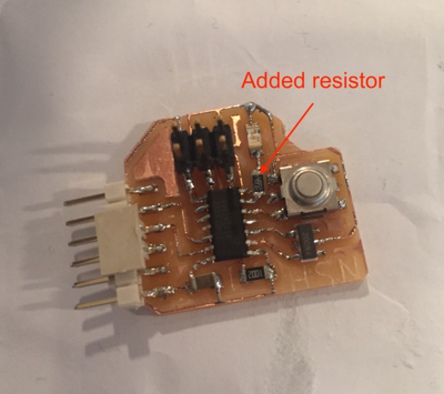
I tested all of the connections with the multimeter and it still seemed to work well.
Note on pull up/pulldown
After global review, it was noted that my button did not have a pull up or pull down resistor. This may have affected its performance and have been the reason why i was not able to get a program to work with it in later tests.
In my design I simply have my button connected between the pin on the board and GND. This means my button is “floating”. I assumed, with this design, that the pin would normally be HIGH as the microcontroller was powered, and that when the button was pressed and the pin connected to the GND that current would then leave the pin and it would become low. This is likely not the case, and to ensure that the button moved the pin from high to low, I should have used a pull-up resistor. This works by connecting the pin to the VCC line with a resistor, to ensure that this pin is reading near the VCC power and therefore high. When the button is pressed, this power then runs into the GND line and the reading changes to low. This ensures variance in readings on the pin. The resistor additionally prevents the button from directly connecting the VCC and GND lines, which would cause a short.
More can be read about pull-up/pull-down resistors here.
Programming
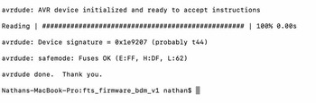
Next, I connected it to my TinyISP, with that connected to the computer, and ran
avrdude -c usbtiny -p t44
The computer found my new board!
Now, time to try to run Blink.
I downloaded arduino, and followed the instructions from Andrew Sleigh’s fabacademy page to get it set up for the tiny44.
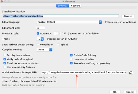
I went into the Preferences window on arduino by going to Arduino > Preferences in the menu bar.
In this window, there is an “additional boards managers” URL dialog. In this field, I added the following link, which I sourced from Andrew Sleigh’s guide above: https://raw.githubusercontent.com/damellis/attiny/ide-1.6.x-boards-manager/package_damellis_attiny_index.json
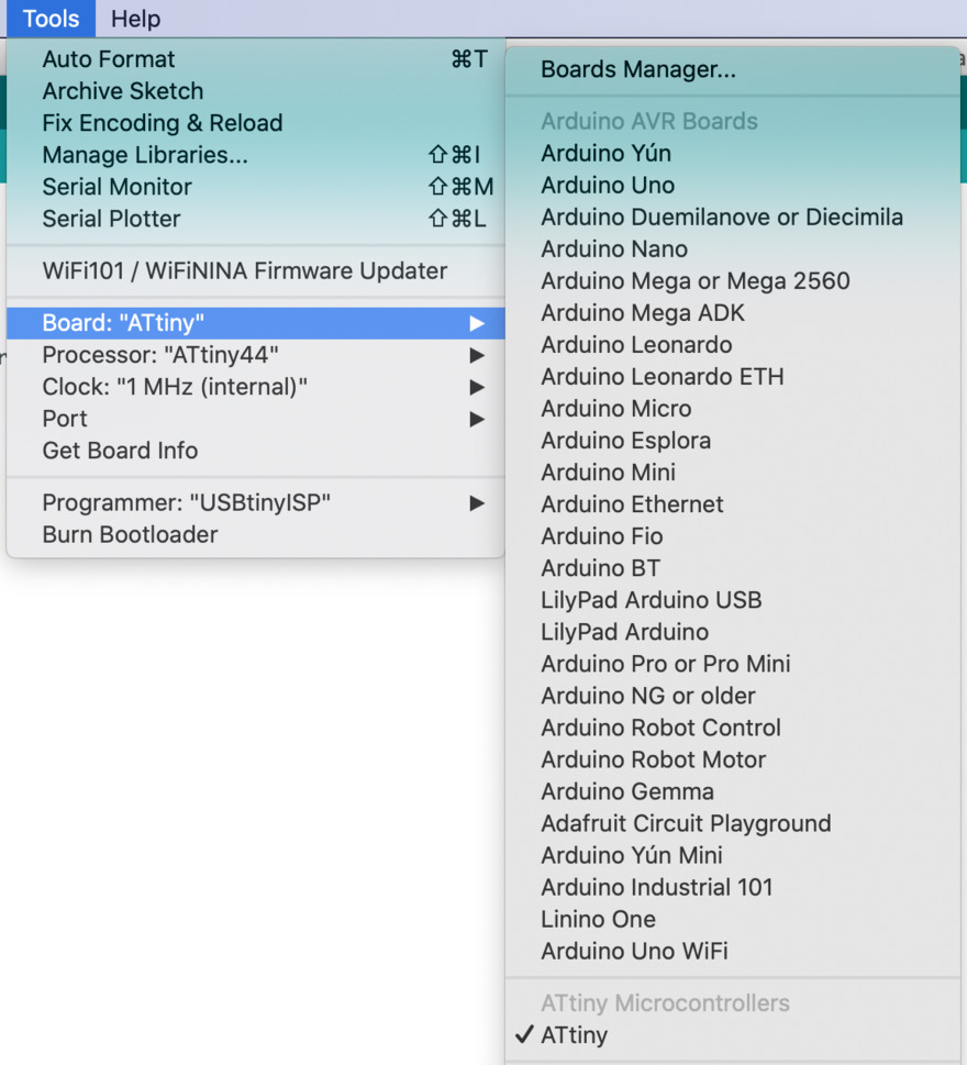
From there, you can go to Tools > Board > Boards Manager. this will bring up a search box. Search ATTiny and install the manager:
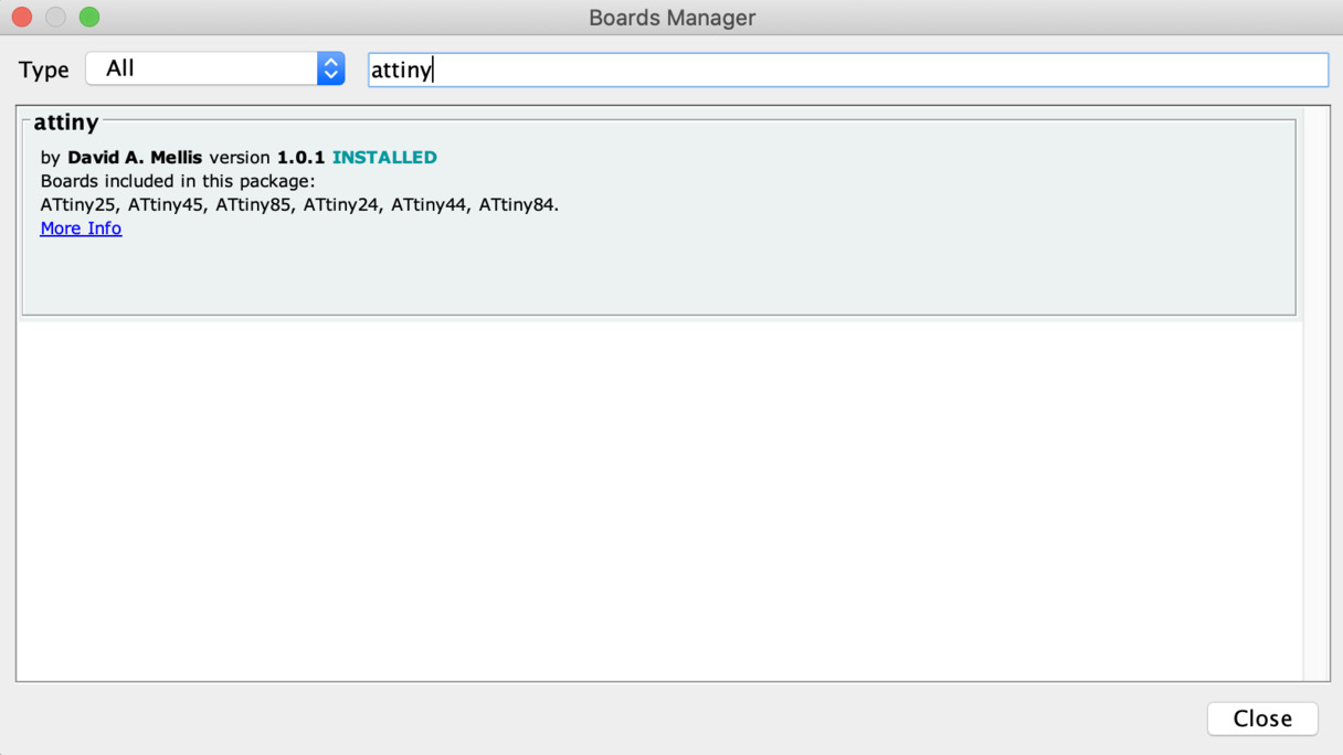
Then, ATTiny will appear as a choice in the Tools > Board menu.
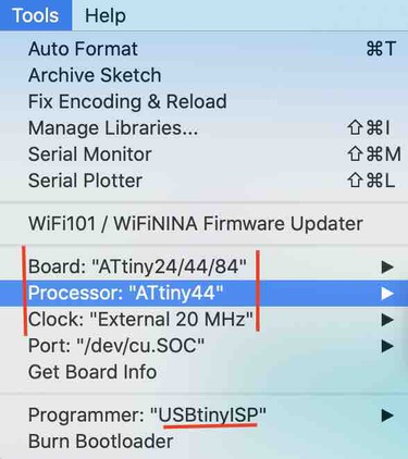
After that, I was able to choose the Tiny44 in the Arduino Tools menu.
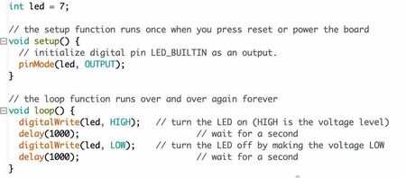
In Arduino I went to File > Examples > Basics > Blink
Once Blink was loaded, I edited the file to match my schematic, which had the LED on pin 7.
The sketch loaded, but sadly the LED did not work. I desoldered it and reversed it, but it still would not go on. I even tried to add an LED for breadboards. So I decided to just try and work with the button.
I tried to run the Arduino example for interacting with a button, modified to work with softwareserial for the attiny, instead of controlling an LED… This also failed, though I think it was a hardware issue. Here is the code I used, having rotated through many different pins attempting to get something to work:
include <SoftwareSerial.h>

#define RX    10
#define TX    11
SoftwareSerial Serial(RX, TX);


// constants won't change. They're used here to set pin numbers:
const int buttonPin = 5;     // the number of the pushbutton pin


// variables will change:
int buttonState = 0;         // variable for reading the pushbutton status

void setup() {
  // initialize the LED pin as an output:
  pinMode(buttonPin, INPUT);
  Serial.begin(9600);
}

void loop() {
  // read the state of the pushbutton value:
  buttonState = digitalRead(buttonPin);

  // check if the pushbutton is pressed. If it is, the buttonState is HIGH:
  if (buttonState == HIGH) {
    // turn LED on:
    Serial.println("on!")
  } else {
    // turn LED off:
   Serial.println("off!")
  }
}
My global reviewer pointed out that, considering the attiny pinout here:
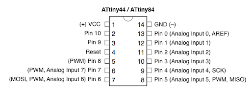 It would have been best to use the configuration
RX, TX = 1 and 0
Button pin =8
LEDpin=7.
I did attempt this configuration, but kept rotating the pin numbers when it failed in hopes that I was only misreading the diagram and confusing pin number for the alternative number listed on the pinmap. This is why the numbers in the sketch above appear somewhat random.
It would have been best to use the configuration
RX, TX = 1 and 0
Button pin =8
LEDpin=7.
I did attempt this configuration, but kept rotating the pin numbers when it failed in hopes that I was only misreading the diagram and confusing pin number for the alternative number listed on the pinmap. This is why the numbers in the sketch above appear somewhat random.
When I could not interact with the button, I decided to give up on this board. At least I could program it! Hero shot of my Frankenstein, barely-functioning board:
For WORKING board design and production, please see my Input Devices or Final Project weeks.
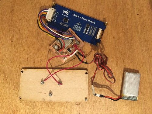
For my final project board, I did not have a button and LED, but did have a touch sensor input and E-Ink output which worked together on the board. Here are images of the board design, the board connected to both input and output, and a final video of the board working as expected. Further description of the process can be found on the project page.