7.Electronic Design
During this week we were introduced to Electronic design where we have to modify echo hello circuit board.
Group assignment
For the group assignment please visit our group page
Design the circuit board
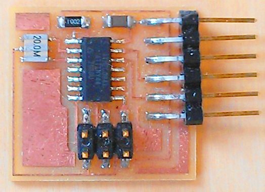
To do so, I used Eagle software to design the circuit board and I have made some modification this was done by adding LED and a Push button
To calculate the resistor value for the LED used, using A simple equation (source volatge - forward voltage)/(forward current) we can calculate the value of the resistor. 5-2.5/0.02 = 125 the closest resistor in our lab was 499.
I placed the components just as Our instructor Hashim taught us with the connector having its VCC side on the right and the GND on the Left and used tags to connect the components together instead of using direct links, hence it would be easier to modify later, and much more comfortable on the eye.
Adding the Electronic components
Fab Library
Firstly, I downloaded the Fab library of Eagle to be able to add all the footprints of the components I need to use. then I faced some difficulties on how to include the library in the software, with a little bit of googling I found this helpful Tutorial by Krishna Verma where it tells you the procedure of how to add a new library.
Adding components
Once the library is added, I started building the circuit by adding all the required electronic component, this done by going to the tool bar then add component >> fab >> select the component you need, I repeated the same thing for all required component, then connecting the components by using net tool. Also, I used the label tool to make the schematic easy to follow.

Board Design
To start with board design go to the tab Generate/switch to board. Then I changed the DRC settings so that the clearance setting is as shown in the picture below,

also, I changed the Minimum Width from the Sizes tab to be 16mil
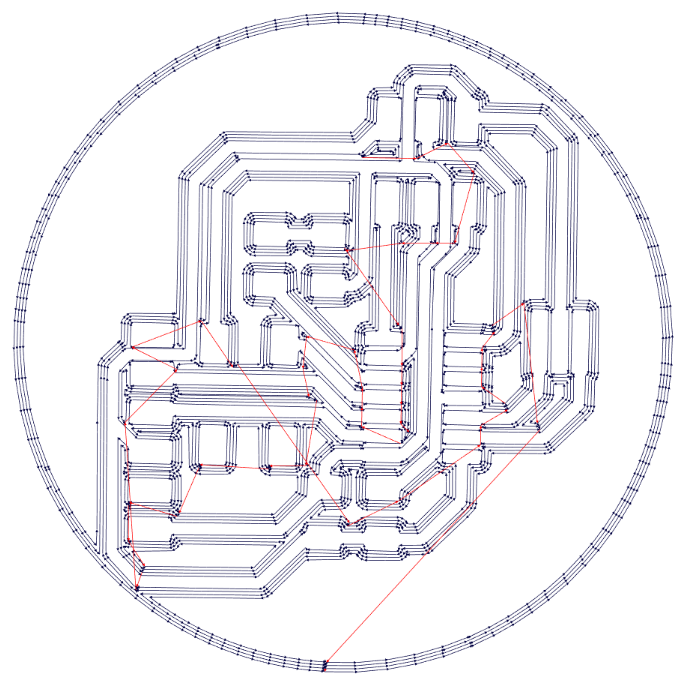
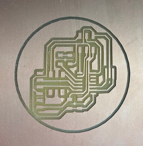
then started placing the footprints of the components following the standard positioning of the ISP, which is placing the ISP just below the ATTINY 44, spending couple of minutes trying to find the best position of the components and with some patience, I reached to following result.

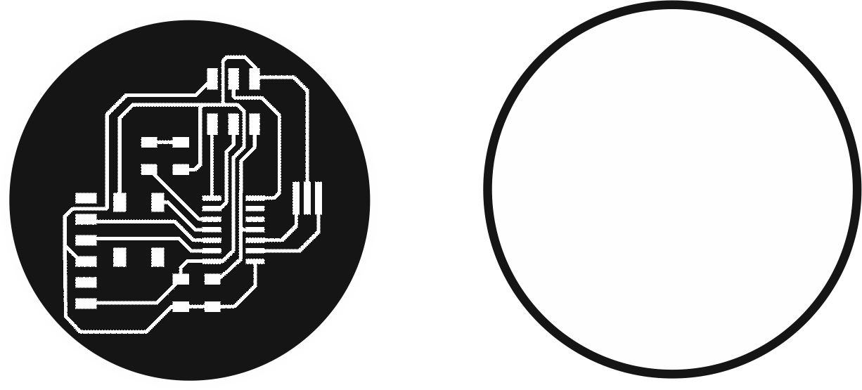
Once I was satisfied with board design I exported the traces to PNG image this done by the following:
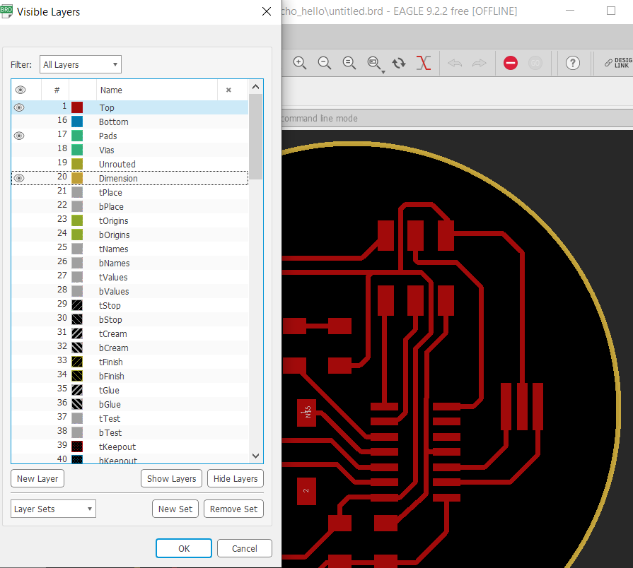
1- Edit Layer settings: hide all the layers except Top, Pads and Dimensions as shown below:
2- Export the PNG image from file>export> image, with resolution of 1000 dpi Monochrome and full area.
Once the Image of the board is generated, I used the coreldraw software to prepare the outline cut and the traces for Fabmodules.org,
then I created the rml file ussing the fab modules and the same steps were followed as the electronics production page,
Then milling the board with the srm 20, and I soldered the components. The exact steps to do so are in the electronics production page.
Board Fabrication
Failure
I followed the same steps as electronic production week, using the monofab SRM-20 to mill my board,
for the first try, the milling was not as expected as you can see from the picture below that there is shortcut in the traces where they touch each other
After investigation I found that when I exported the files in low resolution in coreldraw which was 300 dpi and it should 1000 instead, then I repeated the process again where this time I double checked the resolution making sure it is 1000 dpi,

After milling the board I listed the components as per the schematic and started solder the electronic components paying attention to the polarity and orientation of each one of them.
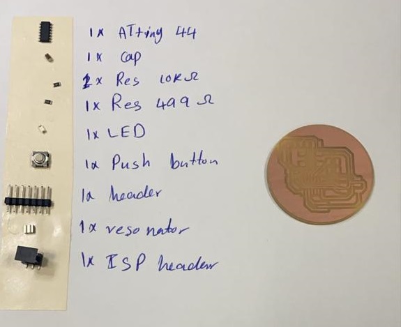
then soldering all the components

and this a video during the embedded programming week showing the board is working where I uploaded a simple code when the push button is pressed the led will blink.
Download Files