7. Electronics design
Assignments for week 6 :
-
This week we have a group assignment and individual assignment .
-
The group assignment for this week is to use the test equipment in my lab to observe the operation of a microcontroller circuit board .
-
The individual assignment for this week is to redraw an echo hello-world board, add (at least) a button and LED (with current-limiting resistor) check the design rules, make it, and test it extra credit: simulate its operation.
The goal for this week was to use the techniques we have learned in the previous weeks as soldering, using the mono fab “PCB cutting”, also to design electronics using different softwares, cut the PCB board and solder the components in order to make it and test it with a button and LED and to use “DRC”, “ERC” which means design rules check and electronics check rules, in order to do that we were given Neil’s Hello world board6 and all the required libraries .
Files to download :
I have included all the files that you need to download down below and here you can find them directly :
Group assignment :
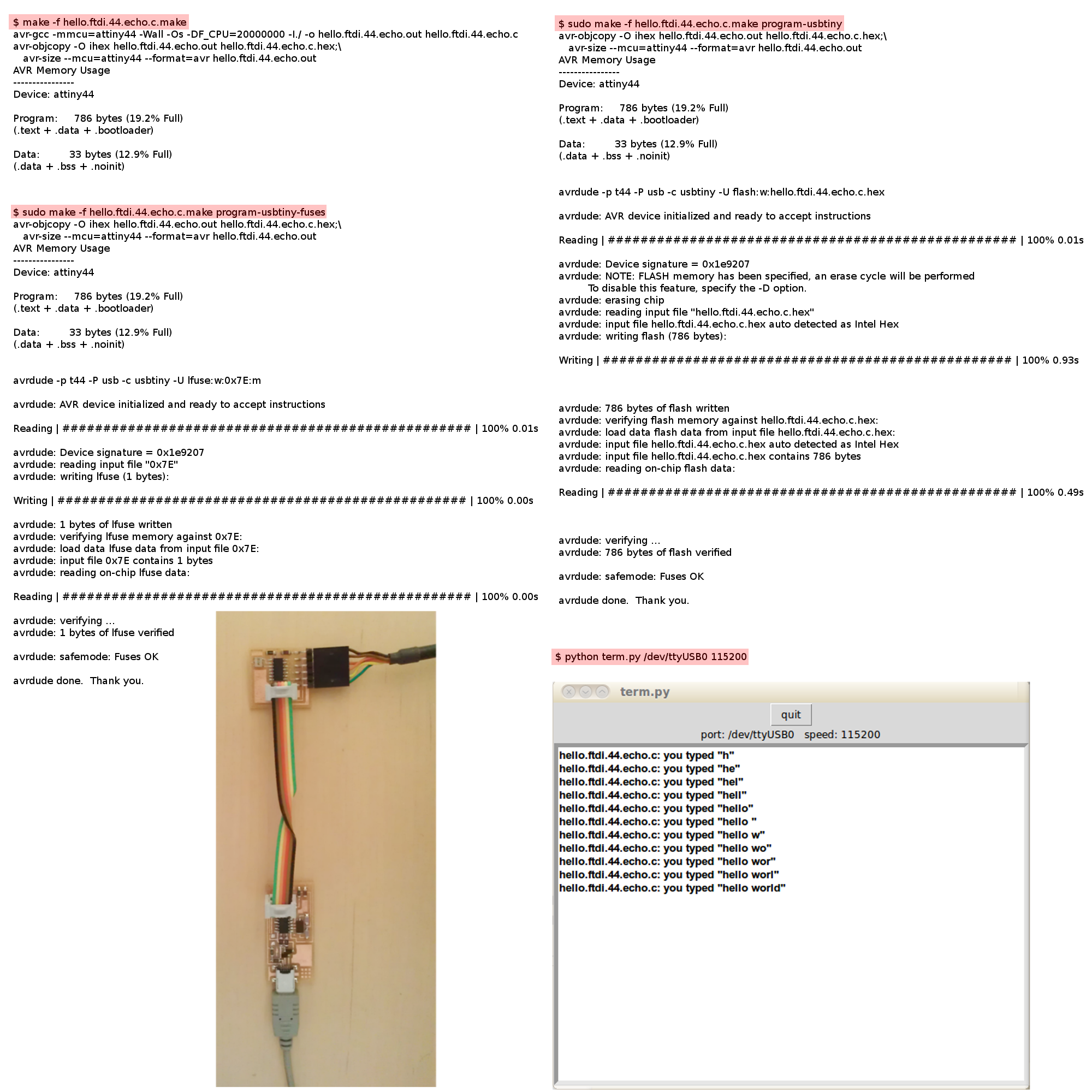
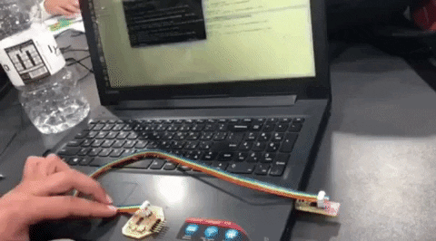
For the group assignment we have to use the test equipment in my lab to observe the operation of a microcontroller circuit board so we used my board and in order to do that we used the digital multimeter to check the continuity between ground pins and VCC pins. Also, we measured the VCC to GND voltage, which should be 5V.
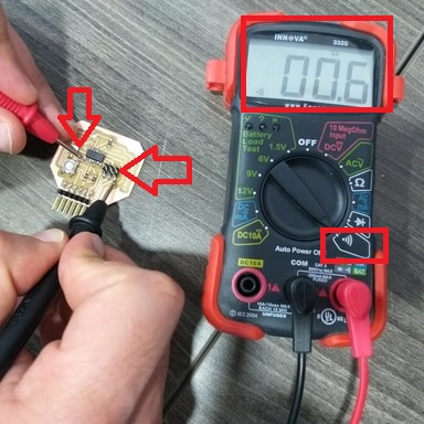
- First we started measuring the continuity between the GND pins of the ATtiny44, ISP header and FTDI header. The digital multimeter should beep and read almost around 0 Ohm and this means all of the three pins are connected and here is a look :
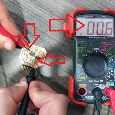
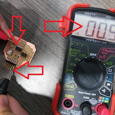
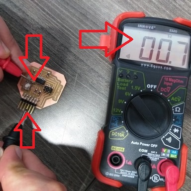
- Second we measured the continuity between the VCC pins of the ATtiny44, ISP header and FTDI header. The digital multimeter should beep and read around 0 Ohm. This means all the three pins are connected and here is a look :
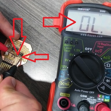
- Third we measured the continuity between the VCC pin and GND pin. The digital multimeter should not beep and read OL (Overload). This means there is no connection (short circuit) between the VCC and GND and here is a look :
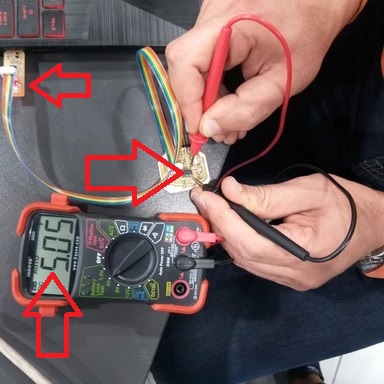
- Last we connected the board to the FabTiny programmer and then to USB. We measured the voltage between the VCC pin and GND pin. The digital multimeter read 5V, which is the USB port voltage.
And thats it all for the Group assignment .
individual assignment :
For the individual assignment i have to to redraw an echo hello-world board, add (at least) a button and LED (with current-limiting resistor) check the design rules, make it, and test it
- In order to design a board you have to use a suitable PCB design software such as : “Kicad”, “EAGLE”, “EasyEDA” and much more of PCB designing softwares and here is my experience with PCB design softwares :
My experience with PCB design softwares :
To sum everything up working with “EAGLE” was really faster and easier because there is no need to download the footprints, also “EAGLE” has a feature called “Auto routing” which helps you more to route and saves time.
Kicad is a good software but needs lots of process such as downloading the footprints, checking every components footprint one by one and much more as you can see in my documentation .
EasyEDA is not bad for beginners and it has lots of good features such as showing your board as a photo or showing the board in 3D mode but for me not as good as “EAGLE or “kicad” .
The components needed :
| Description : | Reference : | Search : | library Name : | Quantity : |
|---|---|---|---|---|
| ATtiny44 | IC1 | tiny | UC_ATTINY44-SSU | 1 |
| Crystal 20MHz | XTAL1 | resonator | XTAL_RESONATOR | 1 |
| Header 3x2 ISP | J1 | ISP | CONN_03X2_AVRISPSMD | 1 |
| Header 1x6 FTDI | J2 | FTDI | CONN_06_FTDI-SMD-HEADER | 1 |
| Capacitor unpolarized 1uF | C1 | cap | CAP_UNPOLARIZEDFAB | 1 |
| Resistor 10kOhm | R1 | resistor | R1206FAB | 1 |
| Resistor 10kOhm | R2 | resistor | R1206FAB | 1 |
| Resistor 499Ohm | R3 | resistor | R1206FAB | 1 |
| Red LED | D2 | led | LEDFAB1206 | 1 |
| Push button | S1 | switch | SW_SWITCH_TACTILE_6MM6MM_SWITCH | 1 |
All the libraries you need :
The program needed :
1. EasyEDA
-
First i started with EasyEDA because i never used it before and here is the process i went throw while designing “Hello world” board :
-
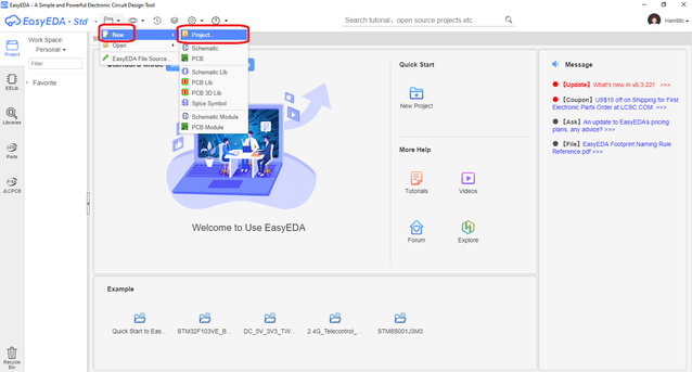
You have to download the software and here is a link Click here and when you open the software you will see this window, you have to register if you dont have an account and open a new project like this :
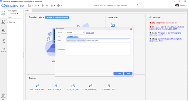
- Now you must give your new project a title also you can put a brief description about your project like this :
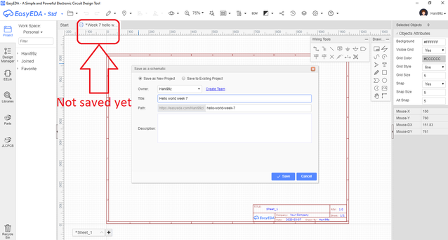
- Then you open a new schematic in order to start adding the components but before that you have to save the new schematic also as the previous step with a title and a brief description like this :
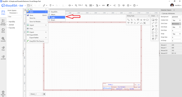
- Before adding any component you have to download the “Fab library” and you can do that by going to >> file >> Open >> EAGLE and that will open the “Fab eagle library” like this :
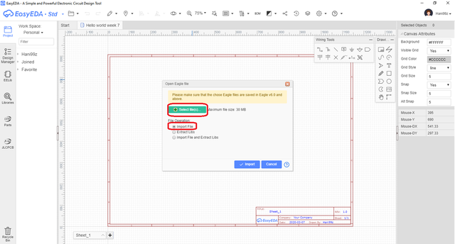
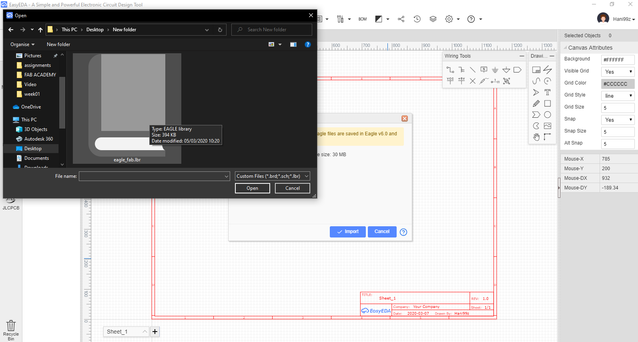
- When doing the previous step this window will show up so you have to select the file and then click on import file then import and now you have the library ready :
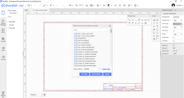
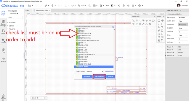
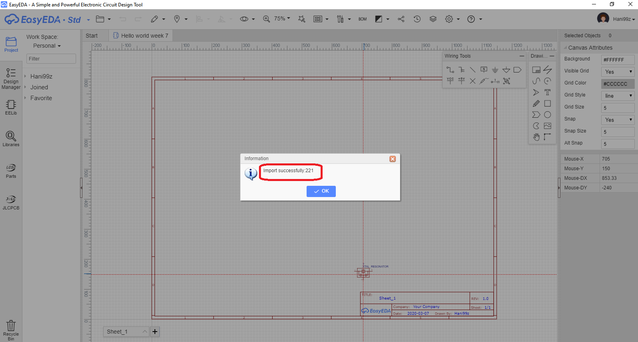
- Now you have to added the components from the library one by one and that is a disadvantage of this software that if you need all the components as my case you will have to go throw all of them and when you finish click on “Added to library” and this message will appear like this :
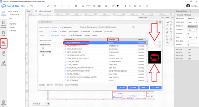
- Now you are ready to added the components you need and in my case i have made a table for the components i need for this week assignment, you can added a component by going to libraries and then search for the component you need and then click on place, i have found this feature in this software very useful that you can search by the component name or by filtering the libraries you have also when you click on the component name and you were not sure if this is the right one the software shows you a picture of how it will look on the board like this :
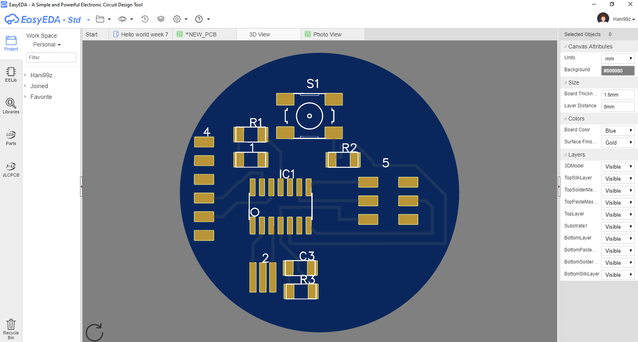
- Here after i have chosen the components i need i started to connect them copying “Neils board”, also i have added “LED” and button, and when i finished the schematics i have converted the schematic into board PCB like this :
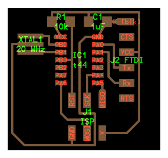
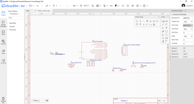
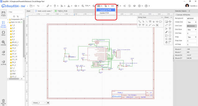
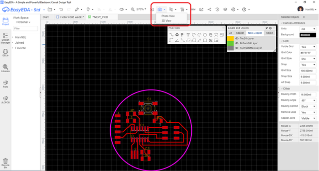
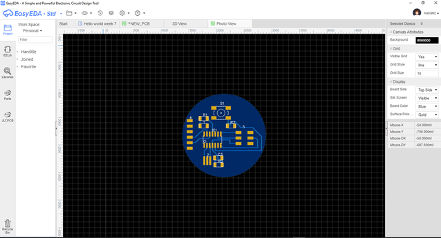
- Now after converting into PCB i have placed the components and connected them, then i have checked if there is anything wrong by checking the schematics again and viewing the PCB as Photo and 3D which considers to be a useful way in this software like this :
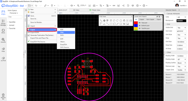
- Here after i have finished wiring and connecting i exported the file as “PNG” by clicking on >>file >> export >> PNG, like this :
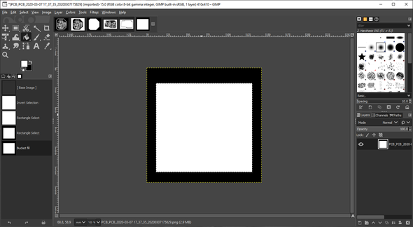
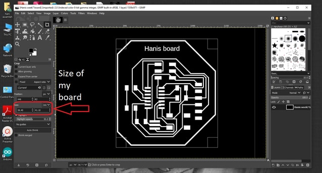
- Here i have opened the file that i have exported and edited it using Gimp in order to make the Outline “interior” and the Traces like this :
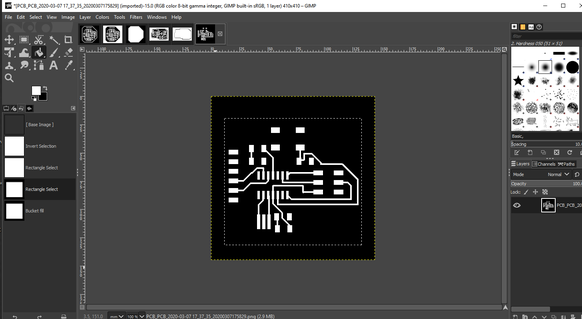
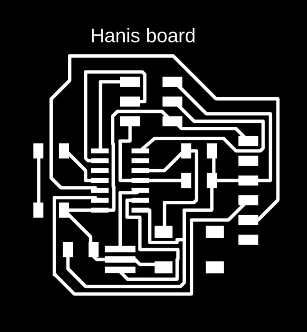
- Here are the traces :
- Here is the interior “outline” :

And thats it for “EasyEDA”
2. Kicad
-
Second i used Kicad because also i never used it so i wanted to learn everything about it and here is the process while designing the “Hello world” board :
-
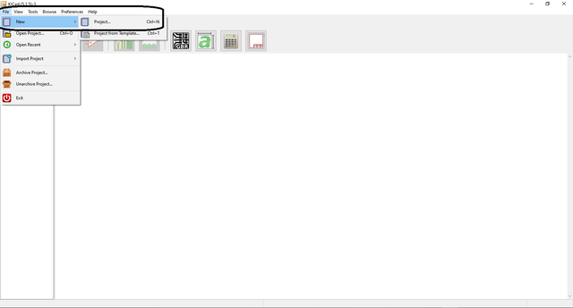
First you have to download the software Click here and when you open the software you will see this window, you have to create a new project from >> file >> new >> project and here is a look :
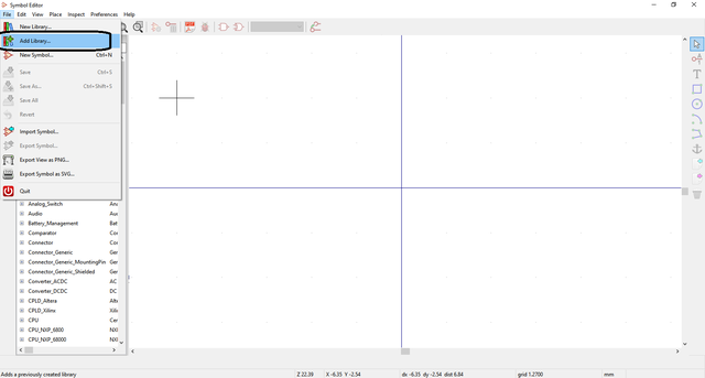
- Now you have to added the library “Fab Kicad library” and its not like “EasyEDA” once you added it you can use directly so no need to added the components, and you in order to added the library by going to >> symbol editor >> add library like this :
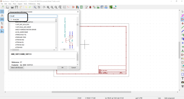
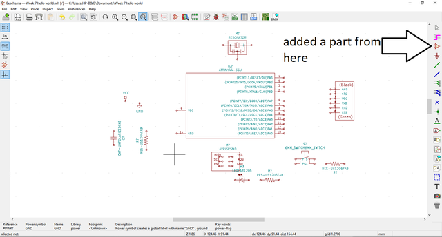
- This is the schematic window where you place the components and connect them, to do that you click on add part on the top right and you look for the library you want to use and its “Kicad fab library” in our case then you search for the components and add them also to make sure you have chosen the right component there is a symbol on the right of the library window like this :
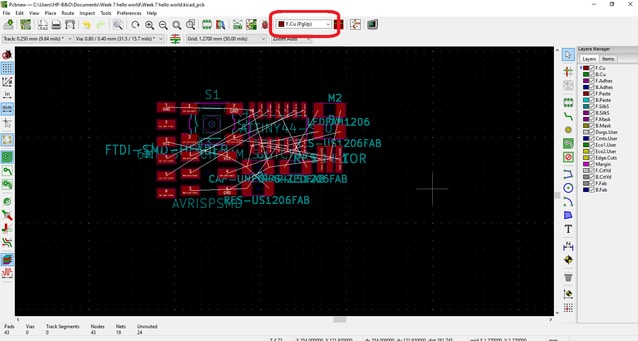
- Here i have added all the components i need in order to make the “Hello World” baord with addition to the LED and the button :
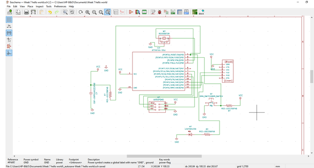
- Here i have connected all the components with respect to “Neil’s board”, also in “Kicad” you have to make sure that all the components have a name also if there are some pins that has no connection you have to place a connection flag on them as you can see :
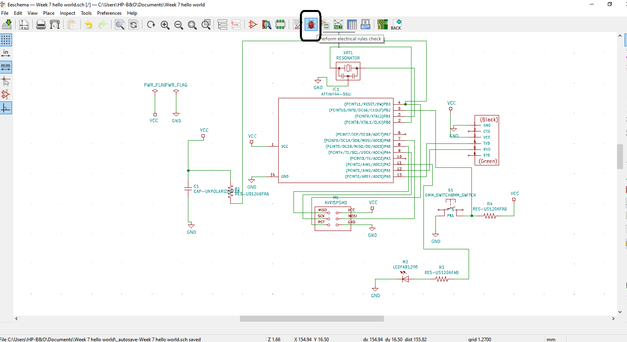
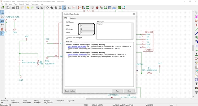
- Now after i connected, named all the components and put a flag on the disconnected pins i have preformed an electrical rules check by clicking on the symbol that is shown in the picture and you can see that there is no Errors :
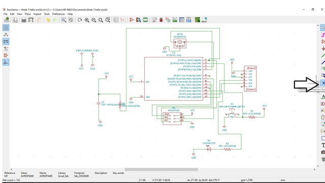
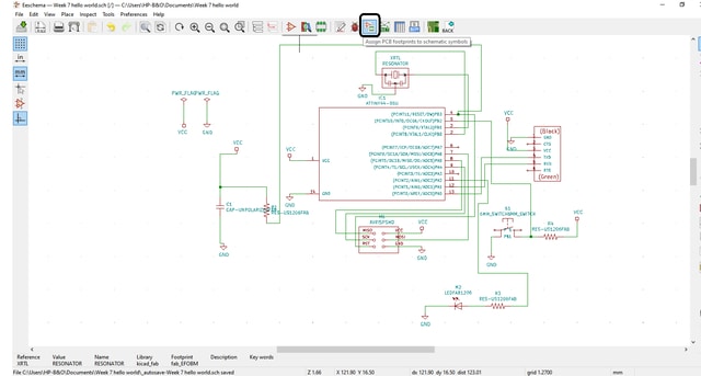
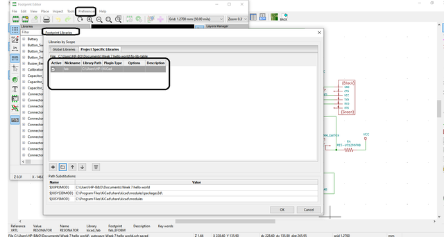
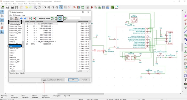
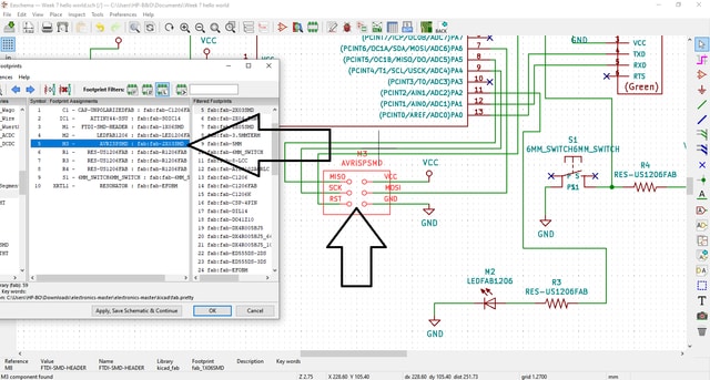
- Now after i have preformed the electrical rules check and made sure there is no errors i have assigned the PCB footprints to the schematic symbols and you can do that by clicking on the symbol shown in the picture and going to >> Footprint editor >> Footprint libraries >> add library, and here is a look :
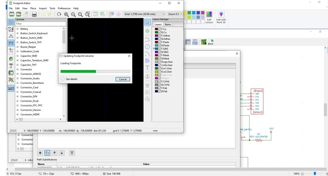
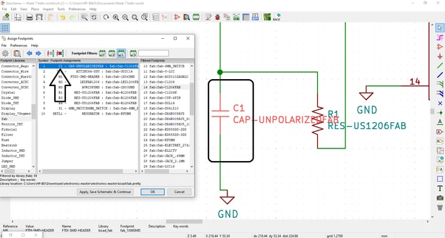
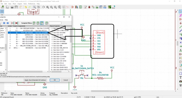
- Now after adding the library the software will update all the libraries in order to show the library we have added as shown, and a confirmation message will appear, click no and the library will be updated, after uploading successfully you have to click on the added library in order to use the new footprints and checking the footprints list one by one and assigning the right footprint as you can see in the pictures :
- Here you can see that the software helps you to check each component you have added and i checked, here is a look for the process :
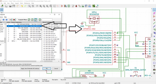
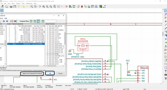
- Finally after checking and making sure i have add all the footprints and all the electrical rules are correct and there is no errors we click on >> Apply save schematic and continue >> ok, as you can see in picture :
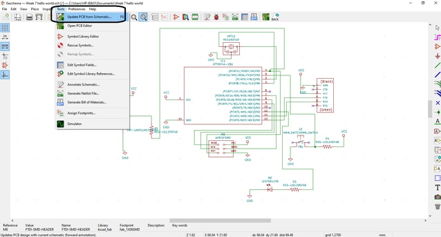
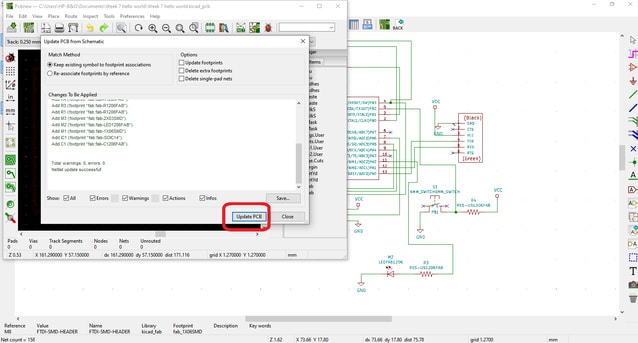
- Now we are ready to update PCB from schematic and you can do that by clicking on >> tools >> update PCB from schematic, and then click on Update PCB after ticking “Keep existing symbol to footprint associations as shown in the pictures :
- Here you can see that we are ready to start designing our board and connecting the components but first you have to make sure you working on the correct layer which is the top “copper” layer as shown :
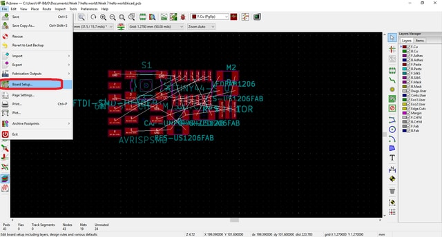
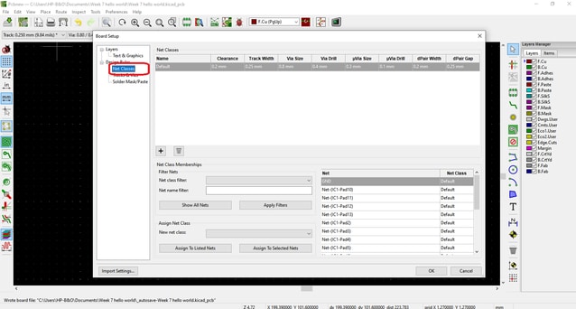
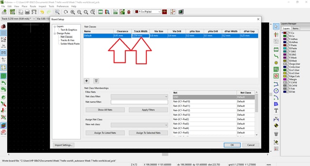
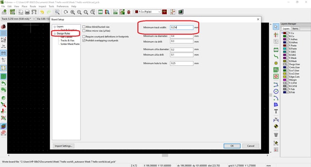
- Before starting to connect the components you have to set up the right settings and to do that you click on >> tools >> board set up, and then a window will appear, from this window click on “Net classes” and from there you have to edit the clearance and the track width also the dpair width must be equal to the track width , then you click on Design rules in order to change the Minimum track width as you can see in pictures :
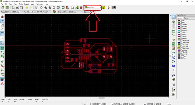
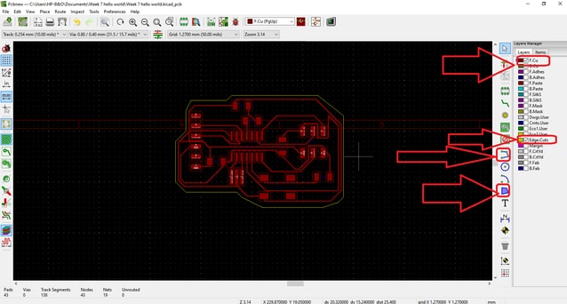
- Here after finishing the connections “traces” you change the layer to “edge layer” in order to make the outline “interior”, after drawing the edge line you have to hide all the layers except for the “edge layer” and the top layer “copper” like this :
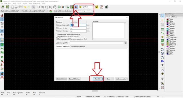
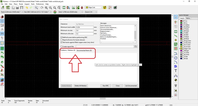
- After finishing all the connections you have to make a “Design rule check” by clicking on the symbol shown in the picture and then running the check by clicking on the button “RUN DRC”, after running the check the software will tell you if you have any Errors and for there were no errors as shown in the pictures :
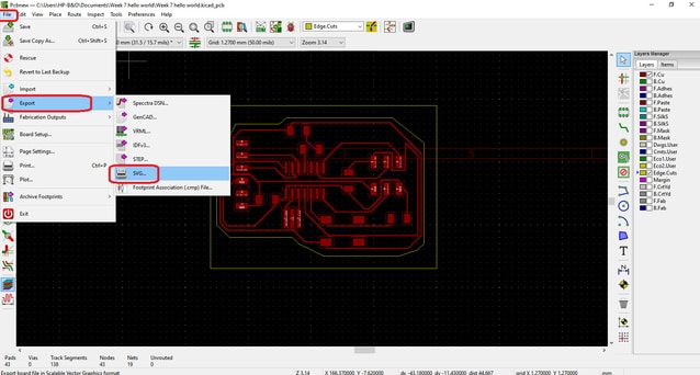
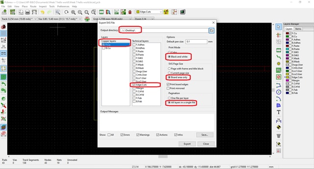
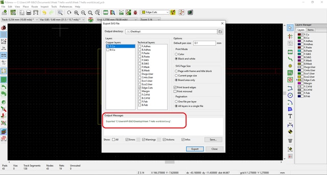
- Now we are ready to export the design as a “SVG” and you can do that by clicking on >> file >> export >> SVG, then a window will appear, in this window you have to put a direction for the design to be saved on, you have to put the layers that you have used and in our case its the top copper layer “F.CU”, the print mode on “Black and white”, SVG Page size to “Board area only” and the Pagination to “All layers to a single file” and then you click on export and a confirmation message will appear to confirm the exportation, and here is a look to this process :
- Here are the traces :
- Here is the interior “Outline” :

And thats it for “Kicad”
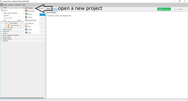
3. EAGLE
-
Third i used EAGLE which i have used before but i wanted to learn more and more about this software and here is the process while designing the “Hello world” board :
-
First you have to download the software Click here and when you open the software you will see this window, you have to create a new project from >> file >> new >> project and here is a look :
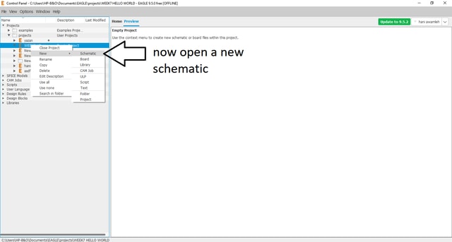
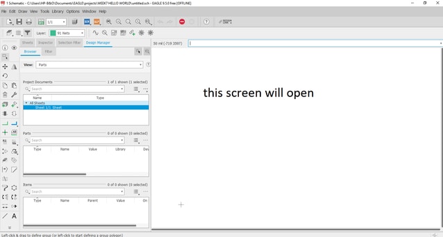
- Now you have to open a new schematic by going to >> file >> new >> schematic, and when you click on schematic this window will open, here is a look :
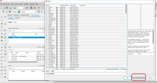
- In this window you can added parts from the symbol “added part” as shown in the picture but first you have to download the library “fab library”, which you can find on top, in order to do that click on add part and then go to “library manager” and then go to “available” and browse for the library you have downloaded and click on “use” and here is a look on how to do it :
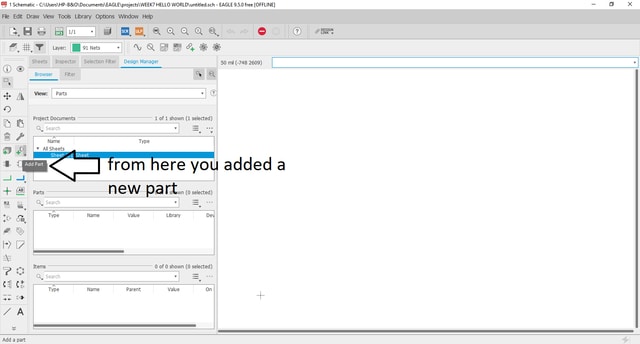

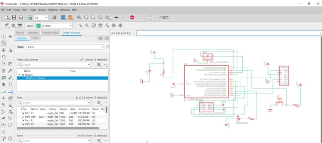
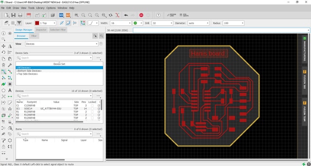
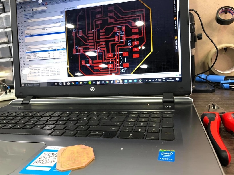
- Now you can added the required parts for the design and in my case i have made a table on top of the parts i need to create the board and here is a look to the schematics :
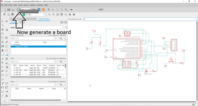
- After finishing the schematic now you can generate a board and to do that click on the symbol shown in the picture like this :
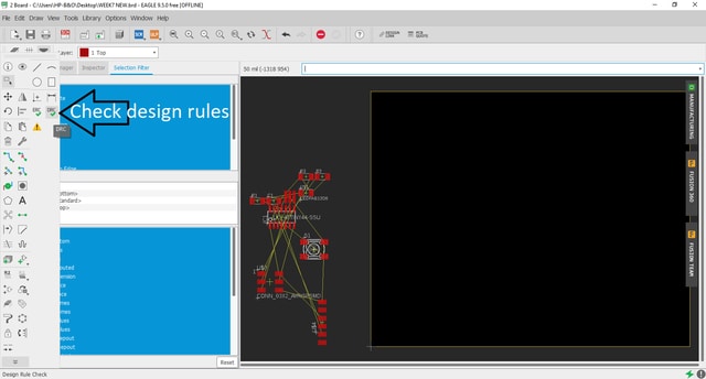
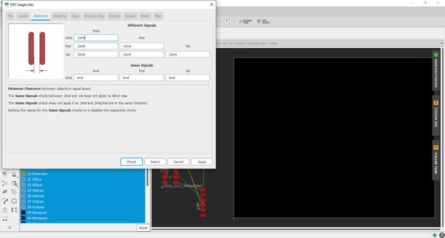
- This window will appear when you click on generate a board but before doing any routing you have to upload the “Design rules check” in order to make sure that all of your connections are right and to do that you click on the symbol” “DRC” and then click on apply, when you finish all your connections you go back to “DRC” And click on check in order to see if there is any errors like this :
-
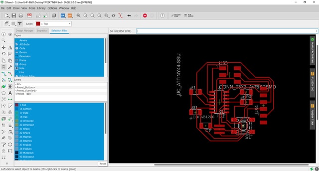
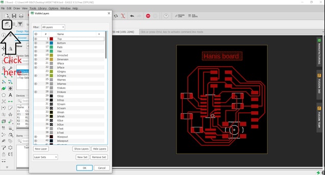
Here i have finished all the connections “only one layer which is top layer” and made the edge cut, also i have hidden all the layers that are not used or needed in order to export the design as an image, to hide the layers you click on the symbol shown in the picture like this :
-
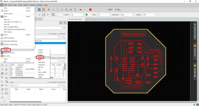
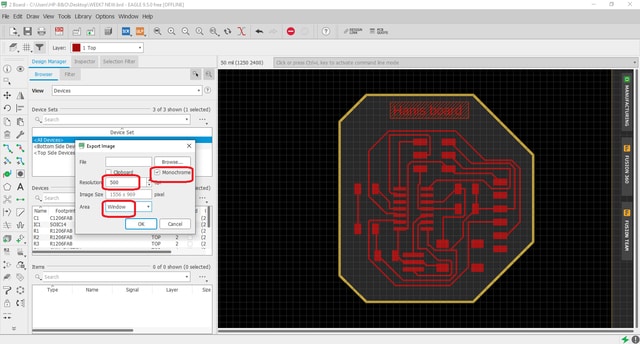
Now we are ready to export the design as an image and to do that go to >> file >> export >> image, and a small window will appear as shown in the picture, in this window you click on “monochrome” and the “resolution” can be “500” or “1000” also click on “Area” and choose window then put a “location” and click OK and the design will be exported as you can see in the pictures :
- Here i have opened the image using Gimp in order to see my design area and to edit it and crop it like this :
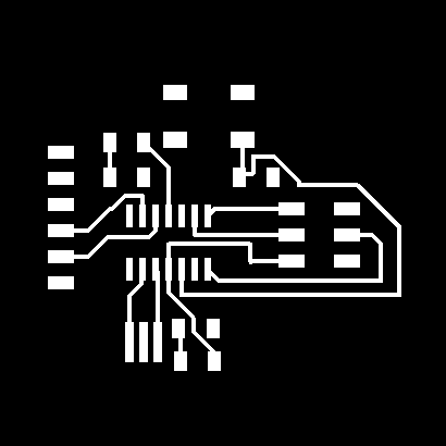
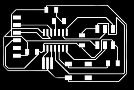
- Here are the traces :
- Here is the interior “Outline” :

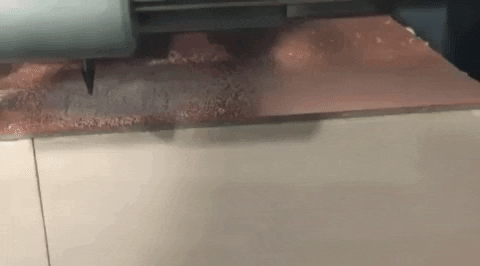
And to complete the assignment i have chosen to cut the board i have designed on eagle
-
Before cutting you have to go back to week 4 in order to know all the safety rules and the right milling bits used in cutting the traces and the interior, also to know how to use mods and how to put the right settings for the machine .
-
Here is the process of cutting the traces :
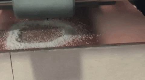
- Cutting the interior :
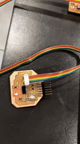
The hero shot of the individual assignment :
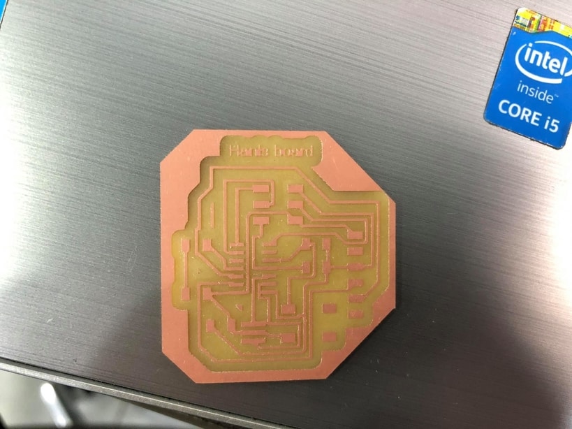
Errors and solutions :
-
Here i have soldered the components and tested the board but unfortunately some errors happened and here is a list of the errors :
-
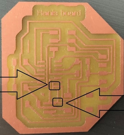
As you can see in this picture there was a short circuit between the Attiny 44 pins which was the reason that the board when programmed no output is given and i did not notice at first which made me think that the schematics were wrong or the connection of the board design were wrong and i have made that clear by checking “Neils hello board” and that was not the problem :
 .
. -
the reason of this short circuit goes back to board design which seems that the traces are really close that the milling bit did not cut .
-
The reason why the milling bit did not cut because in the board design it seems that i have forgot to check the design rules check .
-
Finding this error took me three days and at first i thought the problem is with the solder or that i have placed the components in a wrong way or the problem was from my ISP programmer but tracking these thoughts one by one i have reached to the main problem which was that i have forgot to check the design rules and the board was not programmed .
-
The solutions :
-
In order to make clear that the ISP is connected 100% to my board i have tested it by using the multimeter and it was clear then that the problem was not the connection because it gave me a read of 5 volts, so by that i was sure that the board is connected .
-
Also to make clear that the Attiny 44 is working properly i have connected it to my ISP and i have seen that the computer recognize it so i did programmed it but unfortunately still did not give me the output needed :
-
Finally i have noticed that the short circuit was in board and that happened when i cut the board again and started to check every trace by the multimeter and at last i have found the problem and corrected it .
-
I wanted to design the board again but as an engineer we dont leave the problem we fix the problem and different techniques in order to fix it and for me finding the problem was the best experience i have learned this week so i kept searching for the problem and trying different scenarios and finally i have known the problem and fixed it .
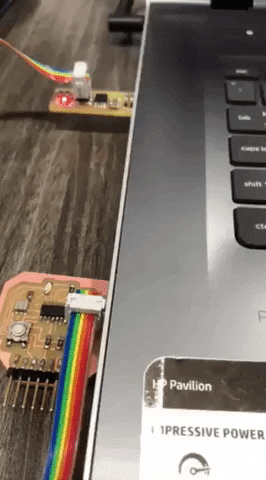
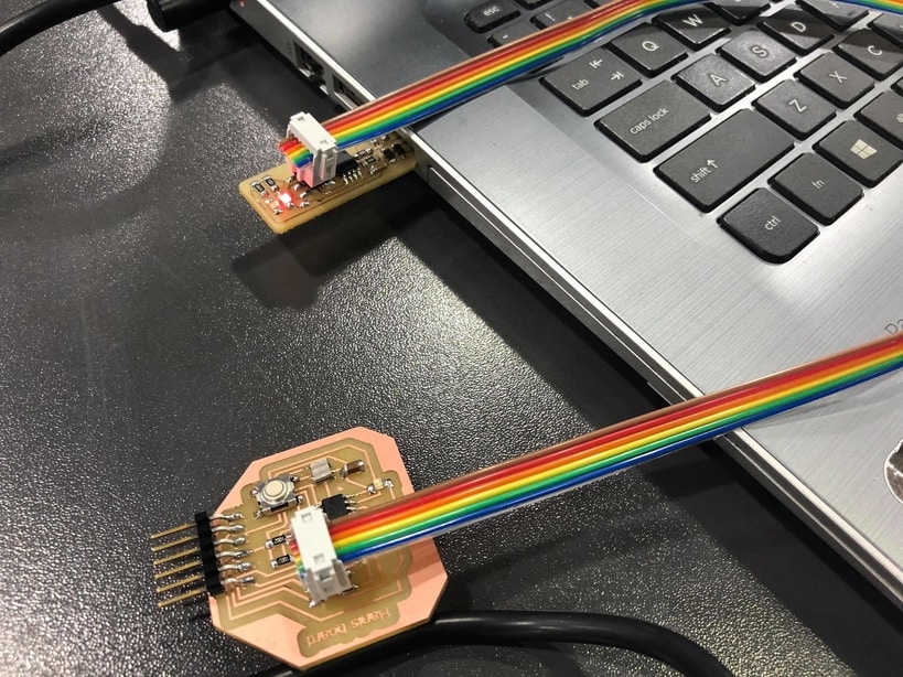
Here is the final result :
- After solving the problem everything works now and here is a look :
Click here to download the board
Click here to download the schematic
- Here is a video of the board working properly :