7. Electronics Design
Group Assignment
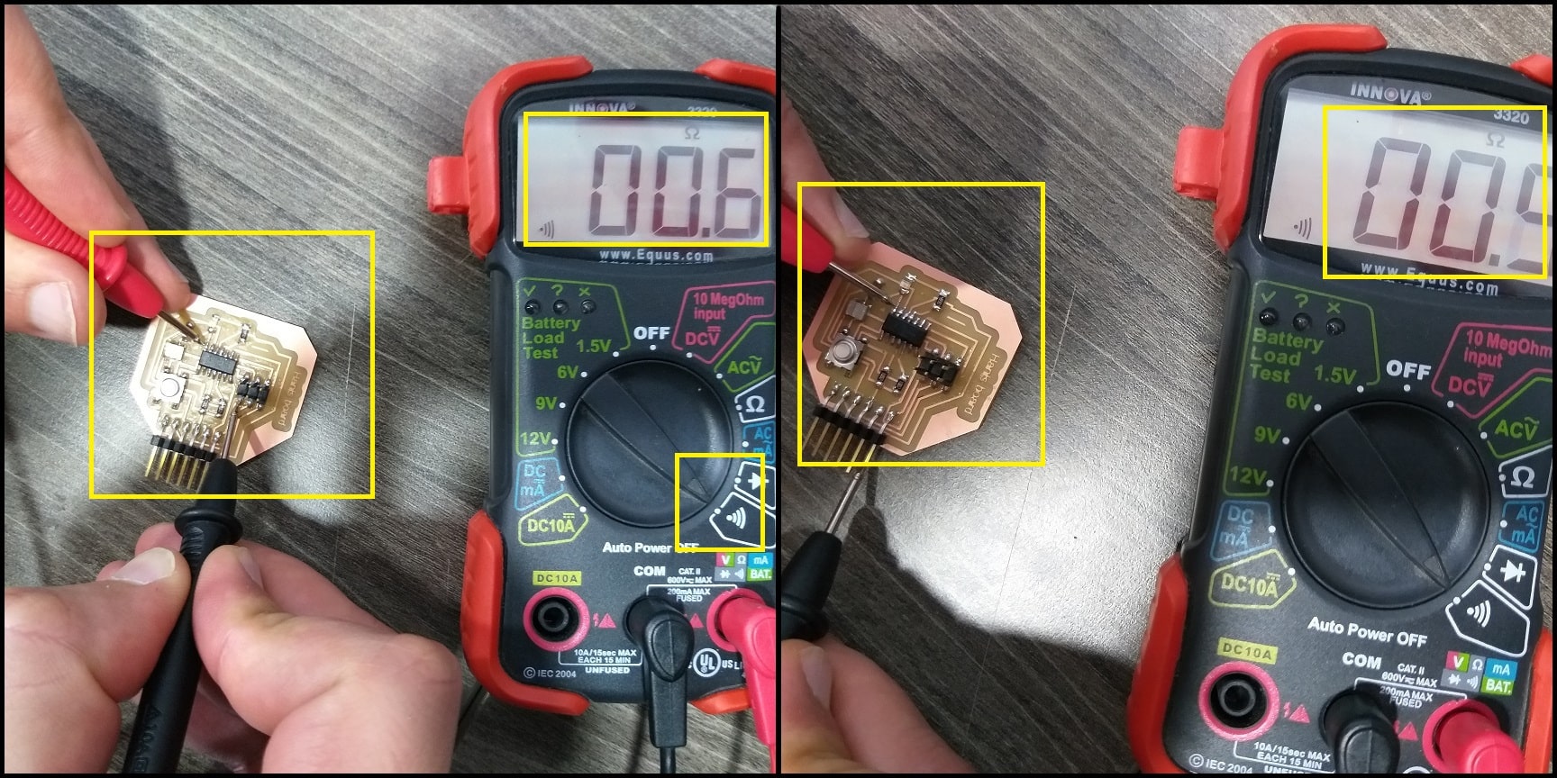
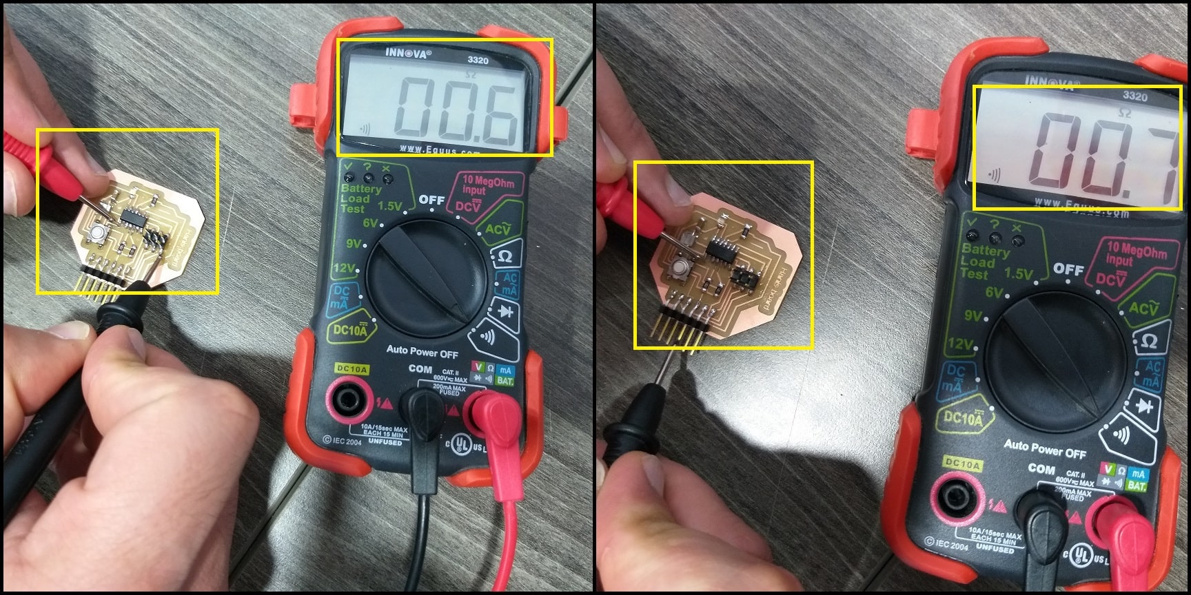
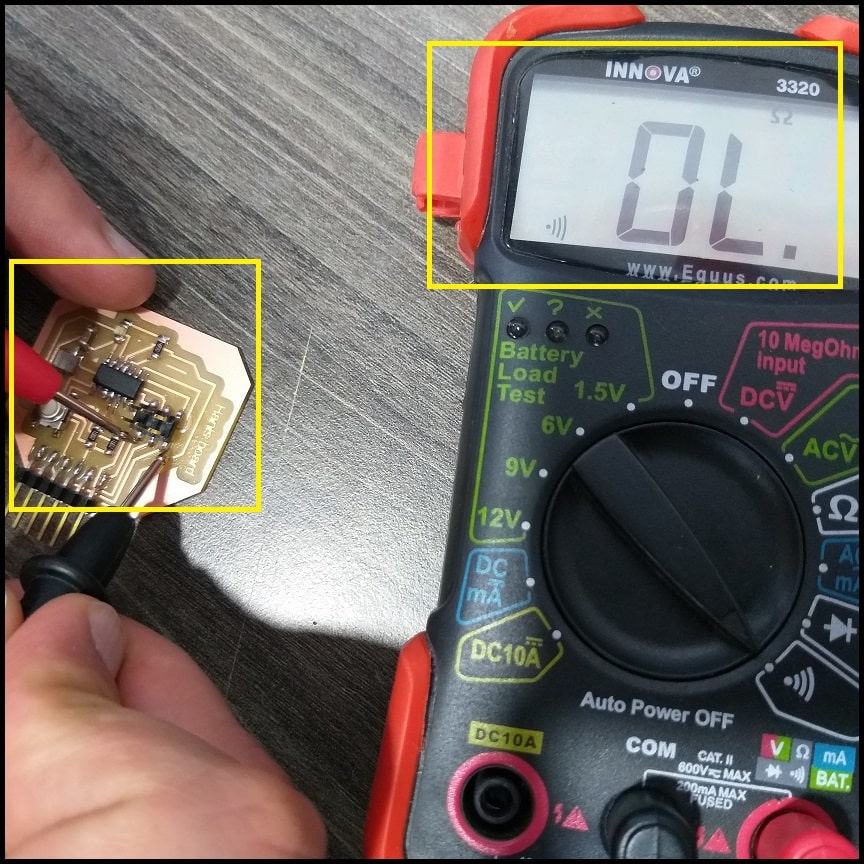
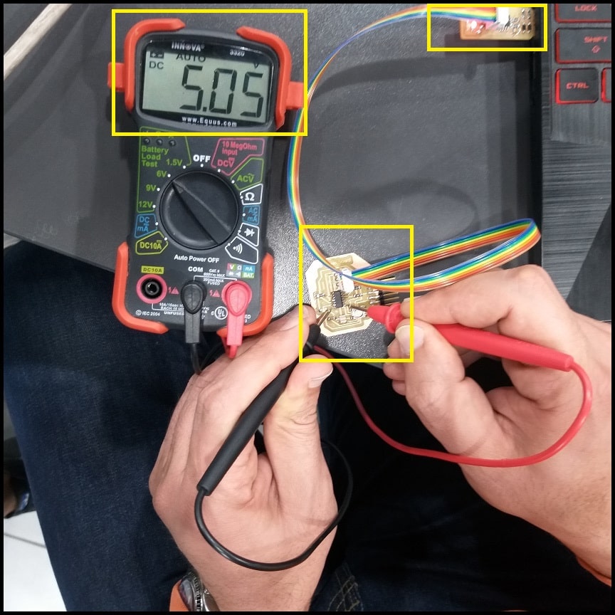
In group assignment we used the digital multimeter to check the continuity between ground pins and VCC pins. Also, we measured the VCC to GND voltage, which should be 5V.
GND (Ground) Continuity
We measured the continuity between the GND pins of the ATtiny44, SPI header and FTDI header. The digital multimeter should beep and read around 0 Ohm. This means all the three pins are connected.
VCC (5V) Continuity
We measured the continuity between the VCC pins of the ATtiny44, SPI header and FTDI header. The digital multimeter should beep and read around 0 Ohm. This means all the three pins are connected.
VCC-GND Continuity
We measured the continuity between the VCC pin and GND pin. The digital multimeter should not beep and read OL (Overload). This means there is no connection (short circuit) between the VCC and GND.
VCC to GND Voltage
We connected the board to the FabTiny programmer and then to USB. We measured the voltage between the VCC pin and GND pin. The digital multimeter read 5V, which is the USB port voltage.
Week Assignment
File Download
ATtiny44 datasheet
Echo hello-world ATtiny44 board original design
Echo Hello-World Board Using Eagle
Software: Eagle
File Download
Eagle Fab library (.lbr) and design rules (.dru)
Eagle echo hello-world ATtiny44 ZIP file
Eagle echo hello-world ATtiny44 board traces png file
Eagle echo hello-world ATtiny44 board interiors png file
Eagle echo hello-world ATtiny44 board traces rml file
Eagle echo hello-world ATtiny44 board interiors rml file
“EAGLE is a scriptable electronic design automation (EDA) application with schematic capture, printed circuit board (PCB) layout, auto-router and computer-aided manufacturing (CAM) features. EAGLE stands for Easily Applicable Graphical Layout Editor.” (Source).
In this part I redrew the echo hello-world ATtiny44 board using Eagle and added two LEDS and a push button.
Redrawing the Echo Hello-World board
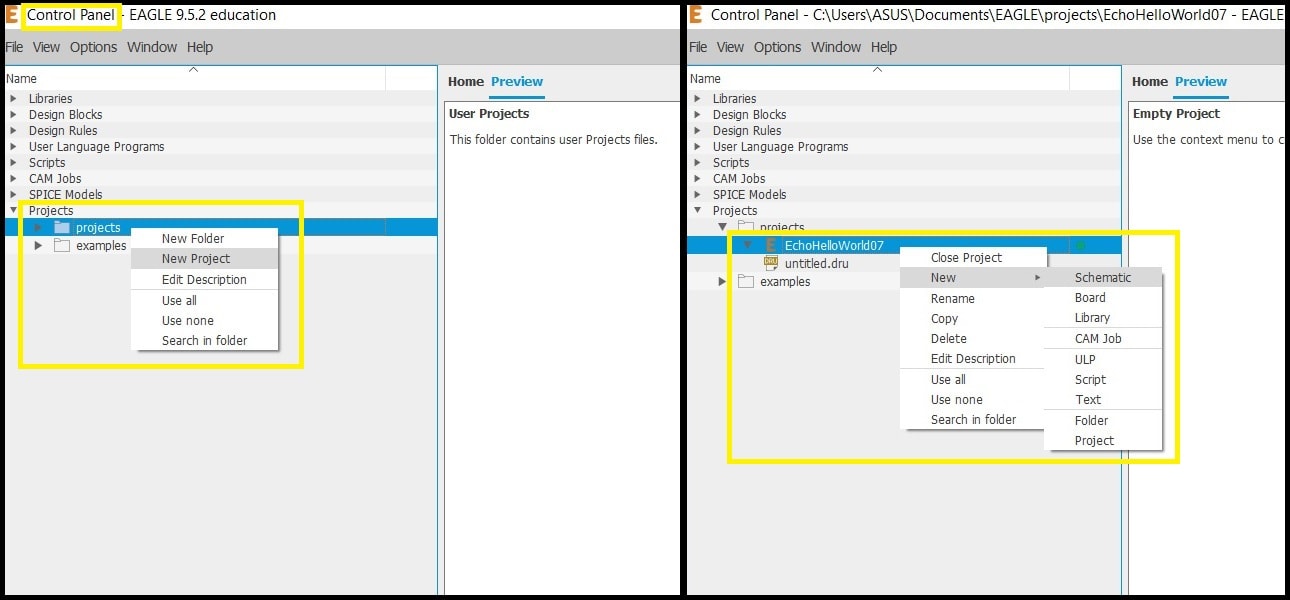
Step 1: Open Eagle software. This is the “Control Panel”. Right click on “Projects” and then select “New Project” and name it. I called mine “EchoHelloWorld07”. This will be the container for the schematic and PCB.
Step 2: Right click on your project and select “New > Schematic”. This will add a schematic to your project and open the “Schematic Editor”.
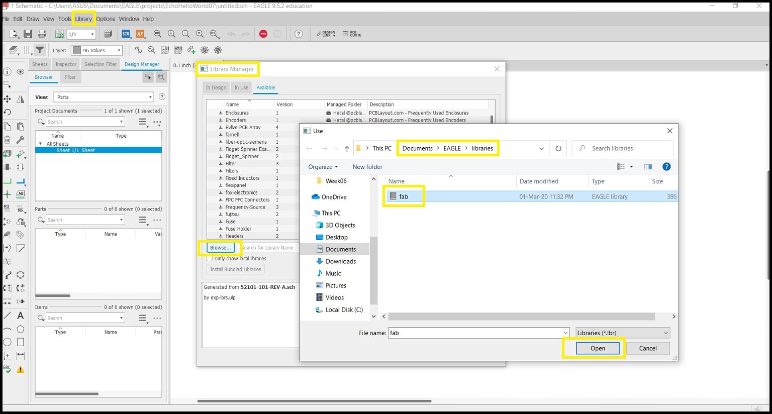
Step 3: First we will add Eagle fab library (fab.lbr). Download the file and unzip it. I unzipped it in “..\Documents\EAGLE\libraries”.
In Schematic Editor go to “Library > Open library manager” and then select “Available” tab. Click on “Browse” and locate fab.lbr on your drive. Click “Open”. This will add fab.lbr to “Available” libraries list.
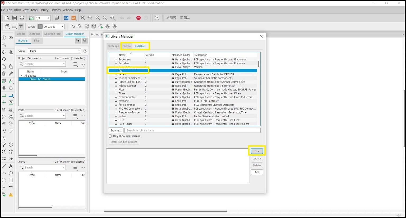
Step 4: Select fab.lbr in list and click “Use”. This will move fab.lbr to “In Use” list and make all components defined inside accessible in schematic editor. close “Library Manager”.
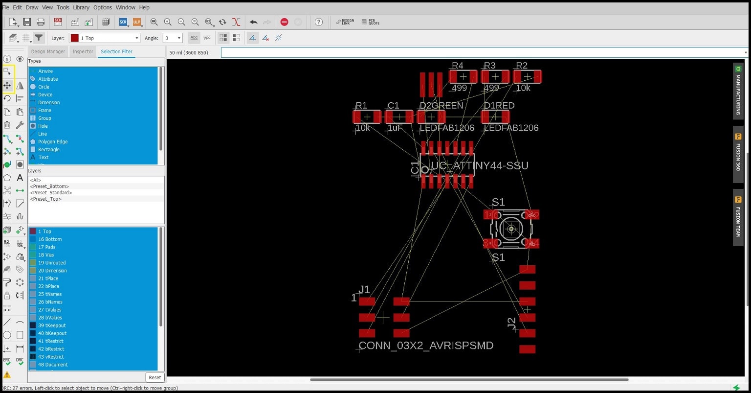
Step 5: First we will add to schematic the components of the original echo hello-world board. Click on “Add Part” and in search field look for “*tiny*“. Double click on “UC_ATTINY44” under fab library. Select “UC_ATTINY44 - SOIC14” and click “OK”. Click on schematic editor work area to place the part. Use “Name” and “Value” tools and click on “+” mark on component to change the name and value.
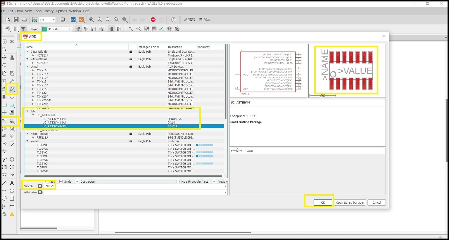
| Description | Reference | Search | Lib Name | Qty |
|---|---|---|---|---|
| ATtiny44 | IC1 | *tiny* | UC_ATTINY44-SSU | 1 |
| Crystal 20MHz | XTAL1 | *resonator* | XTAL_RESONATOR | 1 |
| Header 3x2 ISP | J1 | *ISP* | CONN_03X2_AVRISPSMD | 1 |
| Header 1x6 FTDI | J2 | *FTDI* | CONN_06_FTDI-SMD-HEADER | 1 |
| Capacitor unpolarized 1uF | C1 | *cap* | CAP_UNPOLARIZEDFAB | 1 |
| Resistor 10kOhm | R1 | *resistor* | R1206FAB | 1 |
Repeat for all items in the table and remember to look in fab library.
Step 6: Add components in table below to the original echo hello-world ATtiny44 board. Work through the same steps to add to schematic. Remember to save your schematic. I saved it under “helloWorld44”. Add “VCC” and “GND” to the schematic.
| Description | Reference | Search | Lib Name | Qty |
|---|---|---|---|---|
| Resistor 10kOhm | R2 | *resistor* | R1206FAB | 1 |
| Resistor 499Ohm | R3, R4 | *resistor* | R1206FAB | 2 |
| Green LED | D1 | *led* | LEDFAB1206 | 1 |
| Red LED | D2 | *led* | LEDFAB1206 | 1 |
| Push button | S1 | *switch* | SW_SWITCH_TACTILE_6MM6MM_SWITCH | 1 |
Your schematic should look similar to the image below. You can arrange components in schematic as your preference.
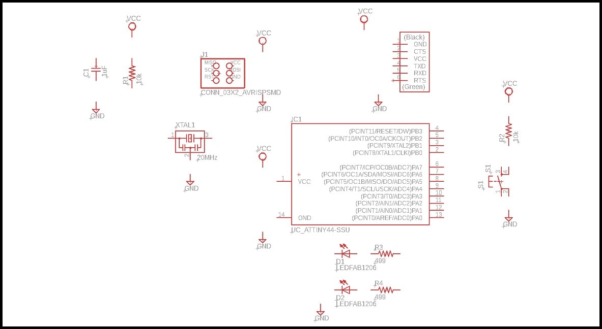
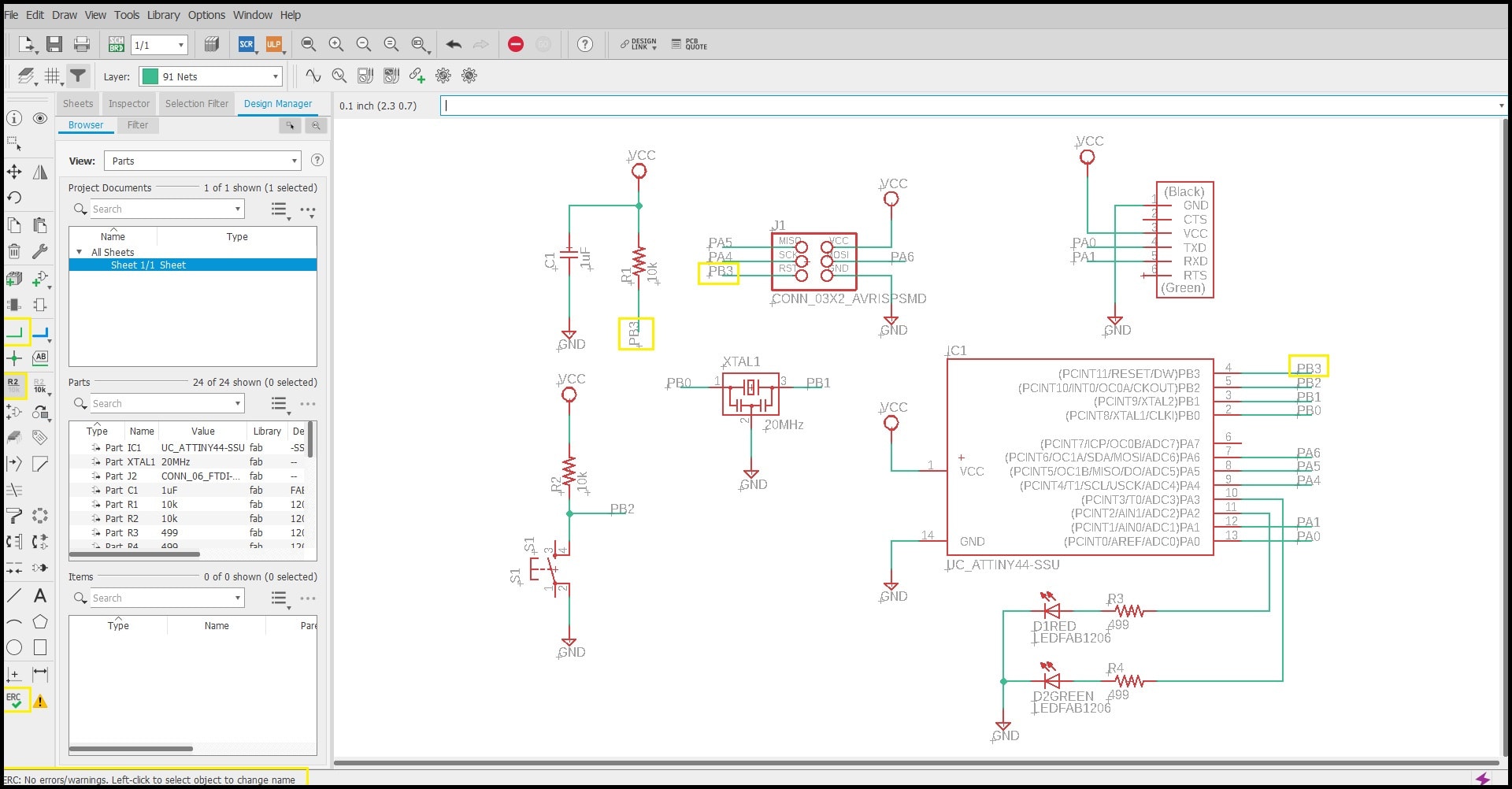
Step 7: As per the original echo hello-world ATtiny44 board and using “Net” tool, add wiring to components. Make direct connections between components when possible. Using “Name” tool add names to open connections. Using names makes schematic less messy and works the same as direct connection between components. For example all open connections named “PB3” are connected together. Click “Yes” when asked to make connections.
Click on Electrical Rule Check “ERC” to see if there are any errors or warnings in your schematic.
Making the PCB
Step 1: Now the schematic is ready to create the PCB. in “Schematic Editor” go to “File > Switch to board”. Click “Yes” for the warning message “Create from schematic?”. “Board Editor” window opens and all components are placed using there footprints and connections made in schematic editor.
Click on “Group” and draw around your components. Select “Move” and right click on components and select “Move: group”. Place your components to the center of board.
Step 2: Fine yellow wirings represent the connections made in the schematic. All those wirings should be replaced using “Route Airwire” tool.
Before we start, we need to load design rule check file (fabcity-designrules.dru). Download the file and unzip it. I unzipped it in “..\Documents\EAGLE\design rules”. In Board Editor go to “Tools > DRC…” and then select “File” tab. Click on “Load” and locate fabcity-designrules.dru on your drive. Click “Open” and then “Apply”. The DRC window title is changes to DRC (fabcity-designrules). Click “Select” to close the DRC window.
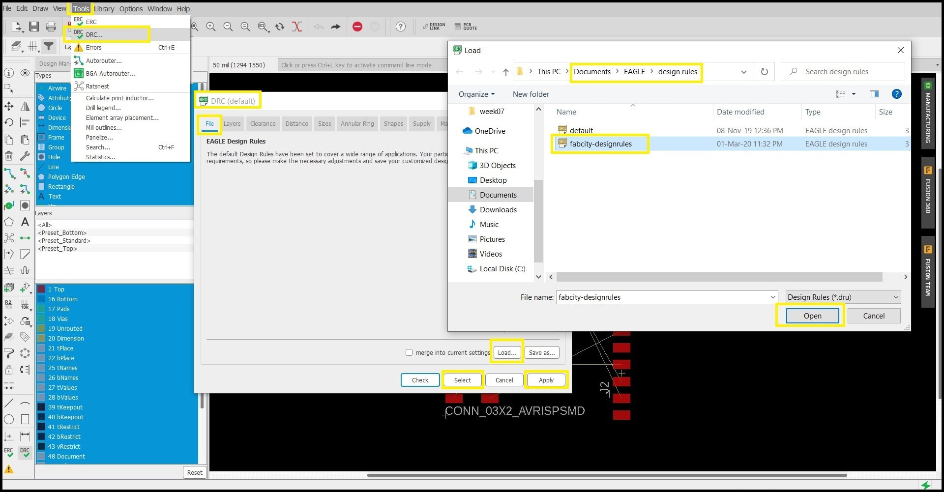
Step 3: Use “Route Airwire” tool to replace fine yellow connections and route between your components. You may take some time to find a good positioning for components. Minimum route width is defined in fabcity-designrules.dru 10 mil (0.254 mm) and also minimum spacing between routes 16 mil (0.41 mm) to fit with 1/64” milling bit. Note that all routes are part of layer “1 Top”.
Click on Design Rule Check “DRC” and then “Check” to see if there are any errors or warnings in your board.
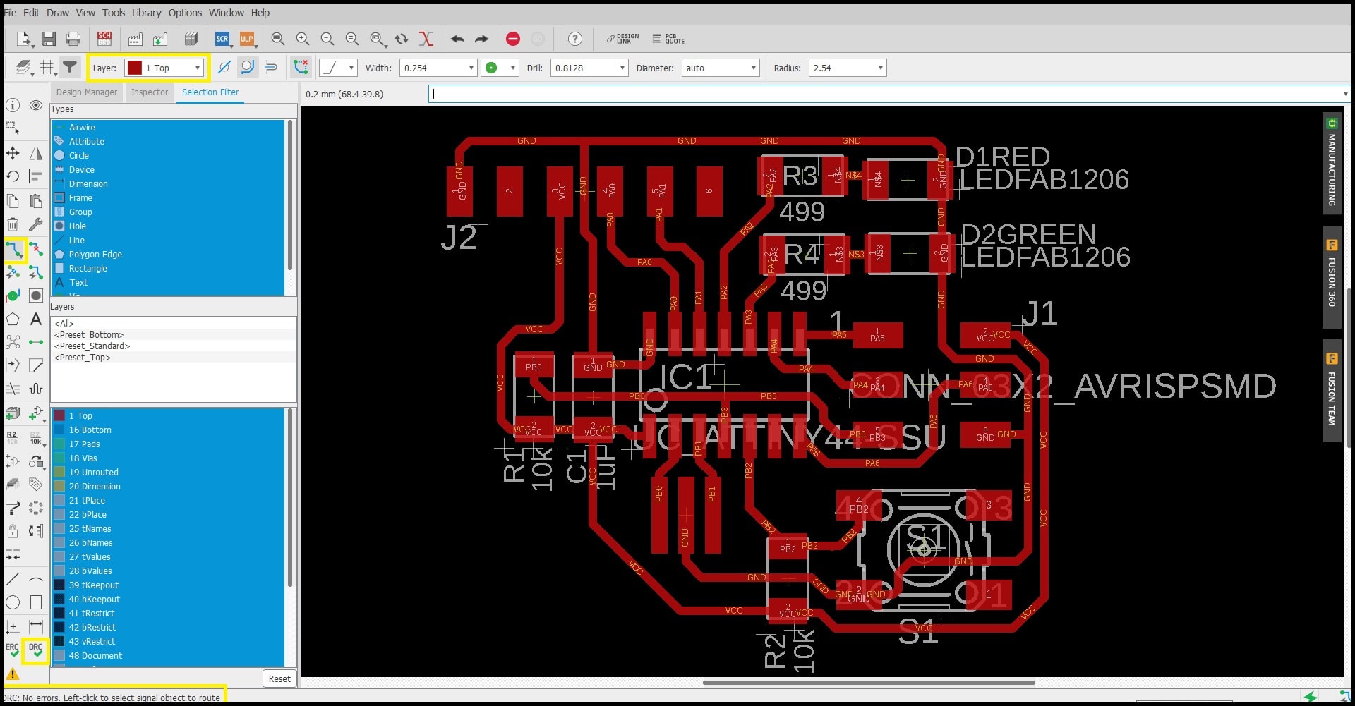
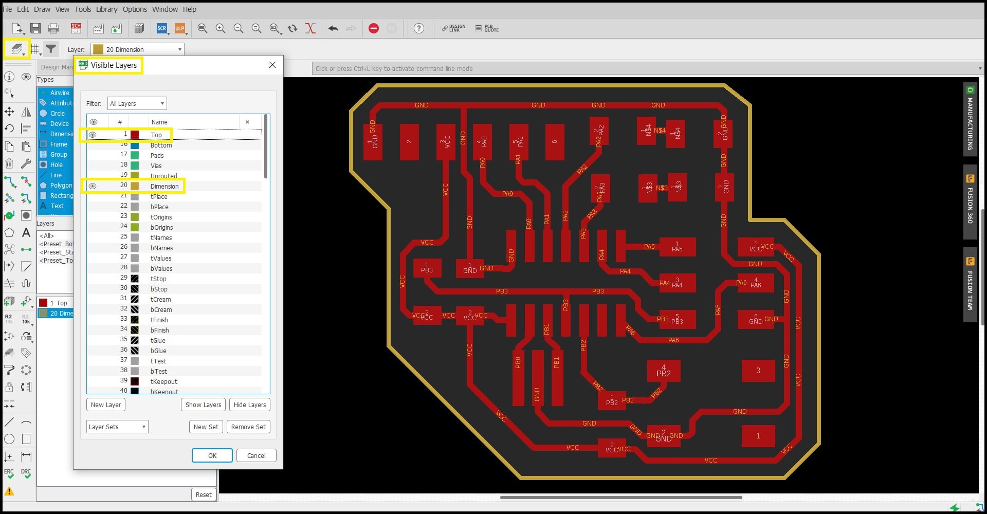
Step 4: Now we will draw a cutting lines around the board. Click on “Line” and then select layer “20 Dimension”. The cut lines will part of this layer. You can use straight lines and arcs.
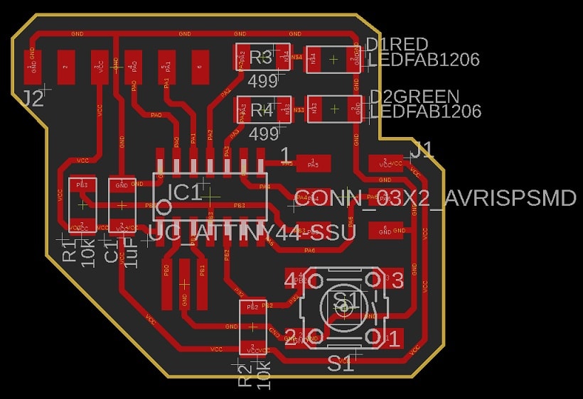
Step 5: Now we will export the traces and interiors as png files, so we can use in mods to generate the rml files for the milling machine. Go to “Layer Settings” and hide all layers by clicking on the eye icon, only keep “1 Top” and “20 Dimension”. Click “OK”.
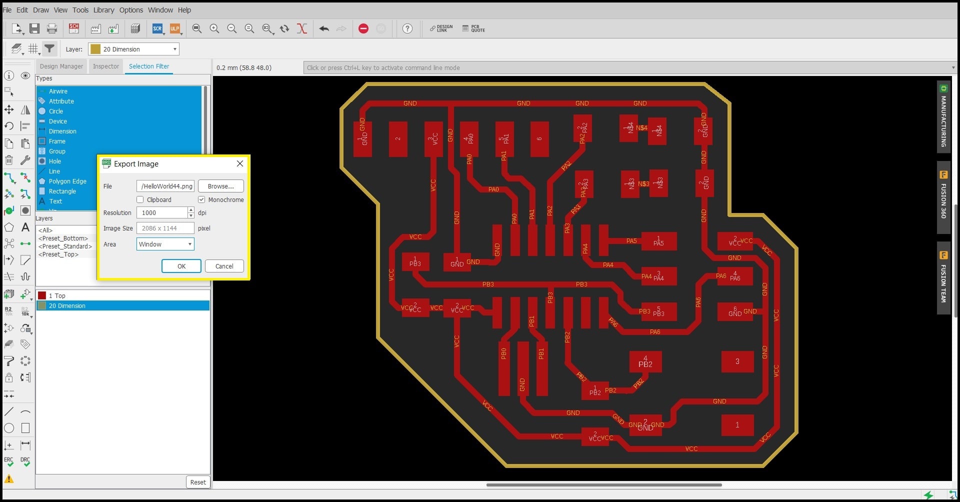
Step 6: Zoom you board to fit window. Go to “File > Export > Image”. Give your file a name, check “Monochrome”, set resolution to “1000 dpi” and set “Area” to “Window”. Click “OK”.
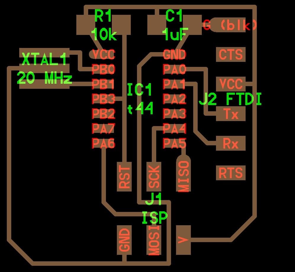
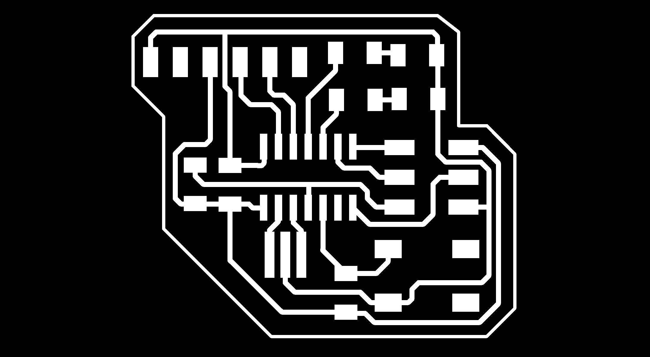
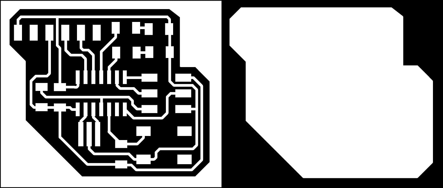
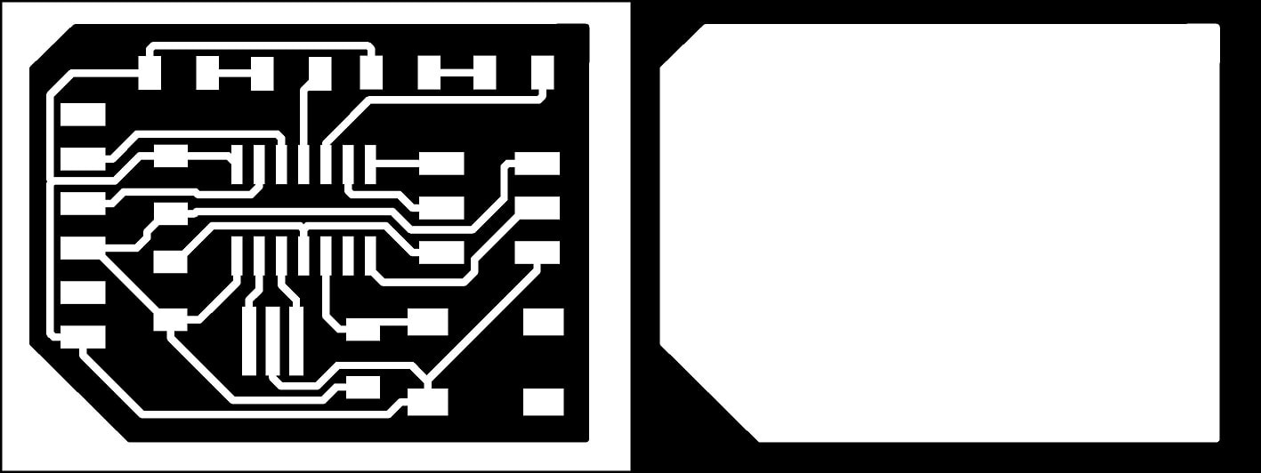
The exported image shown below.
Step 7: I used GIMP to crop the exported image. The dimensions of image after cropping will be the dimensions of PCB needed to make the board.
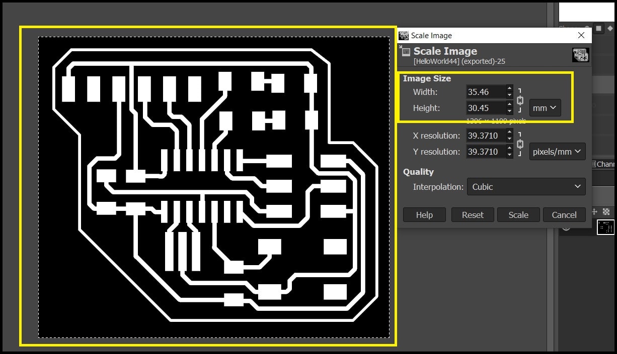
Step 8: Work on the cropped image to export two file; the traces and interiors. Then use mods to generate the rml files to make traces milling and interiors cuts.
Problems and Fixes
After working on mods, I examined the toolpaths and I noticed there were some traces still connected and not recognized by mods. To fix that, I increased the minimum spacing in design rules to 18 mils instead of 16 mils.
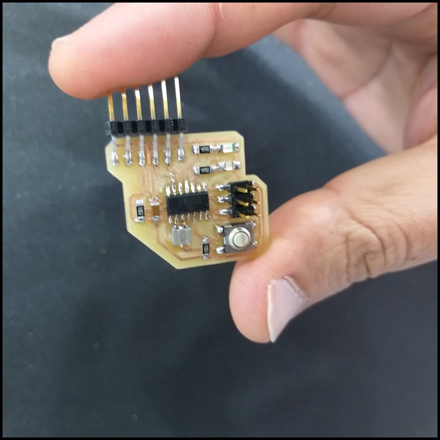
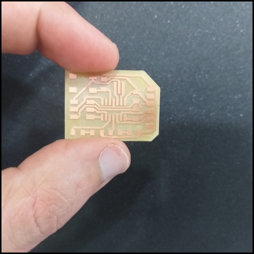
Hero Shoot!
Echo Hello-World Board Using KiCad
Software: KiCad
File Download
KiCad Fab library (fab.lib)
KiCad fab.pretty footprint library
KiCad echo hello-world ATtiny44 ZIP file
KiCad echo hello-world ATtiny44 board traces png file
KiCad echo hello-world ATtiny44 board interiors png file
KiCad echo hello-world ATtiny44 board traces rml file
KiCad echo hello-world ATtiny44 board interiors rml file
“KiCad (pronounced “Key-CAD”) is a free software suite for electronic design automation (EDA). It facilitates the design of schematics for electronic circuits and their conversion to PCB designs.” (Source).
In this part I redrew the echo hello-board using KiCad and added two LEDS and a push button.
Redrawing the Echo Hello-World board
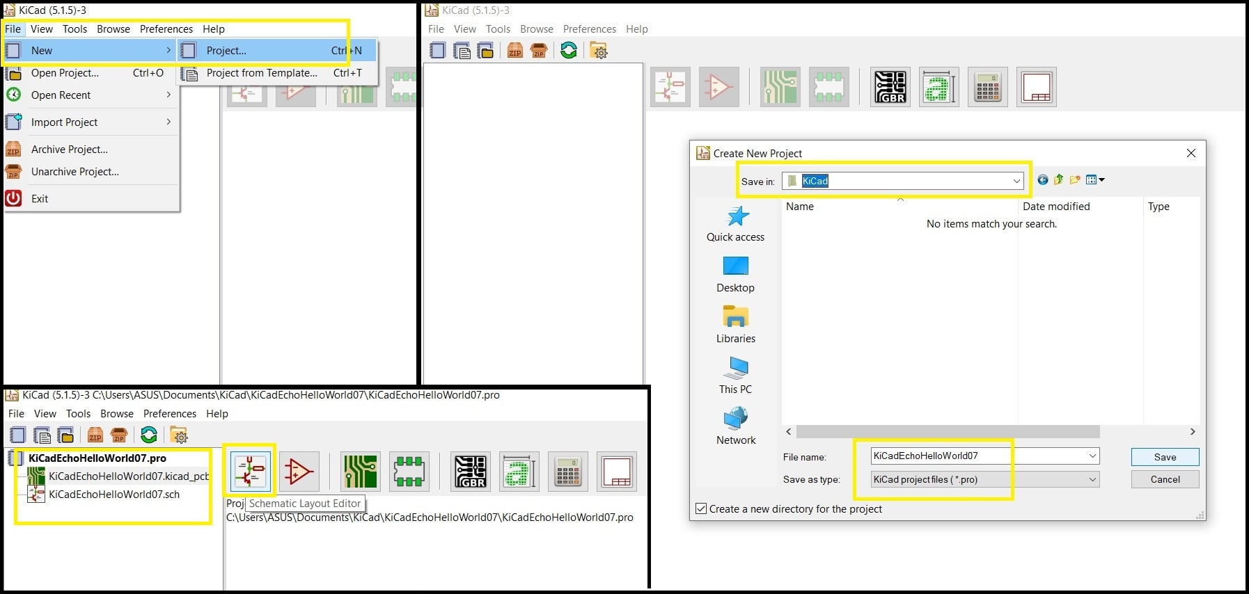
Step 1: Open KiCad software. Go to “File > New > Project”. Select the location and give your project a name. Click “Save”. I named mine “KiCadEchoHelloWorld07”. This will be the container for the schematic and PCB.
Step 2: Click on “Schematic Layout Editor”. A new window will open where we will make the schematic.
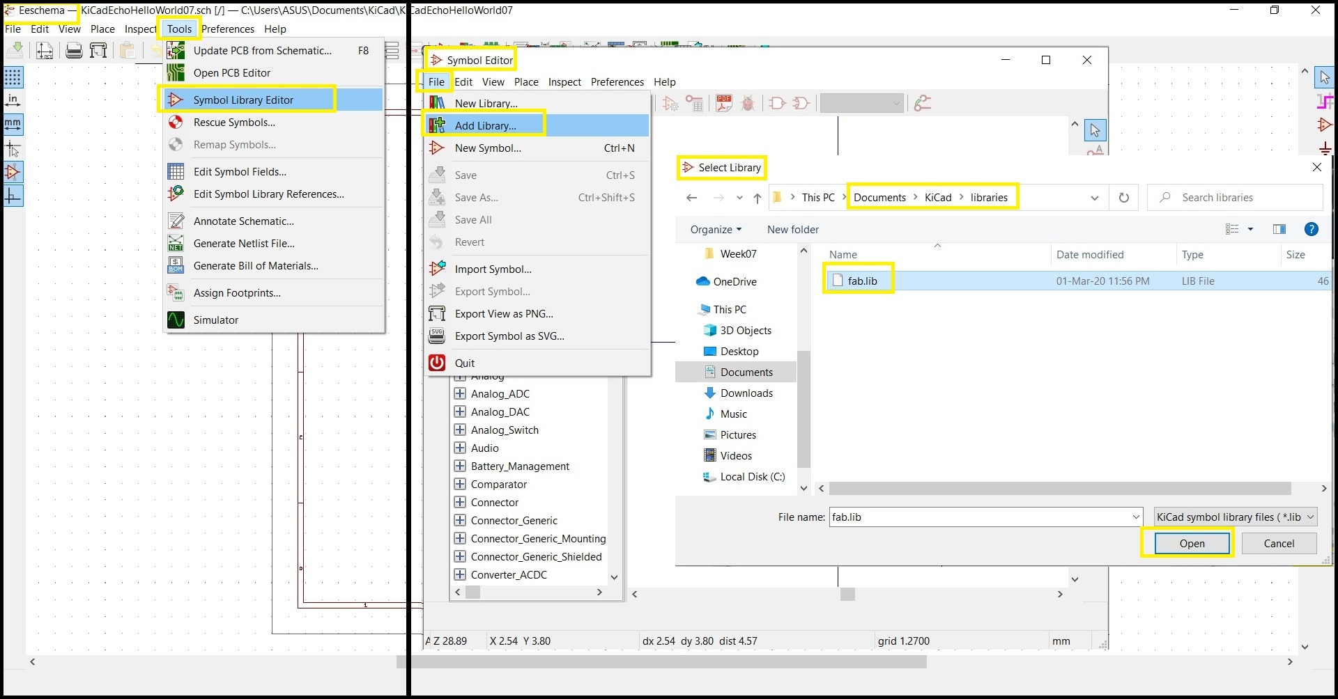
Step 3: First we will add Eagle fab library (fab.lib). Download the file and unzip it. I unzipped it in “..\Documents\KiCad\libraries”.
In Schematic Layout Editor go to “Tools > Symbol Library Editor”. A “Symbol Editor” Window will open. In symbol editor window go to “file > Add Library”. Locate fab.lib on your drive and click “Open”. Choose if you want this library to be for all projects “Global” or project specific “Project”. Now components in fab.lib are available to use.
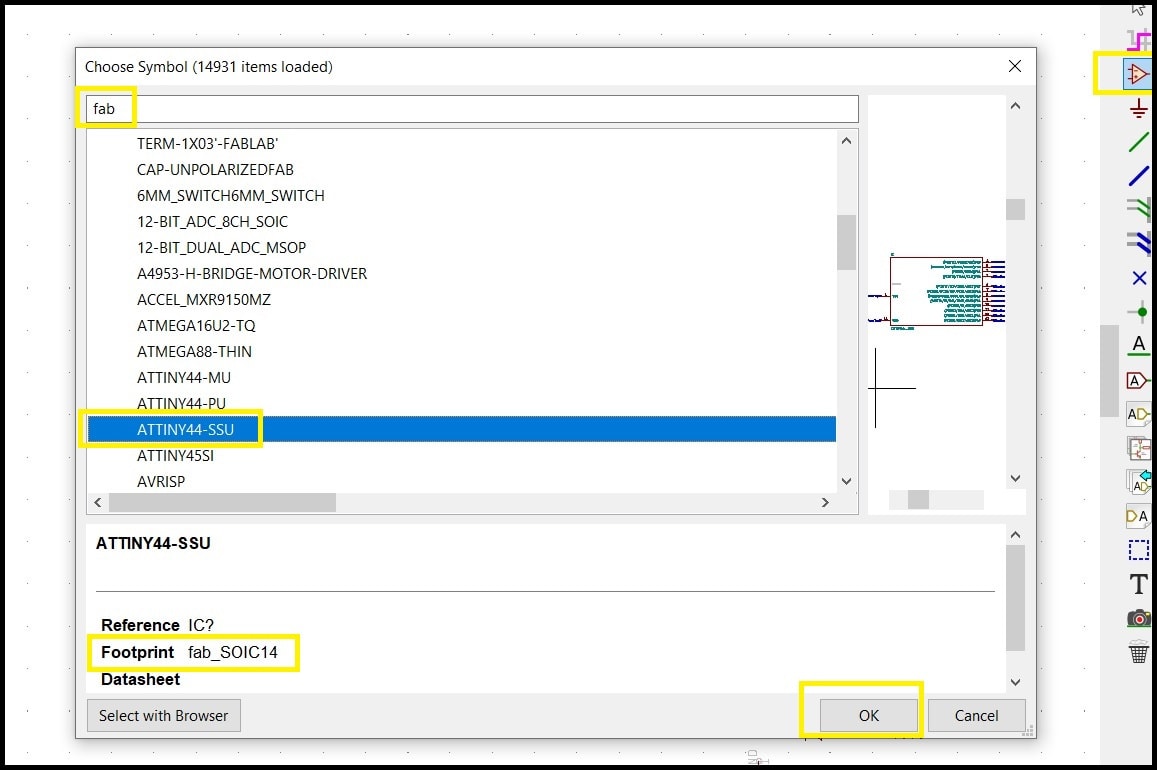
Step 4: Now we will add the components for the original echo hello-world ATtiny44 board. Click on “Place Symbol” and click any place in the work area. This will open “Choose Symbol” window. In “Filter” field type “fab”. Scroll down and click on “ATTINY44-SSU” and click “Ok”. Place the component any place in the work area. Repeat for all items in the table.
| Description | Reference | Lib Name | Qty |
|---|---|---|---|
| ATtiny44 | IC1 | ATTINY44-SSU | 1 |
| Crystal 20MHz | XTAL1 | RESONATOR | 1 |
| Header 3x2 ISP | J1 | AVRISPSMD | 1 |
| Header 1x6 FTDI | J2 | FTDI-SMD-HEADER | 1 |
| Capacitor unpolarized 1uF | C1 | CAP-UNPOLARIZEDFAB | 1 |
| Resistor 10kOhm | R1 | RES-US1206FAB | 1 |
Step 5: Add components in table below to the original echo hello-world ATtiny44 board. Work through the same steps to add to schematic. Remember to save your schematic. Add “VCC” and “GND” to the schematic. Also, add “PWR_FLAG”. This is to tell the ERC where the power is coming from.
| Description | Reference | Lib Name | Qty |
|---|---|---|---|
| Resistor 10kOhm | R2 | RES-US1206FAB | 1 |
| Resistor 499Ohm | R3, R4 | RES-US1206FAB | 2 |
| Green LED | D1 | LEDFAB1206 | 1 |
| Red LED | D2 | LEDFAB1206 | 1 |
| Push button | S1 | 6MM_SWITCH6MM_SWITCH | 1 |
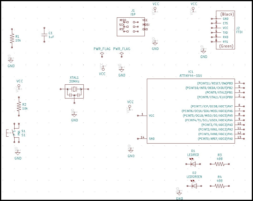
Step 6: For each component, right click and select “Properties > Edit Properties”, or you can move the mouse over the component and press “E”. Change reference and value. Your schematic should look similar to the image below.
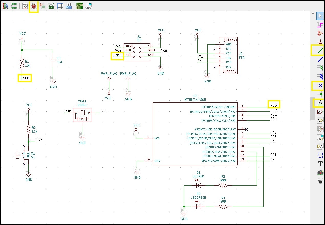
Step 7: As per the original echo hello-world ATtiny44 board and using “Place Wire” tool, add wiring to components. Make direct connections between components when possible. Using “Place net label” tool add labels to open connections. Using labels makes schematic less messy and works the same as direct connection between components. For example all open connections named “PB3” are connected together. A “Place no connection flag” should be used on pins that are not connected.
Run the “Perform electrical rule check”, you should have no errors.
Making the PCB
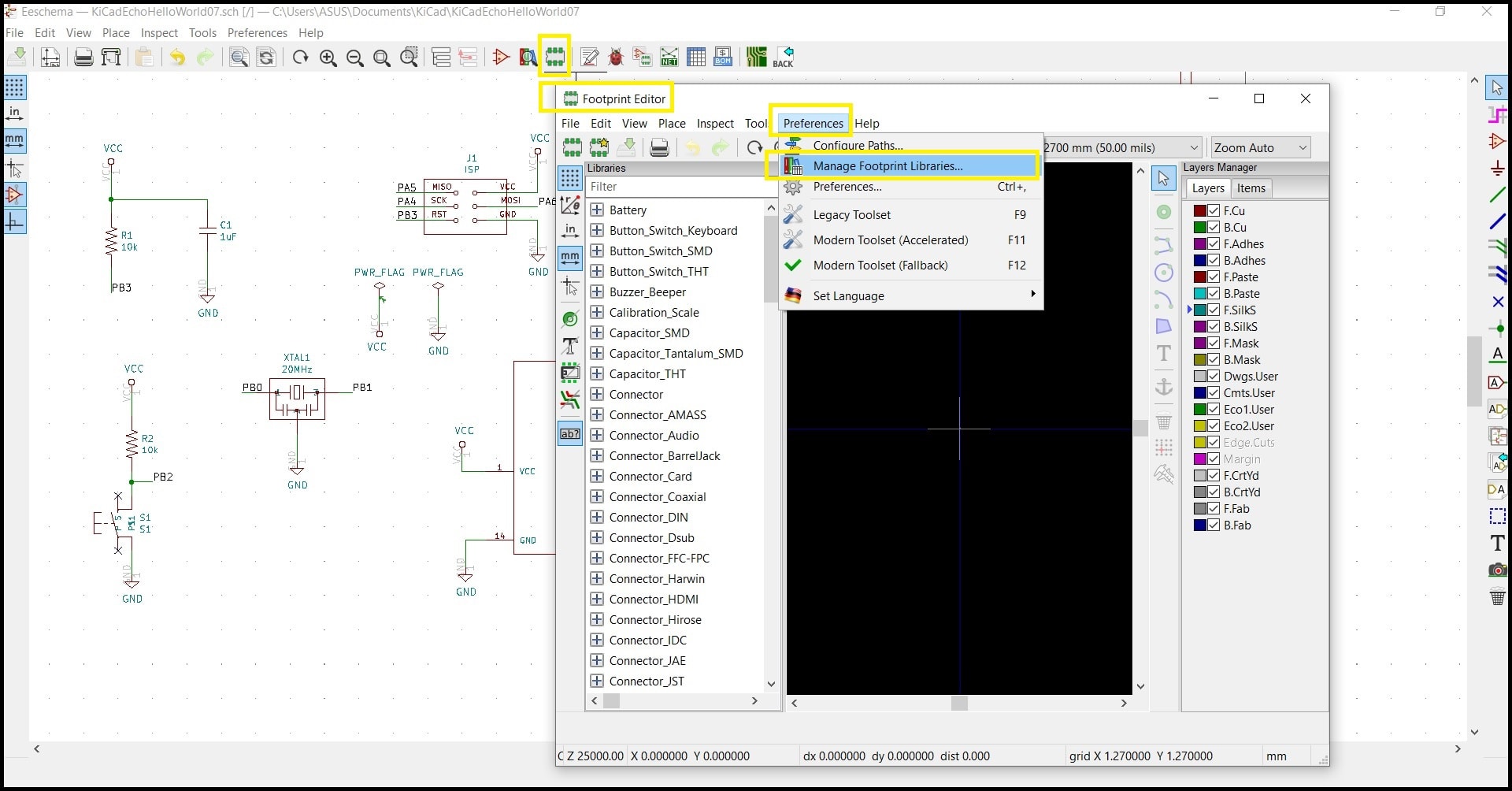
Step 1: Before we continue to PCB, we need to update the footprint for components in fab.lib. Footprints define the package of components used in PCB.
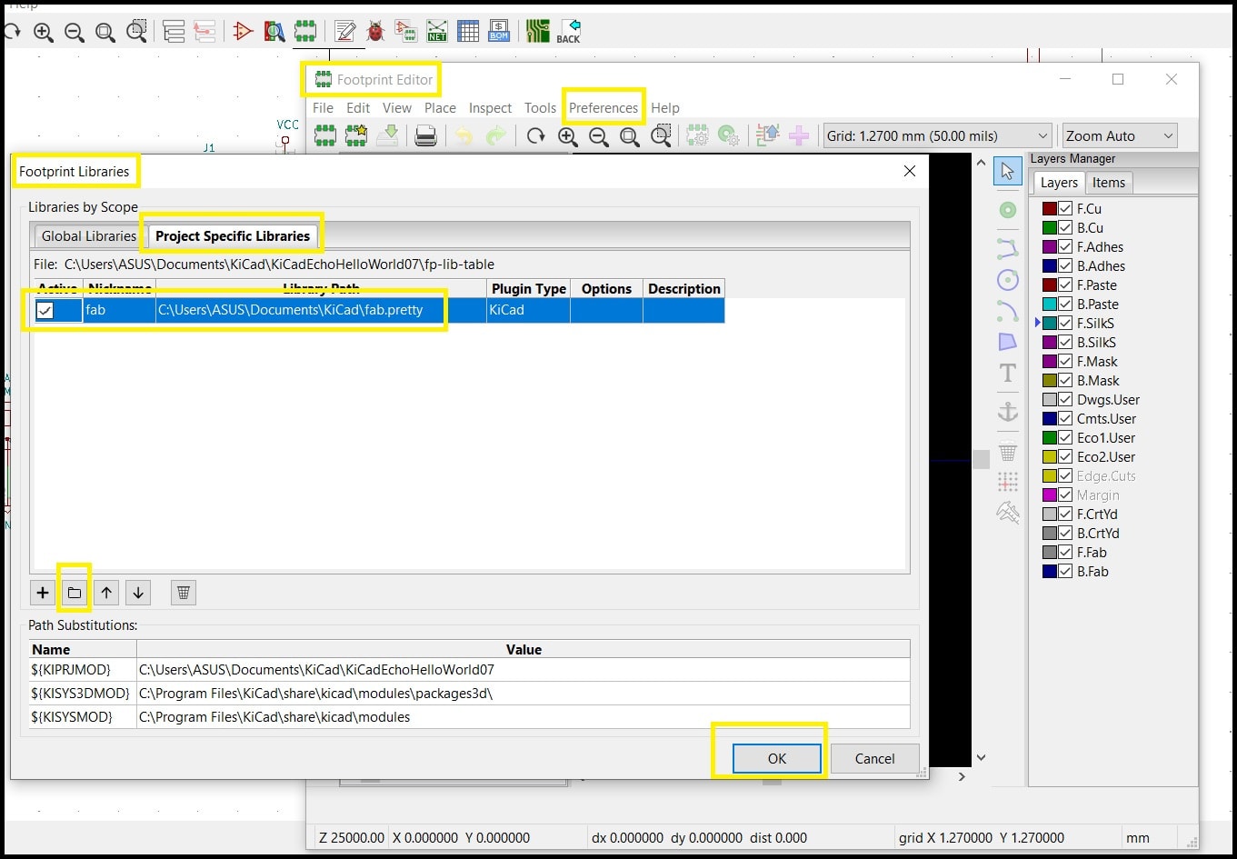
Download “KiCad fab.pretty footprint library” and unzip it. The footprints are save in folder “fab.pretty”. I saved it to “..\Documents\KiCad”. From schematic layout editor go to “Footprint Editor” and a new window will open. In footprint editor click on “preferences > Manage Footprint Libraries”.
Step 2: In “Footprint Libraries” select “Project Specific Libraries” if you only want to add the footprints libraries to this project. Click on “Add existing library to table” and locate your fab.pretty folder. Click “OK” and then “OK” for footprint libraries. Close the footprint editor.
Step 3: Now we are ready to work on the PCB. Go to schematic layout editor and click on “Assign PCB footprints tp schematic symbols”. If you receive a confirmation message click “No”. In “Footprints Libraries” tab select “fab” and then select “Filter footprint list by library”. This will load footprints only in fab library.
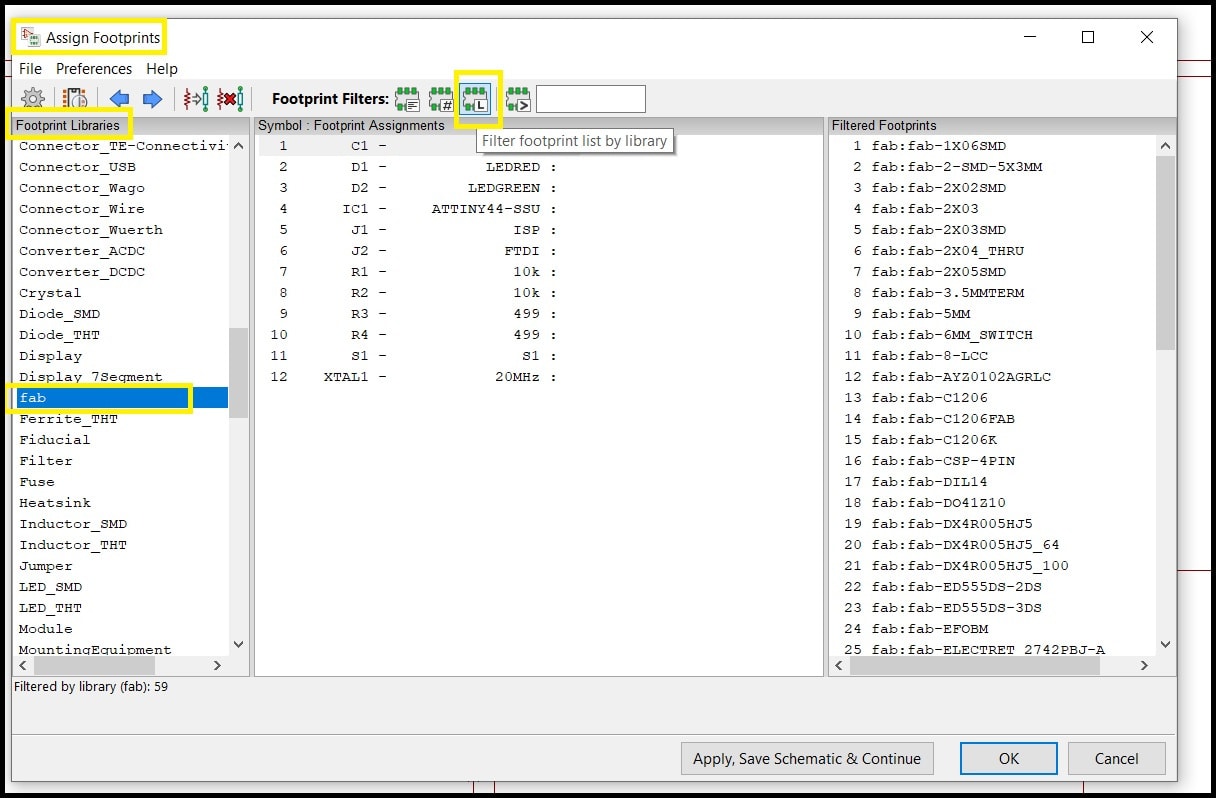
Step 4: Here we will assign a footprint to each component in our schematic, so PCB will update according to assigned footprints. The table below shows the footprint should be used for each component.
| Description | footprints |
|---|---|
| ATtiny44 | fab-SOIC14 |
| Crystal | fab-EFOBM |
| Header 3x2 ISP | fab-2X03SMD |
| Header 1x6 FTDI | fab-1X06SMD |
| Capacitor unpolarized | fab-C1260FAB |
| Resistors | fab-R1206FAB |
| LEDS | fab-LED1206FAB |
| Push button | fab-6MM_SWITCH |
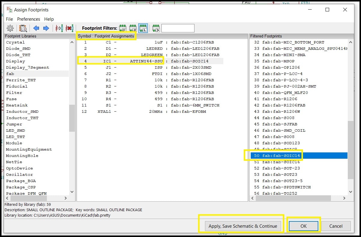
Select the “ATTINY44-SSU” from the “Symbol: Footprint Assignments” tab, and then double click “fab-SOIC14” from “Filtered Footprints” tab. Now the fab-SOIC14 footprint is assigned to ATtiny44. Repeat for all components. Click on “Apply, Save Schematic & Continue” and the click on “Ok”.
Step 5: In schematic layout editor, go to “Tool > Update PCB from Schematic”. A new window will open. Click “Update PCB” in the message shows and then “Close”. Click to place your board and click again any place in working area. Your board is a part of “F.Cu” layer.
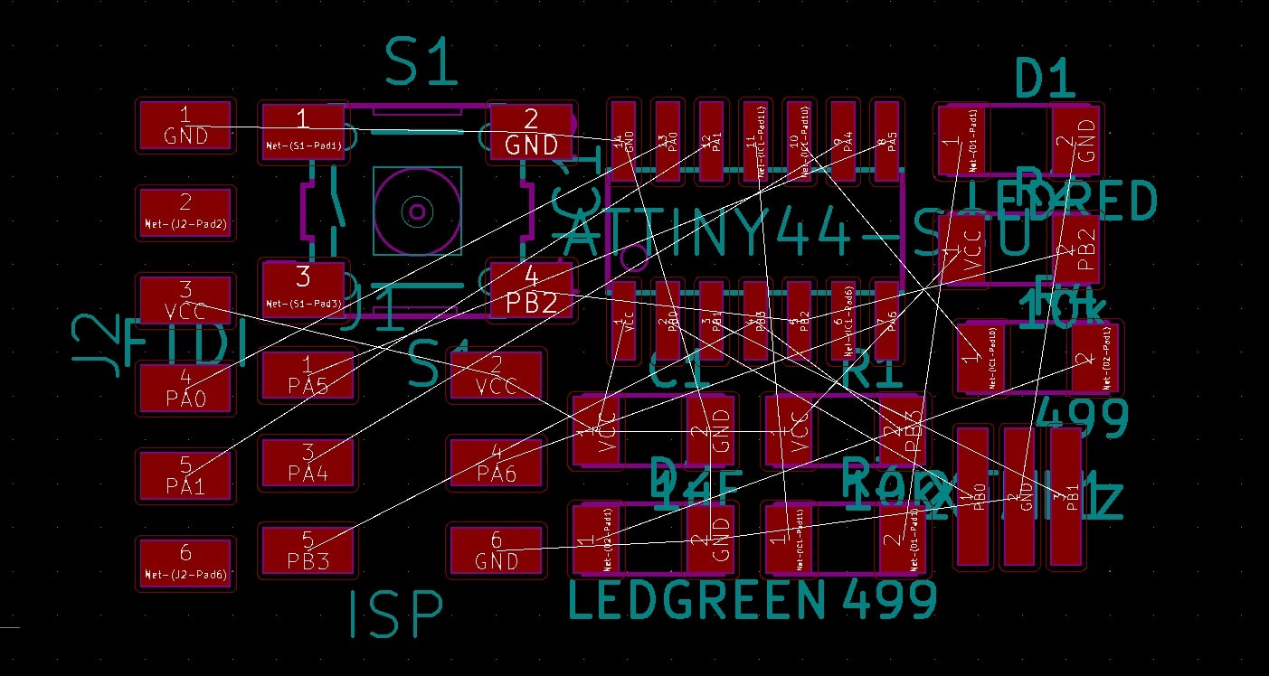
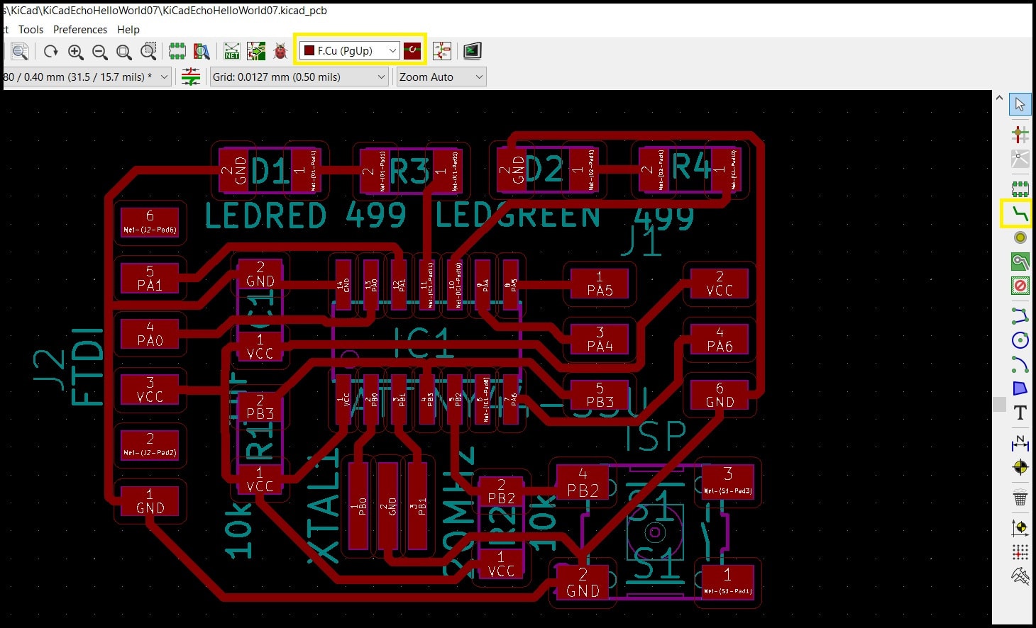
Step 6: Fine yellow wirings represent the connections made in the schematic. All those wirings should be replaced using “Route tracks” tool.
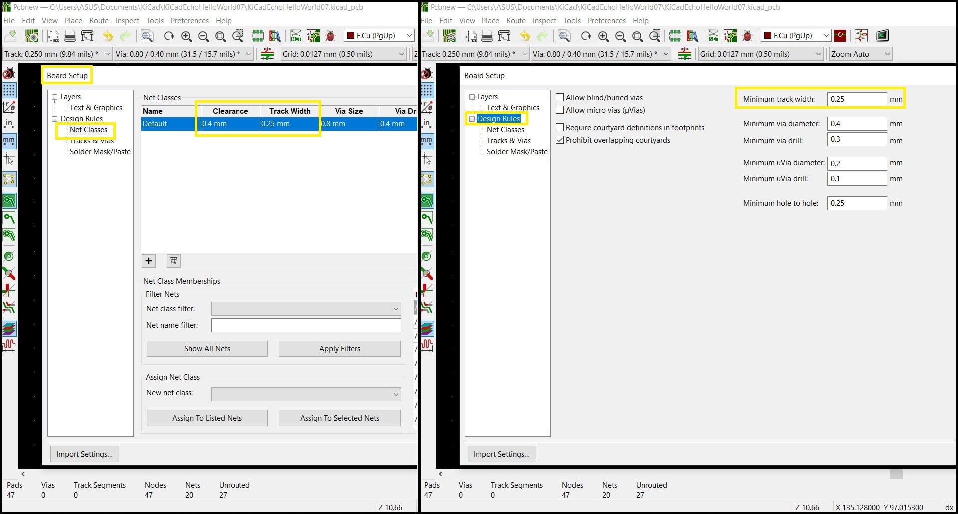
Before we start we need to define our design rules. In “Board Editor” go to “File > Board Setup”. Select “Net Classes” tab and change “Clearance = 0.41 mm” and “Track Width = 0.254 mm”. Now go to “Design Rule” tab and change “Minimum track width = 0.254 mm”. Click “Ok”.
Step 7: Use “Route tracks” tool to replace fine yellow connections and route between your components. You may take some time to find a good positioning for components. Route width is defined 0.254 mm and spacing between routes 0.41 mm to fit with 1/64” milling bit. Note that all routes are part of layer “F.Cu”.
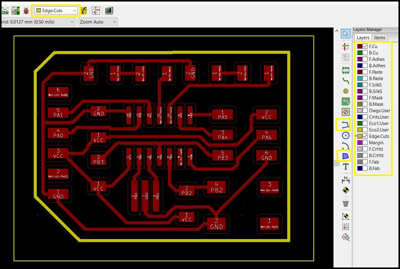
Step 8: Go to “Edge.Cuts” layer and using “Add graphic lines” tool, draw the cut lines for your board. Using “Add graphic polygon” tool, draw a polygon around the board. Start at the first corner and draw a polygon and end drawing by double click where you started.
Remove visibility for all layers, only keep “F.Cu” and “Edge.Cuts”.
Click on “Perform design rules check” and then “Run DRC” to see if there are any errors or warnings in your board.
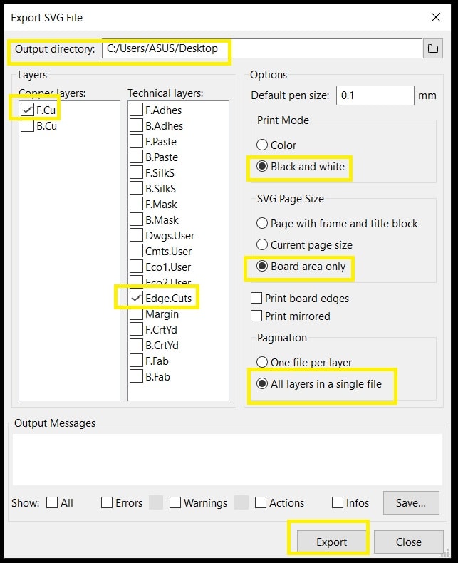
Step 9: Now we will export the board as SVG file. Go to “File > Export > SVG…” and use the settings below.
Step 10: Open the SVG file using GIMP and set “Resolution” to 1000 pixel/in. Crop the image if necessary and work to export traces and interiors. The image or cropped image dimensions are the dimensions of PCB needed to make the board.
Use mods to generate the rml files to make traces milling and interiors cuts.
Problems and Fixes
After working on mods, I examined the toolpaths and I noticed there were some traces still connected and not recognized by mods. To fix that, I increased the minimum spacing in design rules to 18 mils instead of 16 mils.
Hero Shoot!
Testing The Board
File Download
hello.ftdi.44.echo.c C file
hello.ftdi.44.echo Makefile
Step 1: Download the C and Makefile. Save to your computer and change the name of the makefile to “Makefile”.
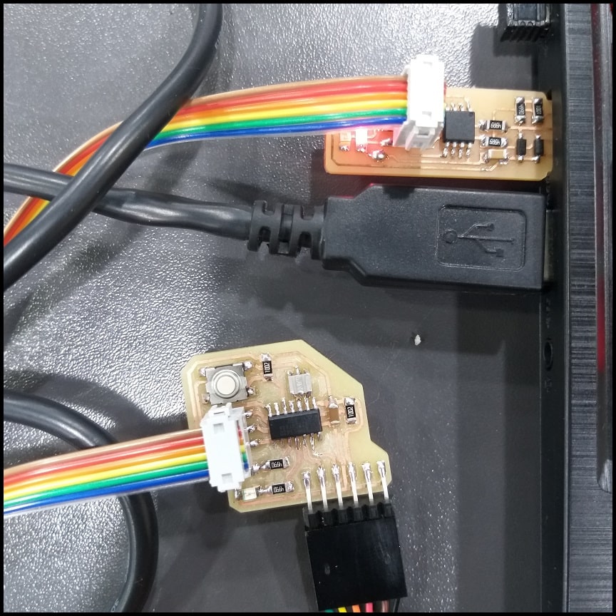
Step 2: Connect the board to FabTiny programmer through the SPI cable. Connect the FTDI cable to the board through FTDI header. Make sure that you connect cables in the right direction such that the board, SPI cable and FTDI cable have the same GND. Connect the programmer and the FTDI cable to USB ports.
Step 3: Run “Git Bash” in the folder where you saved the C and makefile. In git bash window, execute “Make” to generate the HEX file which will be uploaded to board.
Step 4: In git bash window, execute “make program-usbtiny-fuses”. This will program the ATtiny44 fuses.
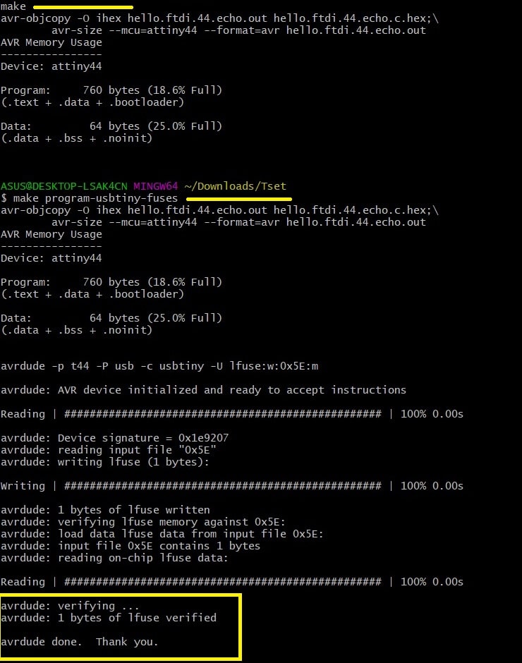
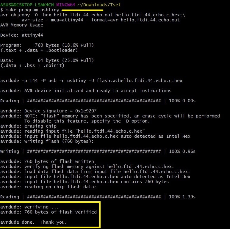
Step 5: In git bash window, execute “make program-usbtiny”. This will upload the HEX to ATtiny44.
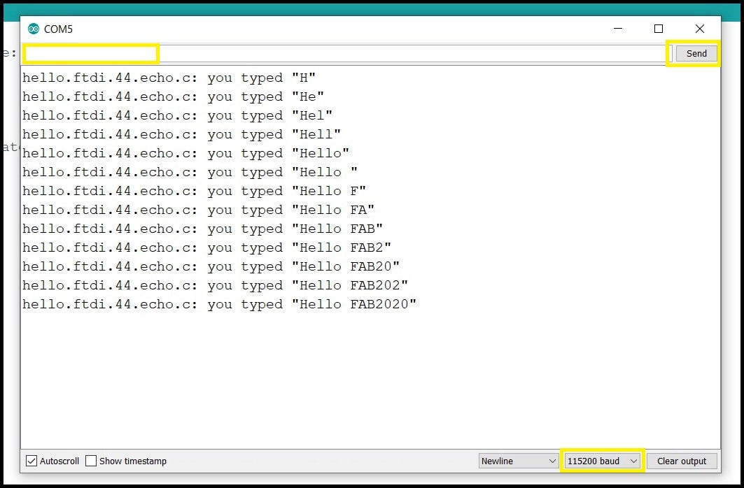
Step 6: I used “Arduino Serial Monitor” to test the program. Change the baud rate to “115200”, type a character and click “Send”. The board should echo back your input and print it back with a customized message. Input should be done character by character.
Hero Shoot!