5. Electronics Production
Group Assignment
PCB Desktop Milling Machine
File Download
Trace width test “traces” png file
Trace width test “traces” rml file
Trace width test “interiors” png file
Trace width test “interiors” rml file
Machine: Roland monoFab SRM-20
This part of the group assignment was about the Roland monoFab SRM-20 desktop milling machine. We used the machine to complete a trace width test on a single layer PCB.
The PCB
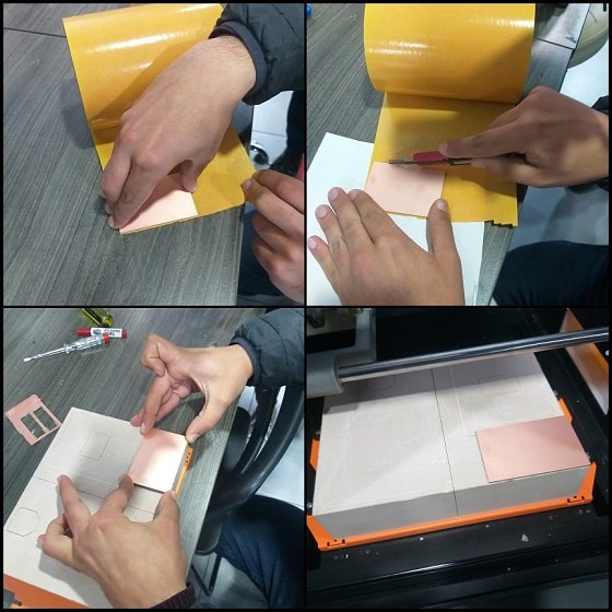
We used FR4 single layer PCB (laminate thickness = 1.2 mm, copper base thickness 0.1 mm). Using a utility knife, cut a piece little larger than the size of your design. Fix the cut piece on a thin double face tape and cut around it. Remove the lower paper of the double face and fix the board on the high density foam used in the machine.
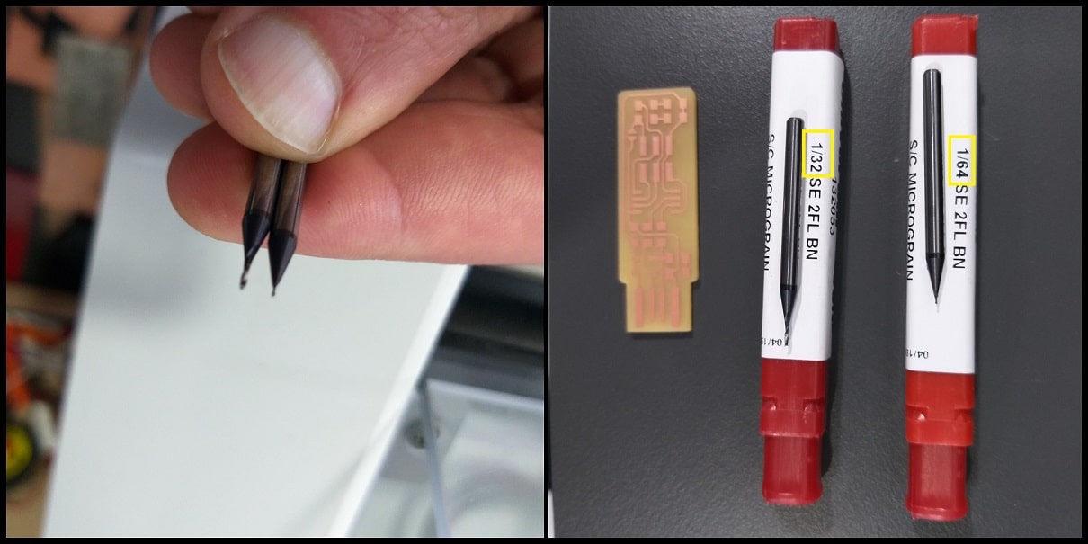
Milling Bits
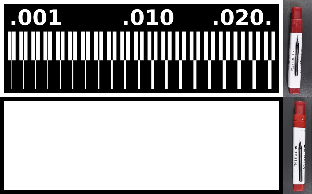
We used two milling bits; for traces 1/64” (0.4 mm), and for interiors 1/32” bit (0.8 mm).
mods
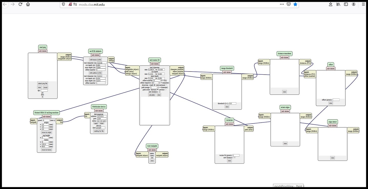
We used mods to generate the rml files from png images. The rml extension is the accepted format for the Roland machine. Job consists of two parts; First the milling of traces. For this part we used the traces png file and 1/64” (0.4 mm) milling bit. Second the cutting of the interior. For this part we used the interior png file and 1/32” (0.8 mm) milling bit.
Step 1: Open mods and right click to open the selection list. Click on programs > open server program > machines > Roland > mill > SRM - 20 > PCB png.
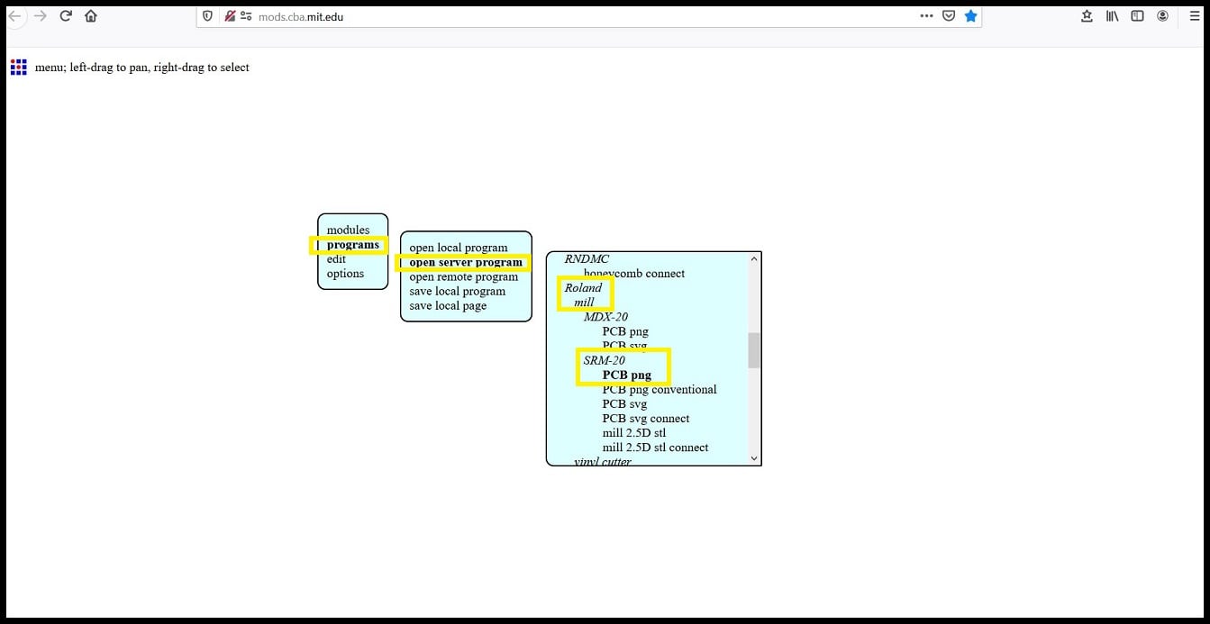
This action will open the program associated with our lab machine.
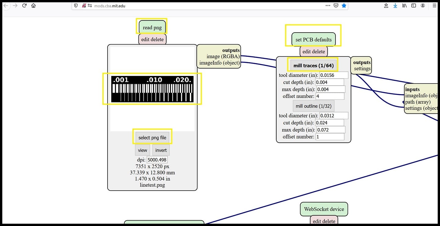
Step 2: Using the “read png” block in the program, click on “select png file” and select the traces png file.
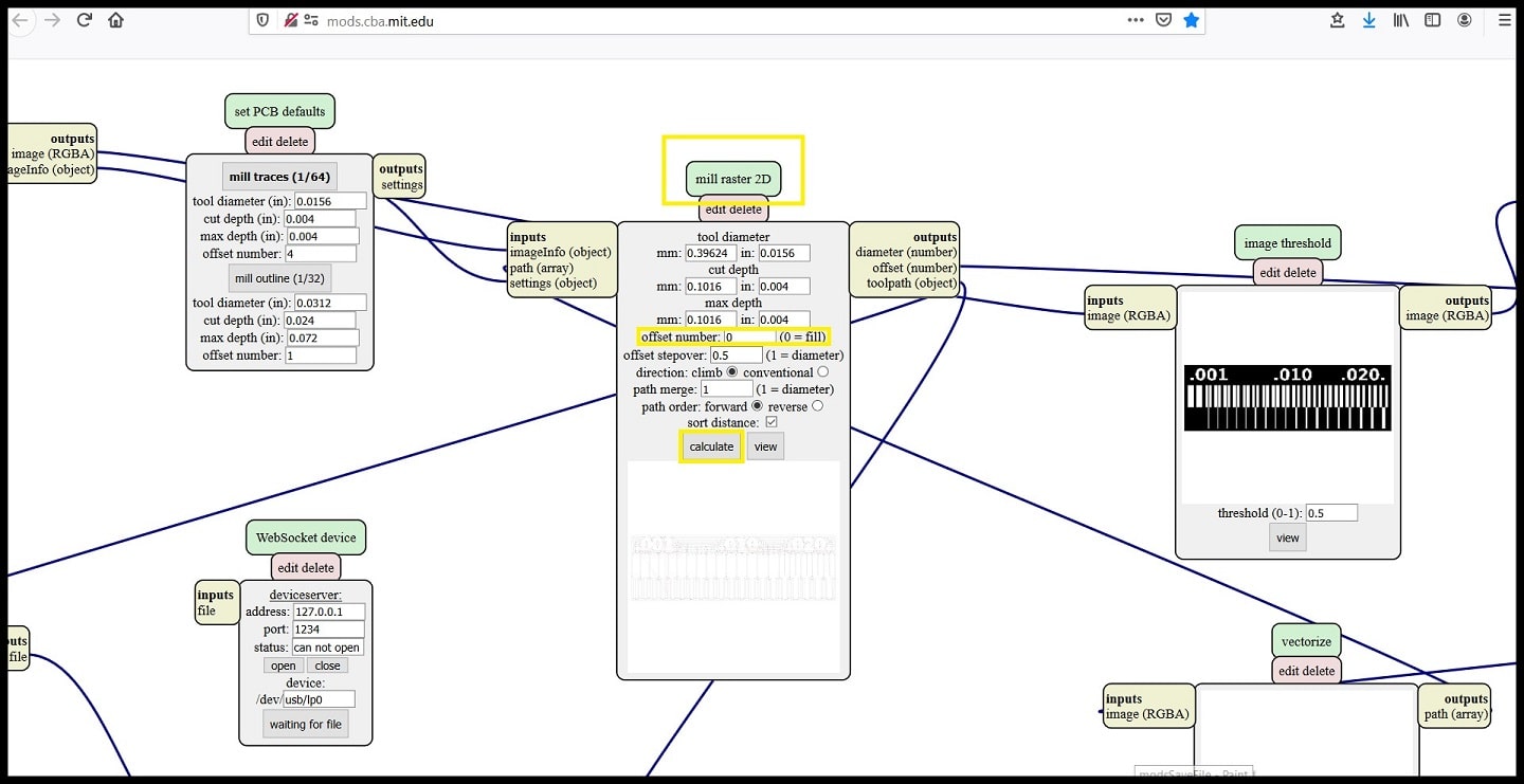
Step 3: On the “set PCB defaults” block, click on “mill trace (1/64)” to select the right milling bit. The copper base thickness of the FR4 PCB is 0.1 mm. “Cut depth” is set to 0.004” (0.1 mm). The “max depth” will control the repetition of milling over the same place. “Max depth” is set to 0.004” (0.1 mm), which means unwanted copper will be milled once, and that is enough since copper thickness is 0.1 mm. “Offset number” controls the milling spacing around traces. “Offset number” is set to 4, which means the spacing, where applicable, will be 4 times the bit width; 4 x 1/64” (0.4 mm) = 1/16” (1.6 mm). If “Offset number” is set to zero, all unwanted copper will be removed.
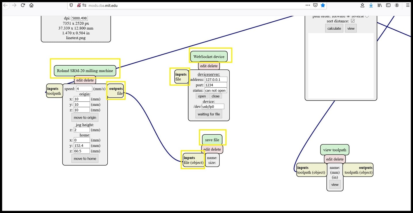
Step 4: The program is designed to communicate with the machine if operated in LINUX OS. The final output of the program will be sent to “WebSocket device”. I made a change and fed the output into “save file” module, so the rml file will be save locally and then used on the milling machine software.
To add a “save file” module, right click to open the selection list, click on modules > open server module > file > save .
Move the mouse over the output node of “Roland SRM-20 milling machine”, click when the word “file” becomes bold. Do the with the input node of “WebSocket device”. The connection between both should disappear. Again, move the mouse over the output node of “Roland SRM-20 milling machine”, click when the word “file” becomes bold. Do the with the input node of “save file” module. The connection between both should be established.
Step 5: In “mill raster 2D” block, change settings as your requirements. I changed “offset number” to 0 so all copper will be milled out and only traces will be left. Click on calculate and when the program finishes a dialog box will appear and ask you to save the file locally.
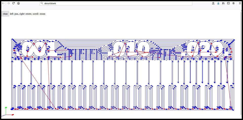
The image below shows the result tool path for traces file.
Step 6: Using the “read png” block in the program, click on “select png file” and select the interior png file.
Step 7: On the “set PCB defaults” block, click on “mill trace (1/32)” to select the right milling bit. The laminate thickness of the FR4 PCB is 1.2 mm. “Cut depth” is set to 0.024” (0.6 mm). The “max depth” will control the repetitions of cutting over the same lines. “Max depth” is set to 0.072” (1.8 mm), which means the same line will be cut 3 times; 0.072” / 0.024” = 3. This will ensure that our board will be separated from the parent board.
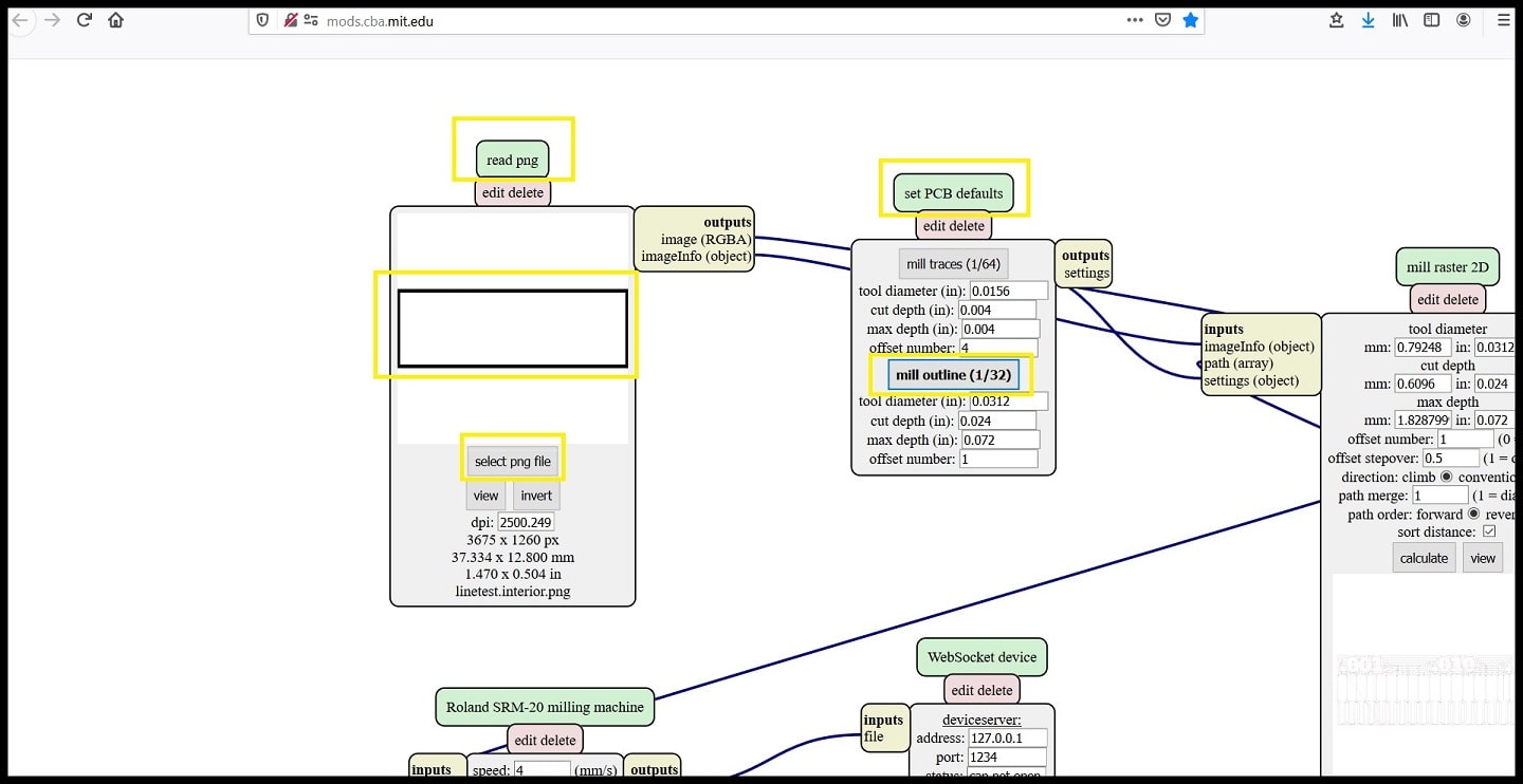
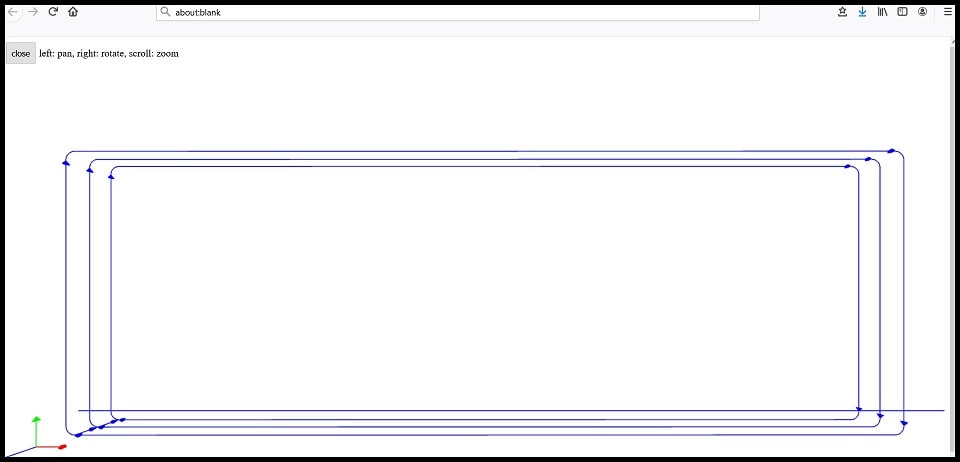
Step 8: In “mill raster 2D” block, click on calculate and when the program finishes a dialog box will appear and ask you to save the file locally. The image below shows the result tool path for interiors file.
VPanel for SRM-20 software
Now we are ready to use the rml files to mill and cut the board design. Before we start we need to define the origin of the mill bit by referencing its relative position.
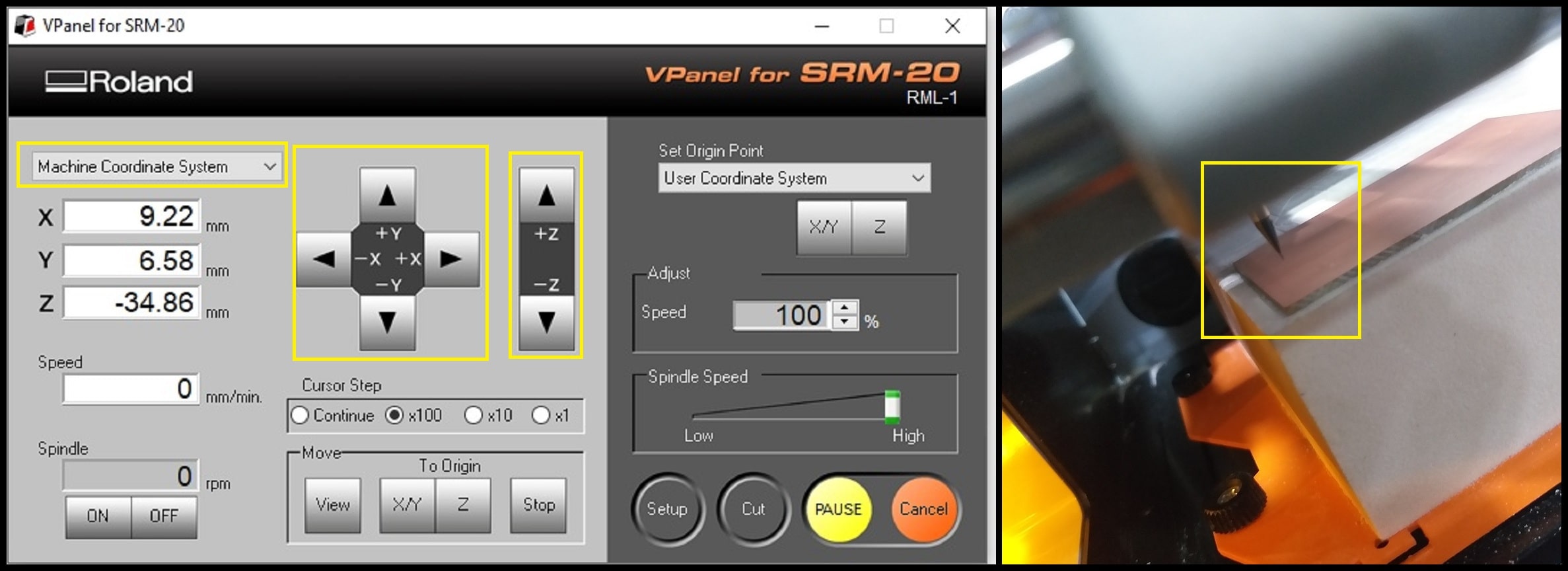
Step 1: Open the VPanel software and select “Machine Coordinate System” option from the dropdown menu.
Use the “+X, -X” and “+Y, -Y” arrows to move the head over the bottom left corner of the PCB. Use the “+Z” arrow to have enough space between the spindle and the PCB to insert the milling bit.
Step 2: Insert the 1/64” milling bit in the spindle collet leaving about 25% of its length outside. Tie the fixing screw.
Step 3: Using the “-Z” arrow, move the spindle down till there is about 5 mm between the PCB and milling bit tip. Hold the milling bit between your fingers and untie the fixing screw. Move the milling bit down till it touches the PCB. Tie the fixing screw firmly. This is your home position.
Step 4: From the “Set Origin Point” dropdown menu to the right, make sure to select “User Coordinate System”. Click on “XY” and “Z”. This will define the current position as the home or zero position in the user coordinate system. Select “User Coordinate System” from the dropdown menu to the left. The values of “X”, “Y”, “Z” should be zeros.
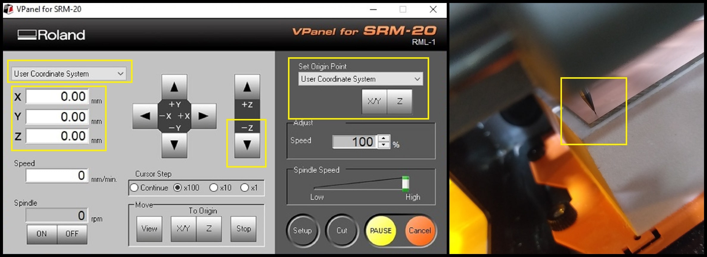
Step 5: Using the “+Z” arrow move the milling bit a few millimeters above the PCB, so that when the spindle starts it won’t be touching the PCB.
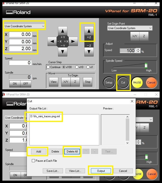
Step 6: Click on “Cut” and click on “Delete All” to remove any old jobs. Click on “Add” and select the traces rml file. Click on “Output”. The machine should start now.
Step 7: When the trace milling is complete, remove the 1/64” bit and click on “XY” in “Move” menu. This will move the spindle to “XY” home defined in user coordinate system. Replace the milling bit with the 1/32” bit. Change to “Machine Coordinate System” and follow the same procedure used when the bit 1/64” was used. Set origin point for the “Z” only and go back to “user Coordinate System”. For “X” and “Y” the origin point is the same defined for the traces milling. Complete the cut using the same steps for the traces file and using interior rml file.
The videos below shows traces milling and interior cutting.
Hero Shoot!
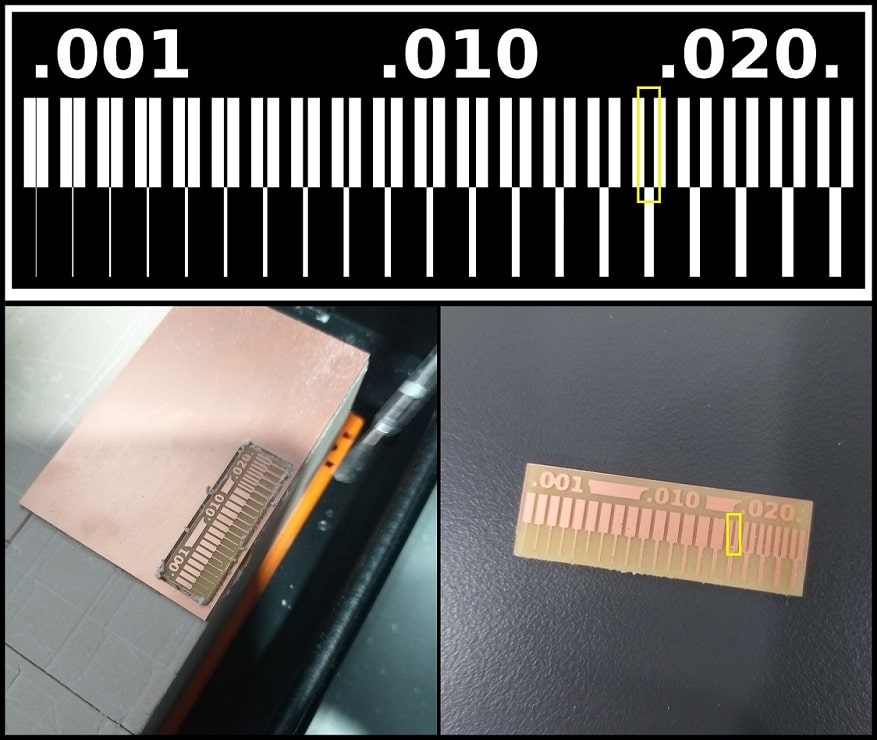
The milling bit used for traces (1/64”) couldn’t complete traces less than 0.016”. This is expected, since the size of the milling bit is 0.0156” (1/64”), it cannot be used to complete trace width less than that value.
Week Assignment
The FabTiny ISP
File Download
FabTiny ISP “traces” png file
FabTiny ISP “traces” rml file
FabTiny ISP “interiors” png file
FabTiny ISP “interiors” rml file
ATtiny45 datasheet
Atmel AVR Toolchain for Windows ZIP file
GNU Make installer
avrdude ZIP file
Zadig exe file
Firmware Source Code ZIP file
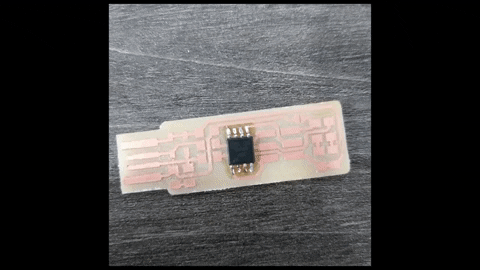
The FabTiny ISP is used to program other AVRs. The core of the FabTiny ISP is the ATtiny45 Atmel Microcontroller. After making the PCB and soldering the components, it should be programmed once and then it could be used as ISP programmer.
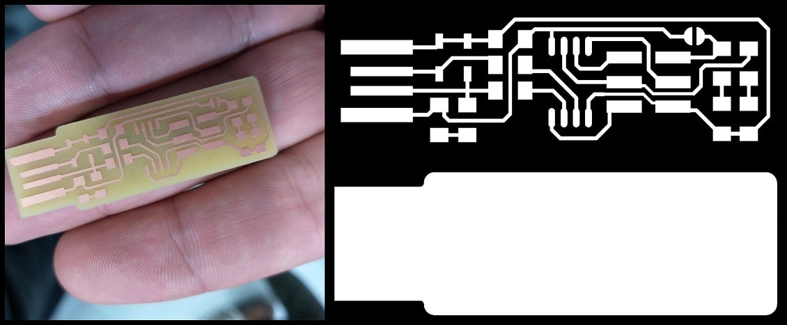
The PCB
Download the png files for the ISP traces and interior. If you are using the same machine (Roland monoFab SRM-20), you can download the rml file and use them.
I followed the same steps described in section “VPanel for SRM-20 software” in group assignment and made my FabTiny ISP PCB. For “offset number” I put 0 to remove all copper and keep only traces.
FabTiny ISP Schematic
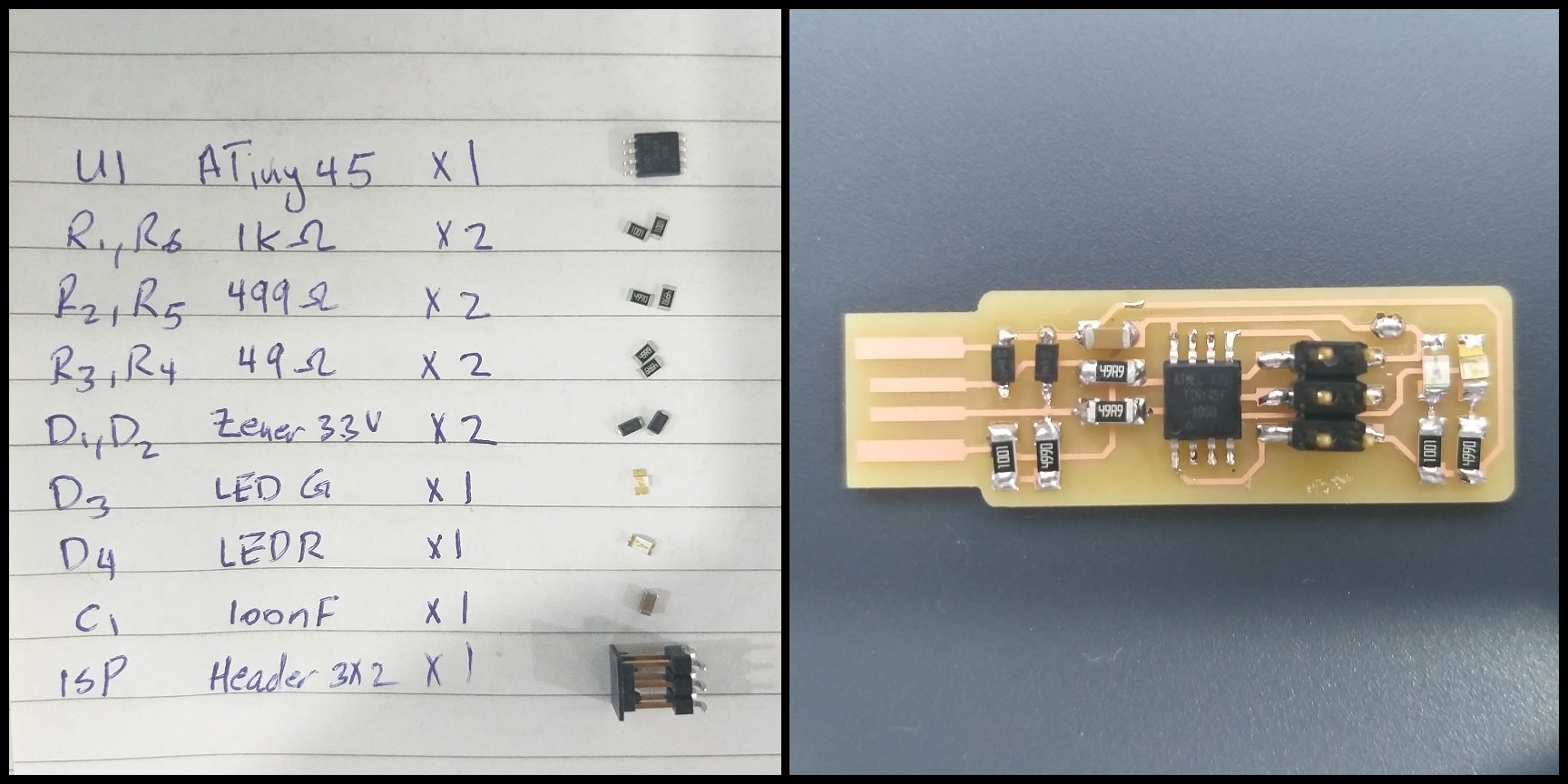
Below is the schematic of FabTiny ISP PCB. From this schematic I listed components needed to complete the ISP. Note that all components are SMDs.
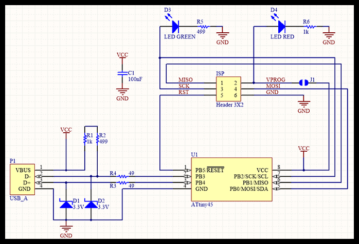
| Description | Reference | Quantity |
|---|---|---|
| ATtiny45 | U1 | 1 |
| Resistor 1 kOhm | R1, R6 | 2 |
| Resistor 499 Ohm | R2, R5 | 2 |
| Resistor 49 Ohm | R3, R4 | 2 |
| Zener diode 3.3 V | D1, D2 | 2 |
| Green LED | D3 | 1 |
| Red LED | D4 | 1 |
| Capacitor 100 nF | C1 | 1 |
| Header 3x2 | ISP | 1 |
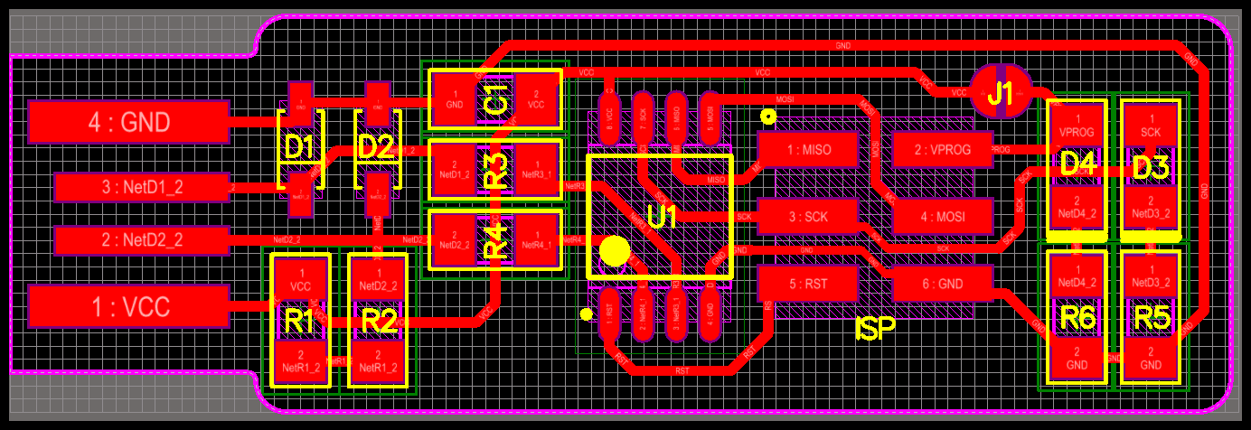
FabTiny ISP Soldering
Using component references and board image below, I completed soldering the ISP. I started with the inner component (ATtiny45) and moved out working on small components first.
Step 1: Using soldering iron and soldering wire, put a small amount of solder on copper where one of the ATtiny45 should be placed, let it be pin 8.
Step 2: Using tweezers, hold the ATtiny45 and place in the right position and orientation.
Step 3: Using soldering iron, heat solder point you put in step 1 till it melts. Keep the ATtiny45 in place till solder solidifies again. This will keep the ATtiny45 in the right position. Work on other pins.
Development Environment (Windows 10)
In order to program the FabTiny ISP target board, suitable tools and drivers should be installed to environment (Windows 10) to correctly identify and work on the programmer, and then can use on the FabTiny ISP target board.
You can use Linux, MacOS or Windows to program you board to become a programmer. Thanks to Brian Mayton for the great tutorial and step by step instructions.
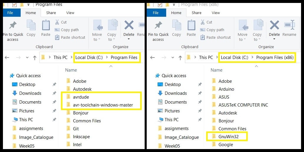
Step 1: Download “Atmel AVR Toolchain for Windows” ZIP file. Extract it and copy the folder “avr-toolchain-windows-master” to “C:\Program Files”.
Step 2: Download “GNU Make” installer file and launch it. Proceed with default installation options.
Step 3: Downlaod “avrdude” ZIP file. Extract it and copy the folder “avrdude” to “C:\Program Files”.
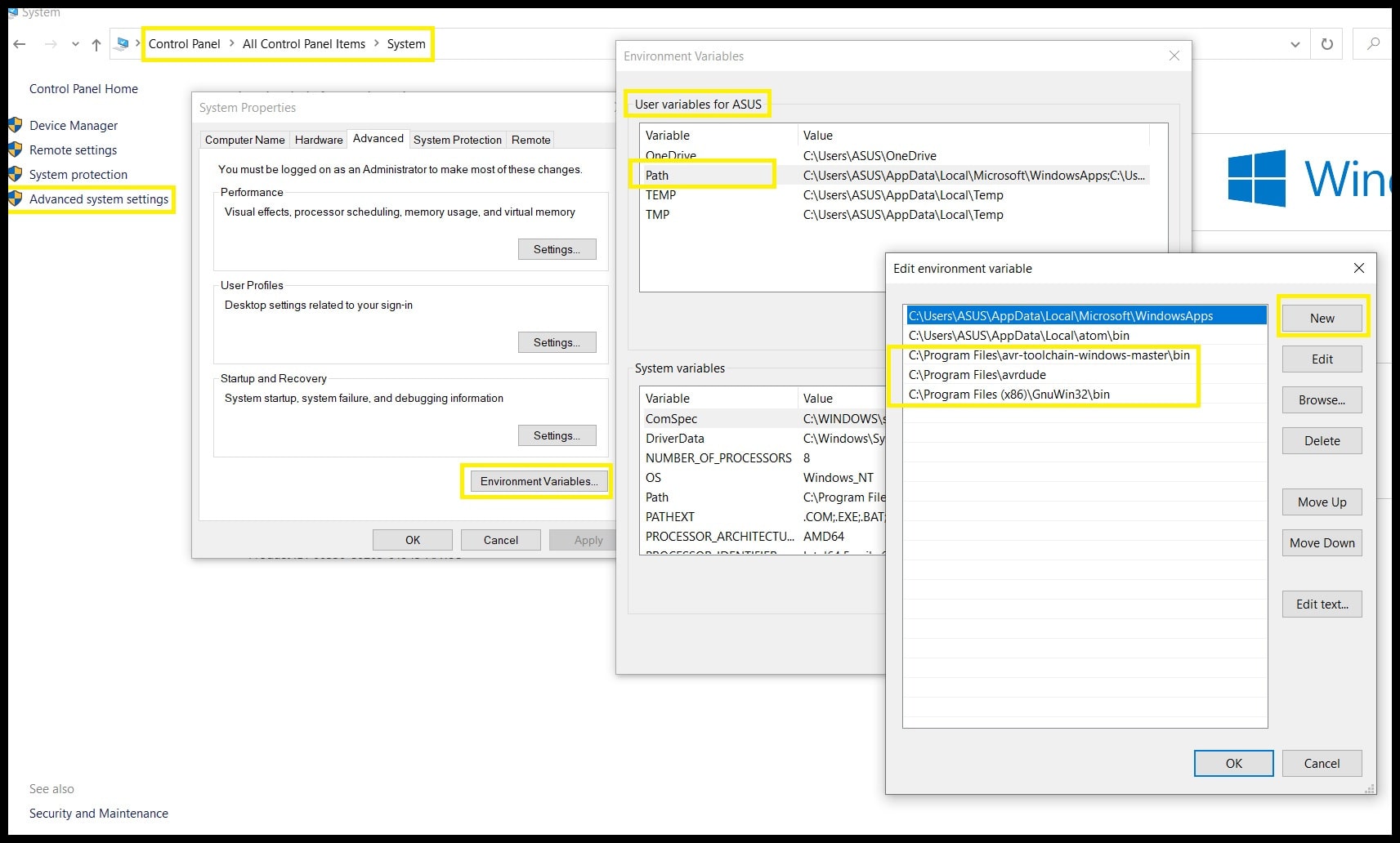
Step 4: Open Control Panel > System > Advanced System Settings > Environment Variables and in “User Variables” section select “Path” and click on “Edit”. For each path listed below click on “New” and add it to the list.
C:\Program Files\avr-toolchain-windows-master\bin
C:\Program Files (x86)\GnuWin32\bin
C:\Program Files\avrdude
This will tell Windows where the locations are for the tools when used in Git Bash command line.
Step 5: Downlaod “Zadig” and run it. Insert the programmer into USB and go to Zadig > Options > List All Devices. Select “USBtinySPI” from the dropdown list and select “libusb-win32 (v1.2.6.0)” in the target driver side. Click on “Install Driver”
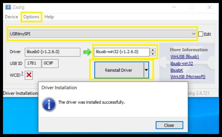
The programmer should be now recognized by Windows.
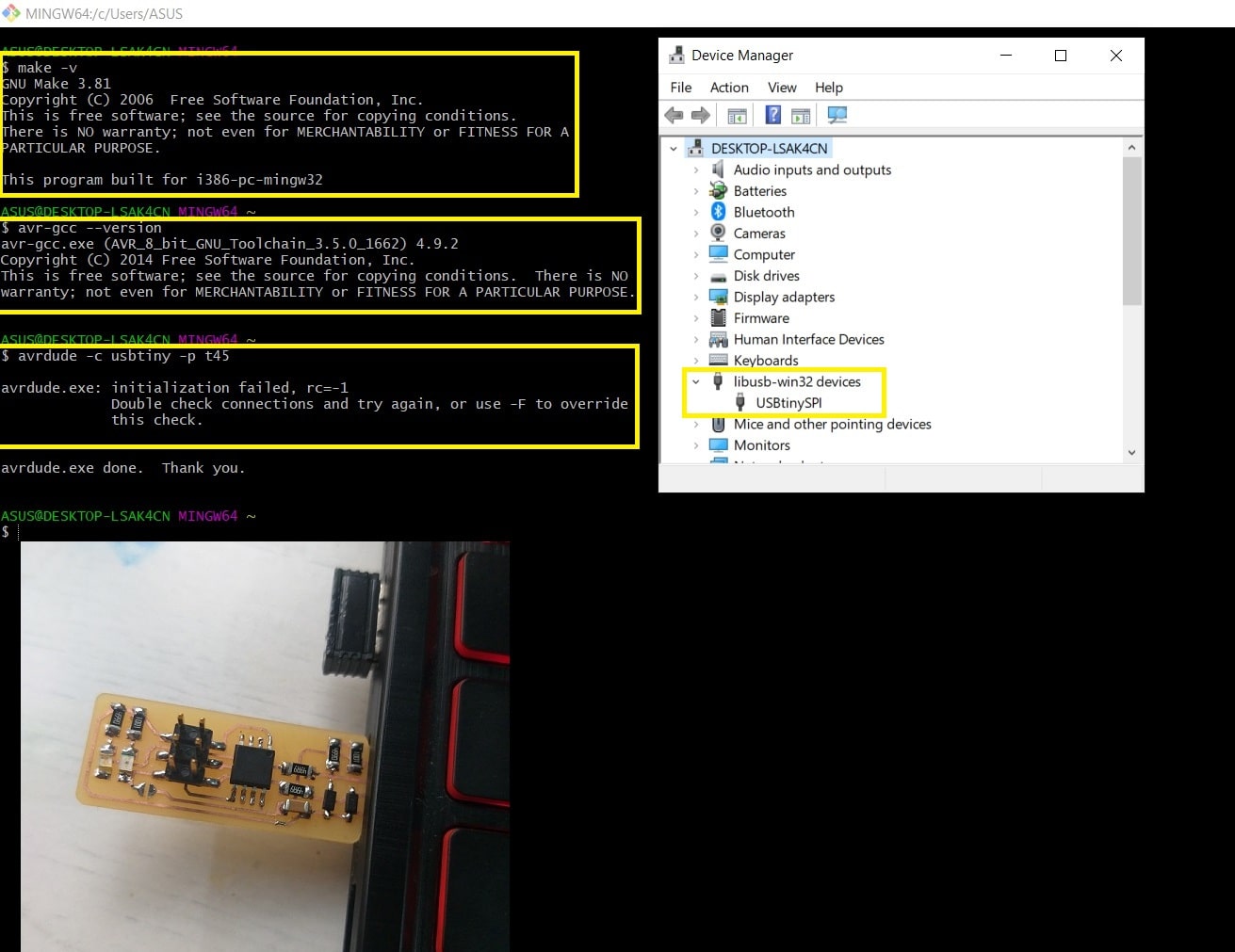
Step 6: To check your tools and drivers, start “Git Bash” and run the commands “make -v”, “avr-gcc –version” and “avrdude -c usbtiny -p t45”, if you see the same response in command then you are good. Also, check that the programmer is listed it “Device Manager”.
Programming the FabTiny ISP
To program the board I used another FabTiny ISP that was already programmed. Image to the left shows the FabTiny ISP target board, and to the right shows the programmer used.
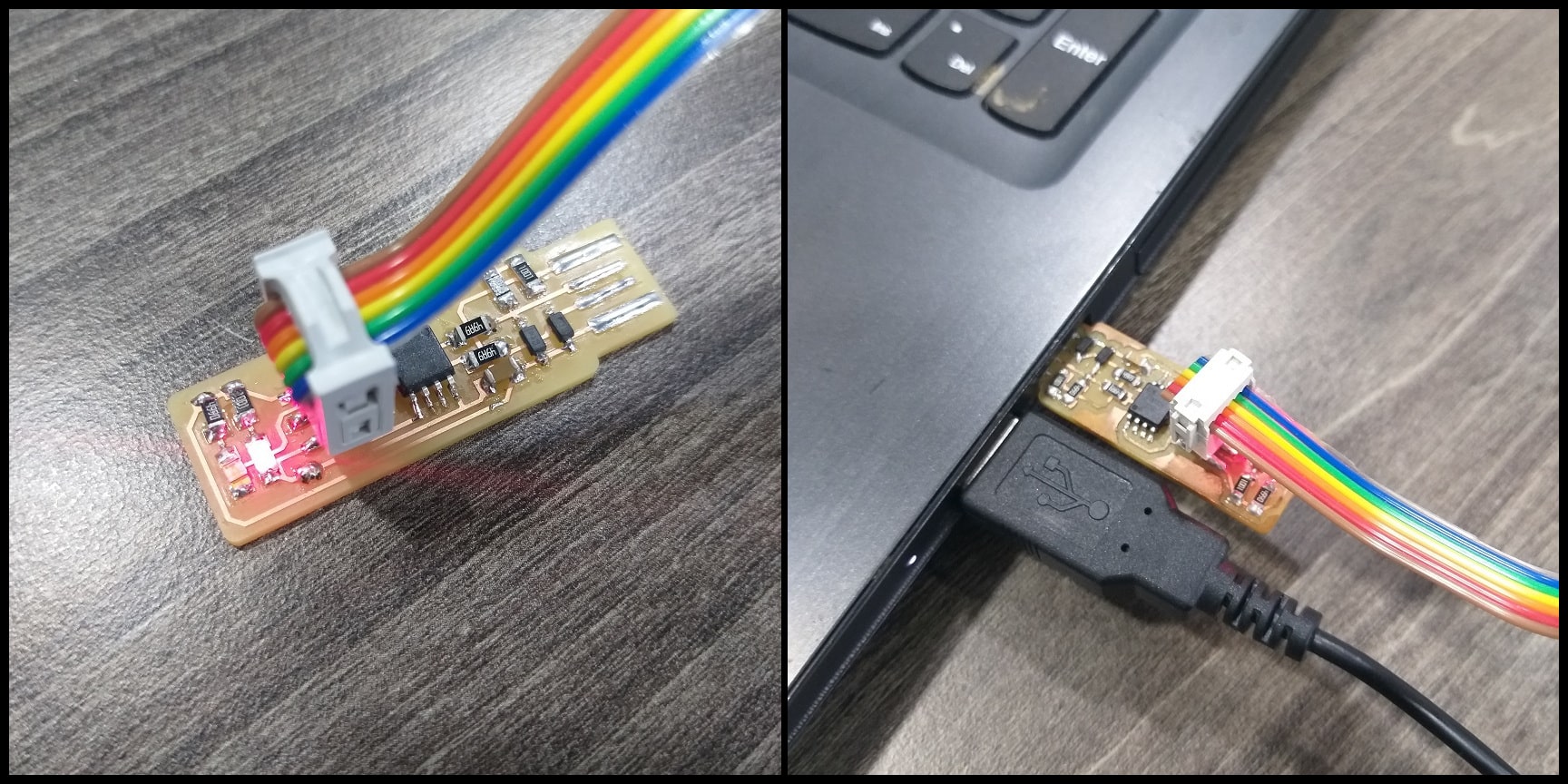
The programmer and the FabTiny ISP target board are supplied from the PC USB port. Make sure that jumpers are bridged in both to power the boards. Now we are ready to use the programmer to program the new FabTiny ISP.
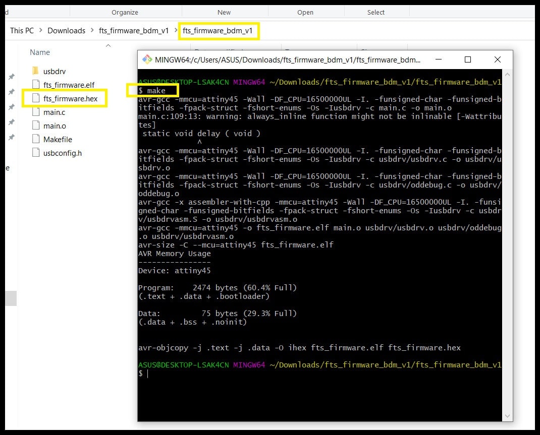
Step 1: Download “Firmware Source Code” ZIP file and extract it. Run “Git Bash” inside the folder “fts_firmware_bdm_v1”.
Step 2: In “Git Bash” command window run “make”. This will generate “fts_firmware.hex” file, which will be programmed to the target FabTiny ISP. Note that the default programmer defined in “Makefile” is the “usbtiny”. You can check that by opening the “Makefile” and look for “PROGRAMMER ?= usbtiny”. If you are using another programmer you have to change here (use Notepad++).
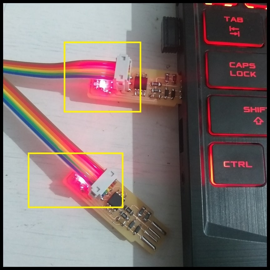
Step 3: Connect the 3x2 header of the programmer to the 3x2 header in FabTiny ISP target board. Make sure that pin 1 in the programmer is connected to pin 1 in the target board, and so on. Insert the programmer into the computer USB. Red LEDs should light in both boards.
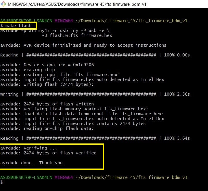
Step 4: In “Git Bash” command window run “make flash”. This command will program the flash memory in target board with the file “fts_firmware.hex”.
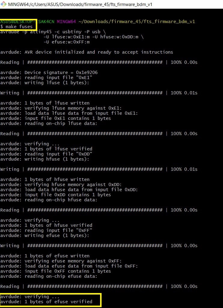
Step 5: In “Git Bash” command window run “make fuses”. This command will program some settings to make the FabTiny ISP target board a programmer.
Step 6: Disconnect the cable between both boards, unplug the programmer and insert the FabTiny ISP target board into the USB. The red LED should light and if everything is OK, you should see your board listed in Windows device manager as “USBtinySPI”.
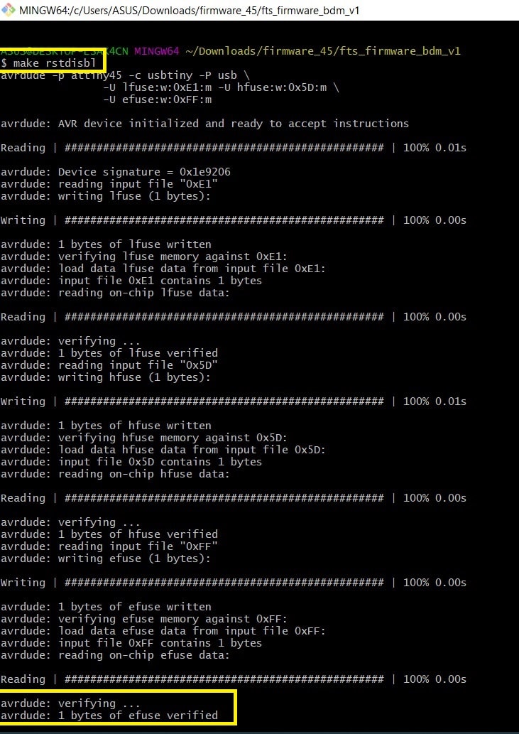
Step 7: Unplug the FabTiny ISP target board and insert the programmer to USB. Connect the 3x2 headers in both boards. In “Git Bash” command window run “make rstdisbl”. This command will disable reprogramming the FabTiny ISP in future.
Step 8: Remove the jumpers in both boards. When you use your programmer on externally powered circuits, this will prevent short circuiting between your USB and the external power supply. The jumper is necessary only when programming a circuit supplied from the USB.
Hero Shoot!