W4"Electronics Production
This document is under Construction
- in this week "The assignments", I, WE will:
- no fire
- no smake
- not dead yet.......
- Please check : Building the FabTinyISP
- also after dowiloading the sourse firmare code Building the FabTinyISP
- more explaining, you can skep this if you have the kwnolage:
Electronics
-Group assignment+-Individual assignments:
Group assignment:Group assignmentCharacterize the design rules for your PCB production process
So PCB, OK that is new for me, usally I use breadboards and ready arduino to build my projects, but this time....PCB this looks hard in the first time, espacially soidering the small parts..... lets try it: first of all, we are using Carvy milling machine, this is the first time for my yo use it for PCB, from what I read on the website and the electric parts that the lab bringed to us, we will use 2 bits for making the PCB; first one is milling head with 1/64inch size, and the other one if for cutting with 1/32inch size. one onre info the PCB depth is 1.2mm so we are cutting in respect with that depth.
extra..... from preivous expeiance; cut with steps, dont cut all the depth in one move... you may break the cutting head.
put the PCB in place and hold it in possion using the scroos in the sides ( blue color)
the machine in the lab has an aditional layer between the wood base and anything we cut (black color), so we dont cut in the wood base.....and the black layer is stabled with 2 green scrows in the sides:
how about the bits, what sizes you are using.....will the machine is setted up with 1/64inch bit for milling, and if you want to change it for cutting, then all you need is a 2 holing tools and some forse in moving the head to untite the bit and insert the new one, thne titen it agian:
here are the 2 bits that I am using, 1/64 in for milling and 1/32 inch for cuttinig:
how to make sure that the surface that you are wotking on is stable, other that the 2 scrows from the machine, will, I am using a double side time for that:
let the machine cut:
one min ..... how did you control the machine?
weeelp, we are using Easel software (online) to do that, throuth an account in Inventables, go check it on this link:Easel
simple and easy interface....just look at that smaily face!
Thank you for the ISP model, that was a fast spet to do, lets improt it:
first test was bad, second one as 2 was not the best, some lines were very thin:
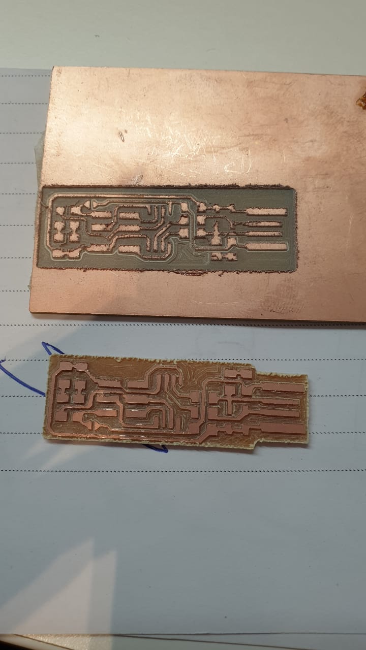
lets make more..................but this time, becarful while intering the sitting in the software, ooohhh very smart...
and what are the sittings? your really like to ask about everything, fine check this:
as you can seen, first we will mill the part, with the follwing depth of 0.1 mm and 1/64 inch bit:
More cutting, but this time with the correct sitting and the correct steps
as you acn seen, the mill is better here:
then we will cut the part with this settings:
cut depth of 1.3 mm to go throw all the pcb baord....
WALAAAA, and here we have it, a living been ISP!!!!
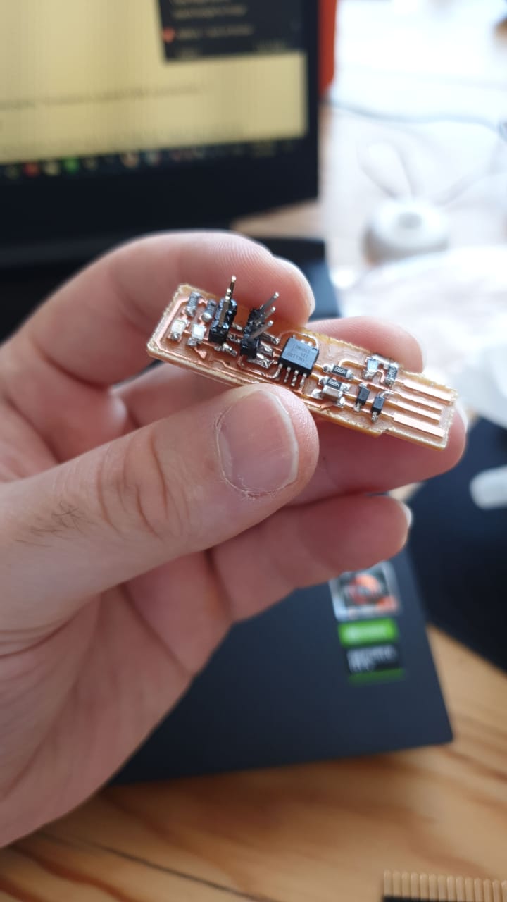
hmmm, not again....... please show by steps o_o!!
... you know that you are pain...ok here we go, whatch how I soildred the part:
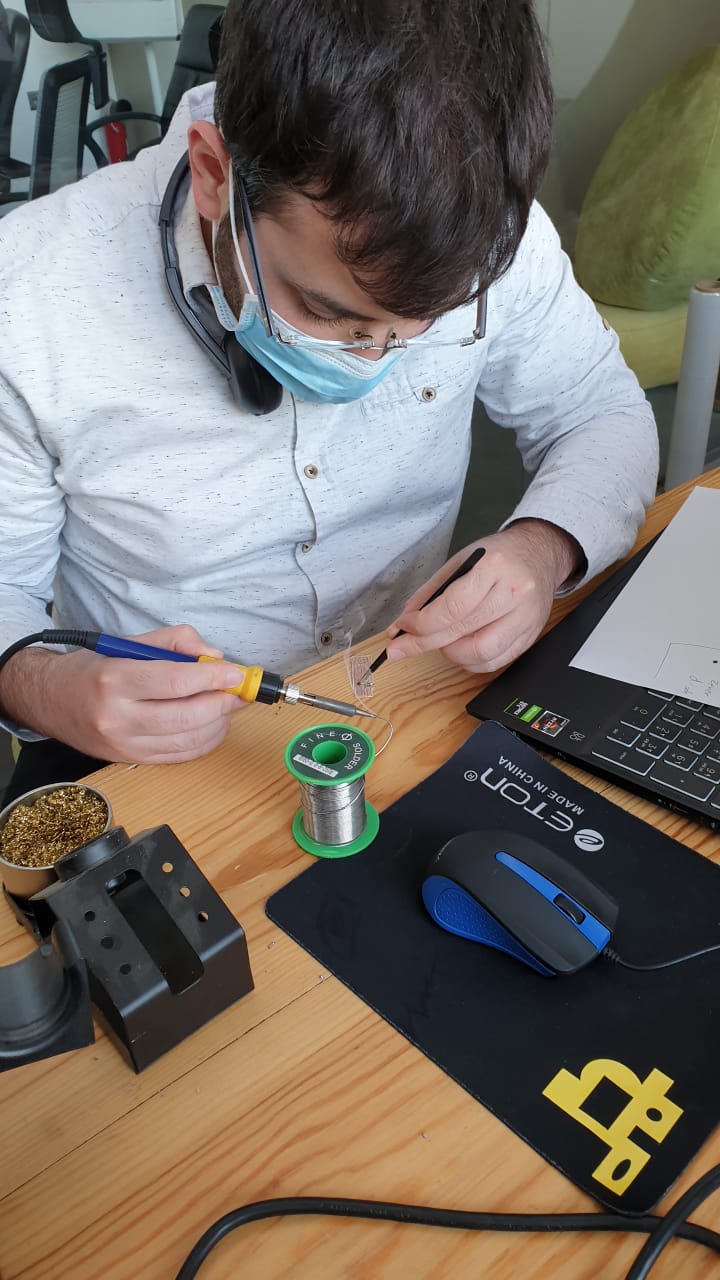
first parts:
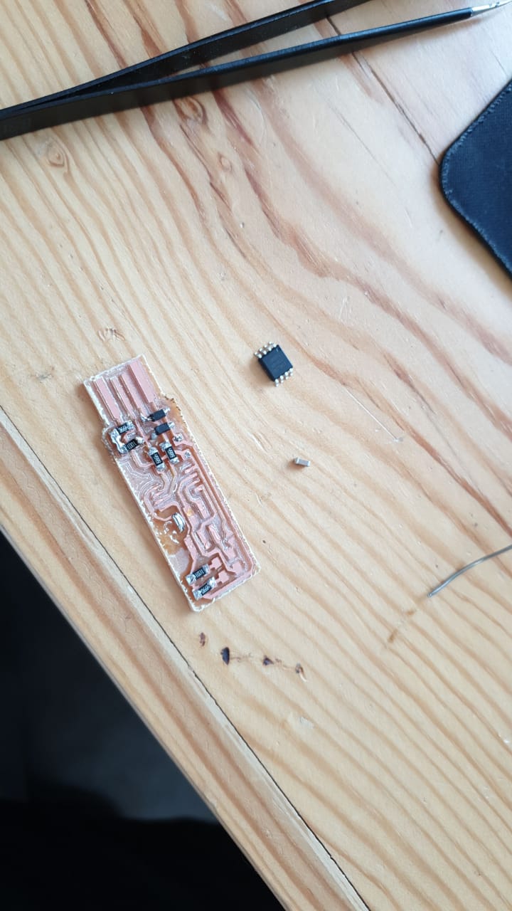
add some cabels, for testing:
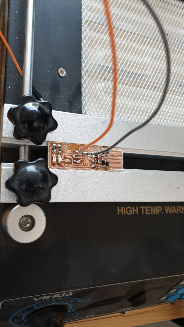
testing the connectivity of the bord using the muiltimeter:
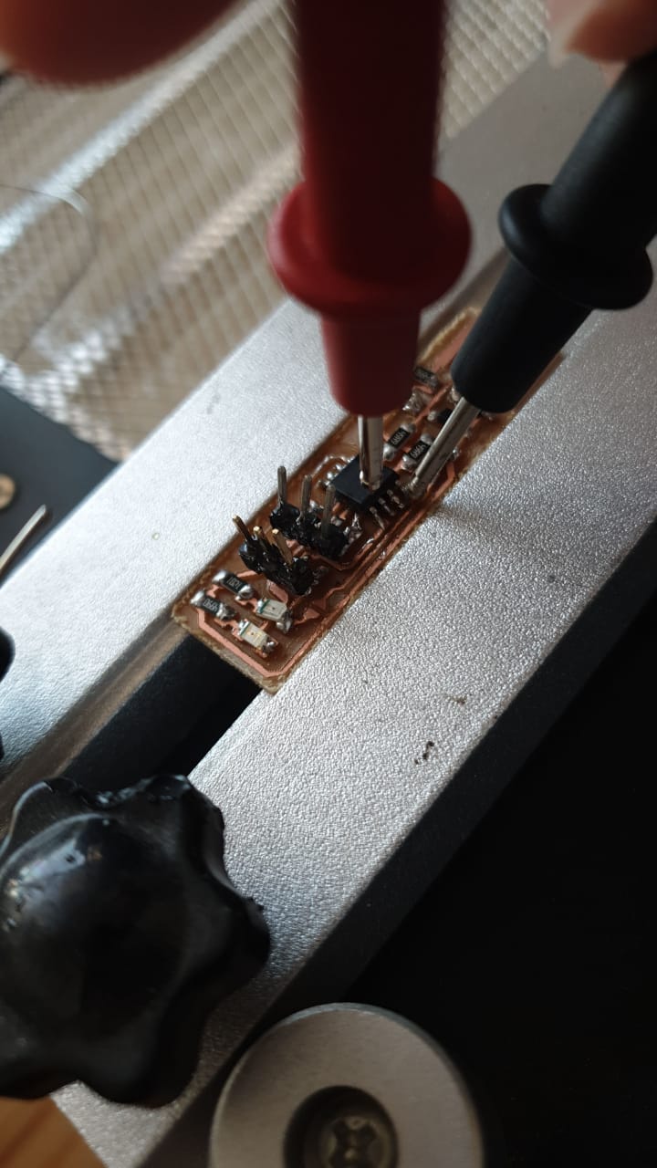
and finally agian.....WaLAAAA:

just for your info... I did the soildiring 1233411 time, and you will find the resolts below in (Some Problems WE faced)
anyway, after building the ISP, it si time to program this little cute thing:
ofcourse after testng the electric connectsions in the ISP and makesure that all connectsions are correct, I connected the ISP to my laptop:
red light on,,,,, on red FIRE......... that is a good sign right??!
how to know that you did not F up:
OK, we made it..........
now lets program it with the same steps that are mentioned in Fab academy tutorial, you can check it in the website, yes I know that you are smart enough to do that.... hmmmmmm, ust doing some MAKE CLEAN, MAKE and MAKE FUSE with other mysterious things:
lets setup the firmware and other things, we are following the same steps of the tutorials above ,start with git and type "make":
aheem, don't forget to add the setup images:
OK, OK , here:
in a simple way:
makusure you are using the same port for the firmware setup:
when conncetinm my arduino to the pc, it shows me that I am using port "COM7"
you can check it from computer manager, device manager, ports:
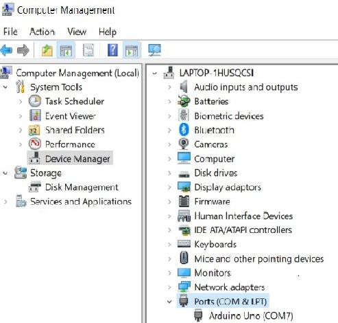
foucuse on the port com in the preaivous pic, just to make usere that your work is correct :
now, lets open GIT BUSH here, on the same file we downlaodede the firmware:
type make flash:
then type make clean:
important note: to change the port in the firmware file according to the real port that appears when Arduino is connected to, so your work will be done correctly without any erros. You can find make file inside firmware folder, edit Make file --> Edit with Atom or Note++ or any program you are suing for coding --> replace COM7 to COM3 or any port COM your aduino is using for conncetion:
doing this ("make clean" to delet old files form within the soursed firmware):and wallllllaaaaaaaaa.....we have it, blogged , runing and no one is dead!:
Still alive.........
what just happend, pal
now, let's play with the attiny85 for some fun, this should be a micro computer, so let's use the yelow led in the pcb to blink it. just to know that this is the attiny 85 pinput:
so the yellow led is conncted to pin 2 for coding , so let's blink it for 3 times then give it some break then blink again:
take a look:
OK for connceting the arduino with attiny, I am suing this concnetion:
so this 6 pins are the same as this in the eagle file from week6:
So MISO FROM PCB TO PIN 12 ARDUINO,SCK FROM PCB TO PIN 13 ARDUINO,RESET FROM PCB TO PIN 10 ARDUINO,vcc FROM PCB TO vcc ARDUINO,GND FROM PCB TO GND ARDUINO,MOSI FROM PCB TO PIN 11 ARDUINO.
you need to add this library to IDE arduino to bea ble at program any attiny85 for the future(https://raw.githubusercontent.com/damellis/attiny/ide-1.6.x-boards-manager/package_damellis_attiny_index.json)
just copy it to preferance window inside IDE arduino and copy it inside "additinal boards maneger urls", theb from tools, boards, boaords manager, search for attiny85 and instul it, check this link to understand more link