WEEK 6 - Electronics Design


INTRODUCTION

The best part about electronics assignments is that I started to like soldering :) and that was a challenge for me especially with SMD components.

Assignment Description

    group assignment:

  • use the test equipment in your lab to observe the operatio of a microcontroller circuit board
  • individual assignment:

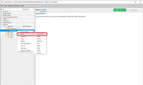
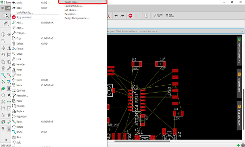
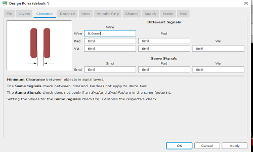
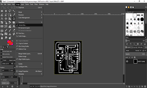
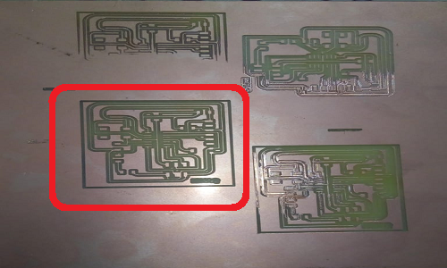
  • redraw an echo hello-world board, add (at least) a button and LED (with current-limiting resistor) check the design rules, make it, and test it

Tools and components


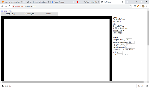
  • 1 x FR1 (Copper PCB Board)
  • 1 x 1/64 inch end mill bit
  • 1 x V bit 30'/.2
  • 1 x double tape
  • 1 x Soldering Station.
  • soldering wire
  • AVO multimeter
  • flux
  • Magnifying Glass
  • Electronic Components:
    • 1 x ATiny44 microcontroller.
    • 1 x Push Button.
    • 1 x crystal 20.000 mhz.
    • pin header.
    • 1 x 1 uF Capacitor.
    • 2 x 10k Resistor
    • 1 x 499 Resistor.
    • 1 x potentiometer.

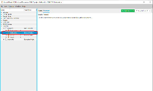
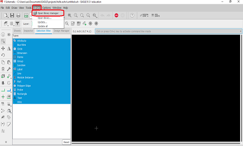
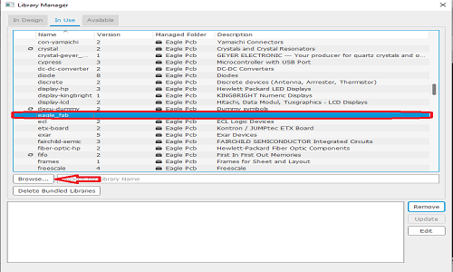
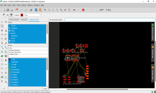
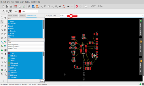
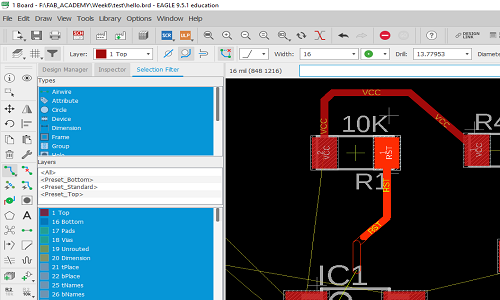
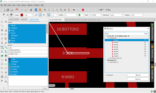
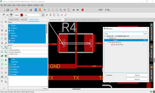
Circuit design steps


Well, before we get started, I don't have much experience in electronics design before, so let's start together.

  • At first I used Eagle software, you can download it from here
  • install and open it
  • make a new project "hello.echo"
  • Right click and choose New schematic
  • Here are some commands you need:
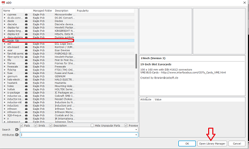
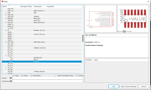
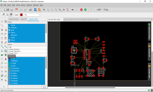
    1. Add: to add new component
    2. Move: for moving and rotating
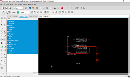
    3. Net: to connect the components together
    4. Name: Each point must be named to connect them easily
    5. value: for componentes values like "10K, 1uf"
  • before we start you need to add FAB_lib, you can get it from here
  • You need to put your file in a similar directory "C:\Users\zas\Documents\EAGLE\libraries"
  • Then go to library manager, and open "In Use tap"
  • then click on Browse, and choose your file(Eagle_fab)
  • now your library should be appear when you type Add command, If it does not appear with you, you can check the library manager
  • Now type "Add" command and choose UC_ATTINY44
  • left click on the workspace to put your component, and right click if you need to rotate it
  • press on Esc to return to the library again
  • Add the rest of the components with the same previous steps
  • type "Name" command and name each point
  • type "Net" command and connect the same points that bear the same names
  • click on SCH/BRD to go to the Board page
  • You need to try to put each component in the correct position, you can follow the current to do so.
  • Then you should go to the design rules to set the dimensions for your path, Unfortunately I forgot this step here!
  • Type the command "route"
  • Then start connecting the path between the components
  • After you're done, go to the design rules again, to check the dimensions of your path.
  • If you forgot to set your dimensions from the start like me, you'll almost find errors.
  • So,I followed every error to correct it, you can say I redesigned again
  • After that, go to layer settings, and hide all except Top and Bottom
  • Then, choose file>>Export>>Image
  • check the monochrome box
  • put the resolution 500 dpi
  • I used Gimp, you can Download it from here
  • and I follow this Tutorial
  • just convert the traces to white, and the rest of image to black.
  • and make boarder around the image
  • finally, go to the fab modules like Electronics Production week
  • Miling and Soldring
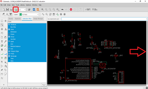
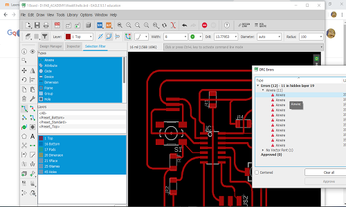
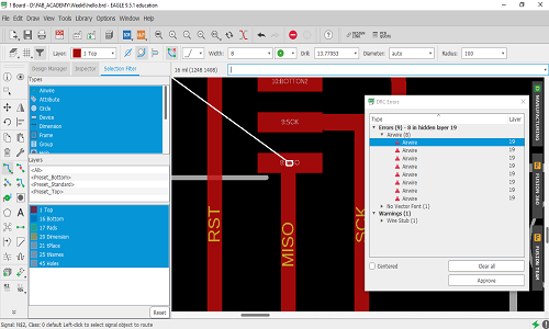
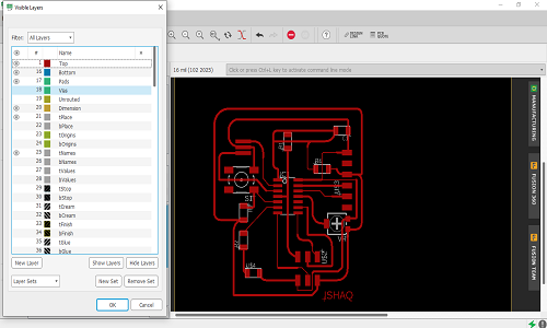
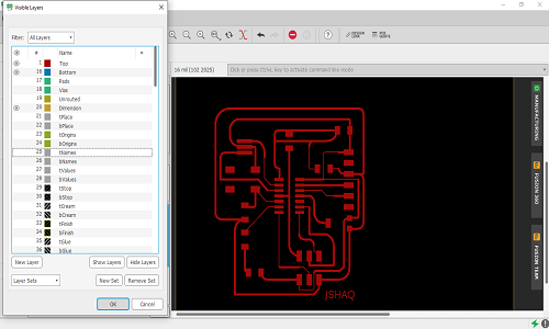
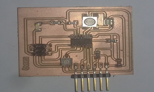
  • And here I tested it :)

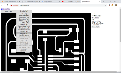
    Download all files from here