6. Electronics Design
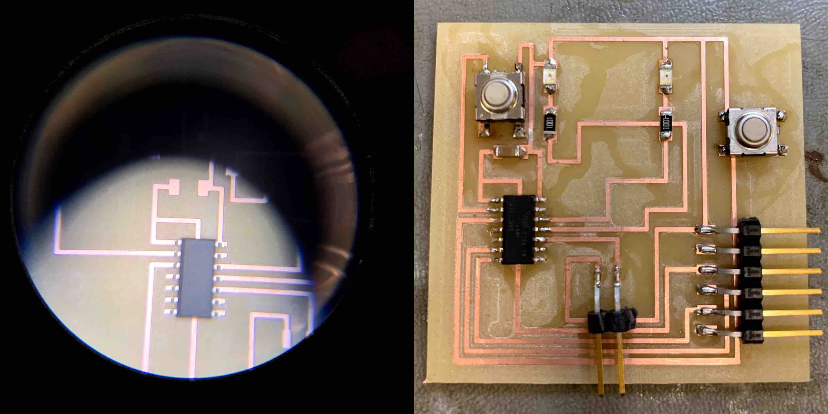
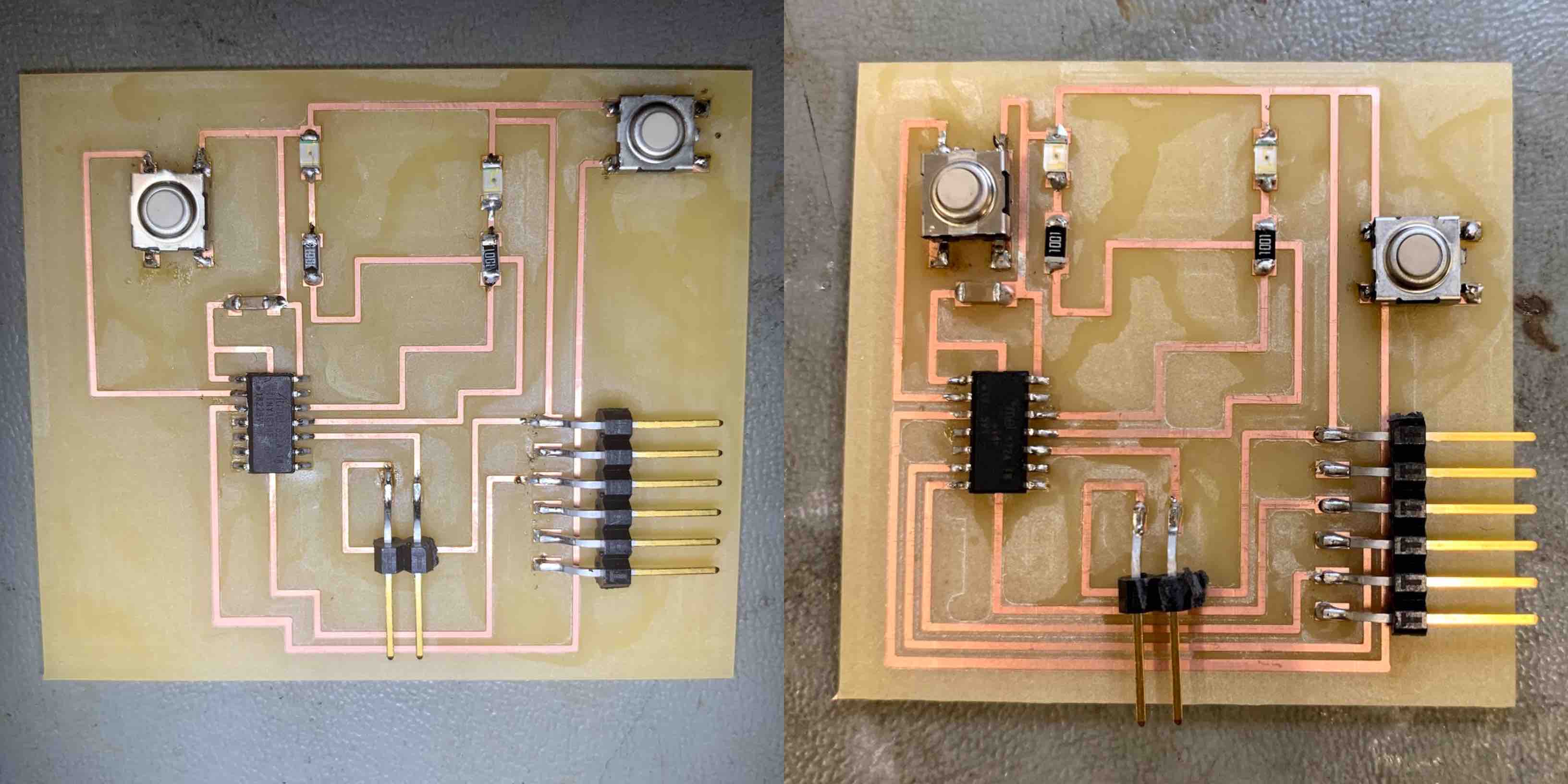
This week I worked on designing, cutting, soldering and checking my creation of the AT Tiny 1614 hello board with 2 LEDs and 2 push buttons added.
Research
In order to complete this assignment I had to download a program called Eagle (the link can be found bellow). This program allows you to import libraries and footprints of parts needed. With these pieces it helps to layout the board and the circuit routs. I completed this and used the file to cut my board. I then soldered my necessary components to my board and tested it for connection.
Useful links
Eagle
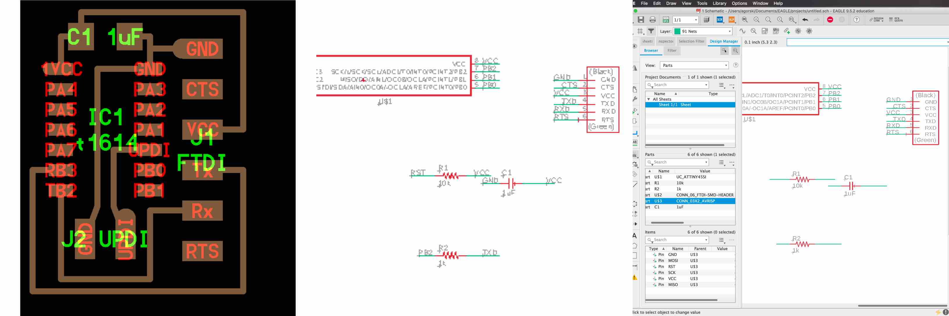
Eagle is a software created by Auto Desk. It is linked to the download and use of Fusion 360. Both programs I have found support the design functions necessary to manufacture goods. Eagle allows you to build a schematic that shows what components are being used, adjust your routs and see the layout before cutting the board. When initially using the program I found that the components I needed were not in my library or the FAB library I imported. To get familiar with the program I decided to start by constructing the ATTiny45. These components I had already seen in my inventory. When I was satisfied with my comfort level using the Eagle Software I then completed the same steps to create the ATTiny1614 that was for the assignment.
Each of the hello boards were provided on the assignment page. This allowed the user to view the basic layout expected. This I also found helpful to double check your connections. With the addition of the LEDs and push buttons there are some difference, however the routs necessary to connect all other components are shown.
To use Eagle you must first open a new project. When in the New Project the next step is to create a new schematic. This opens a new window that allows you to use the loaded library to pull in specific components.
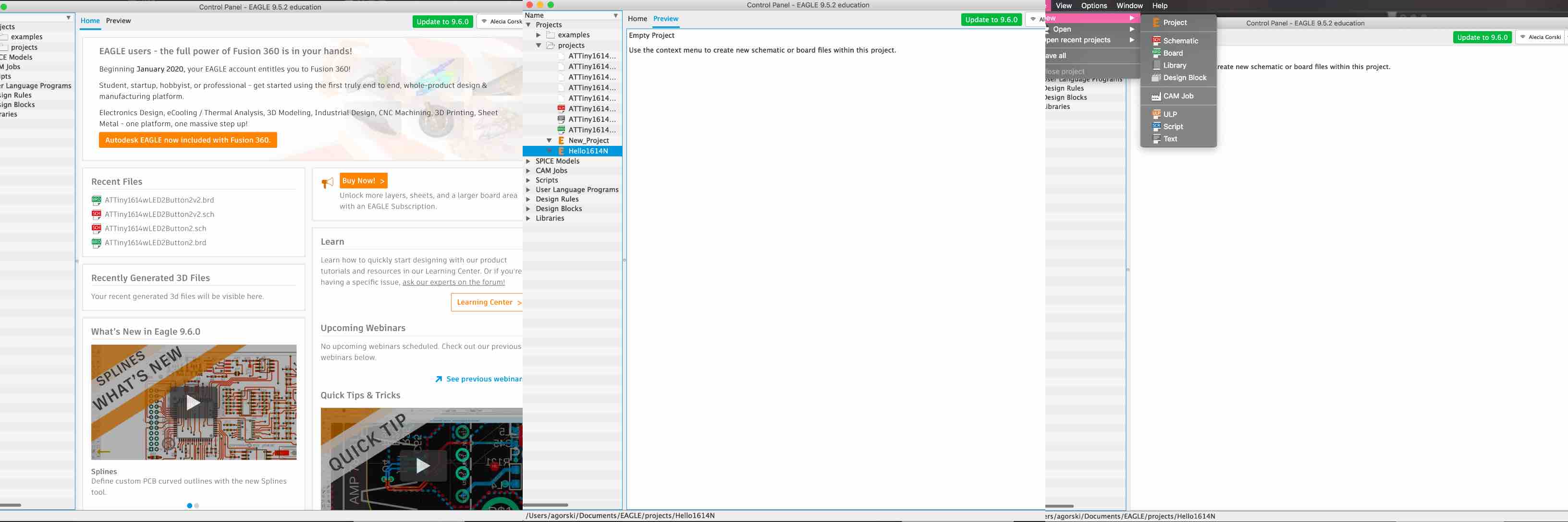
With the new schematic window open there will be a tool bar along the left side of the screen. This will provide the user with the many different options it may take to design your board. Halfway down the tool bar there is an option that looks like the plug end of an outlet. This is what you select to begin flowing in the many different components needed.
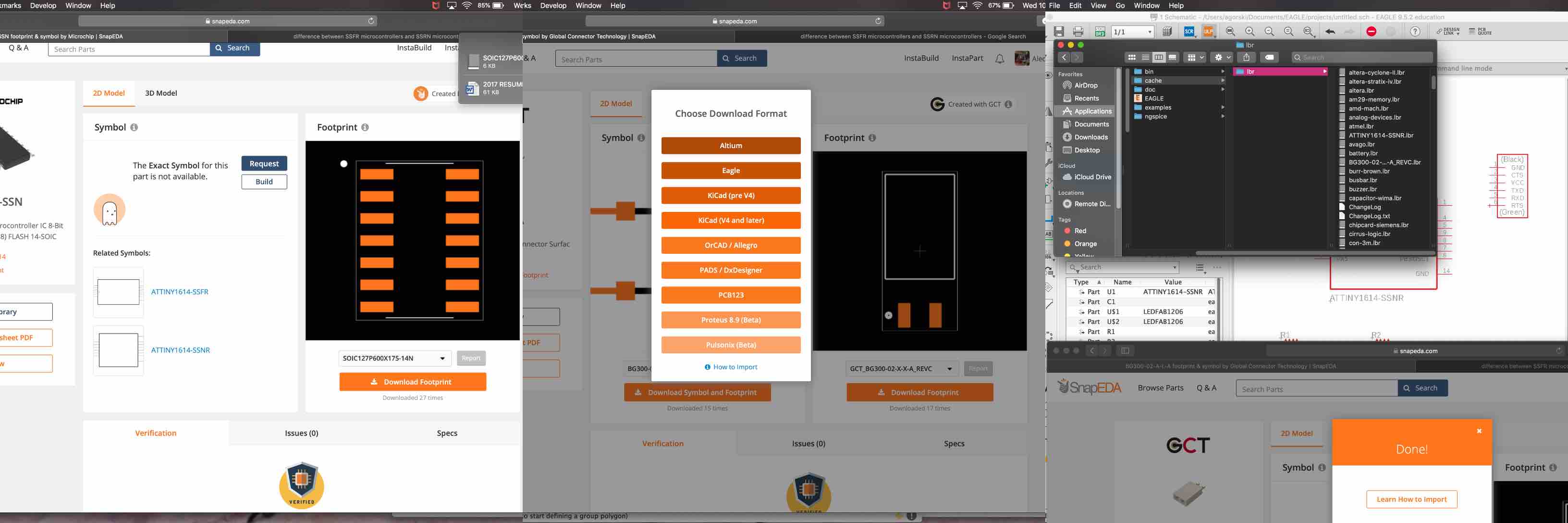
As mentioned above I originally could not locate the components I needed to recreate my ATTiny 1614. In order to obtain these pieces I was able to use an online resource called SnapEDA. This site allows you to look up any part they provide for sale. As an addition to this they allow you to download a symbol and a footprint for each piece. The symbol and footprint are provided for many different software options. This can be imported for the Eagle Library to use.
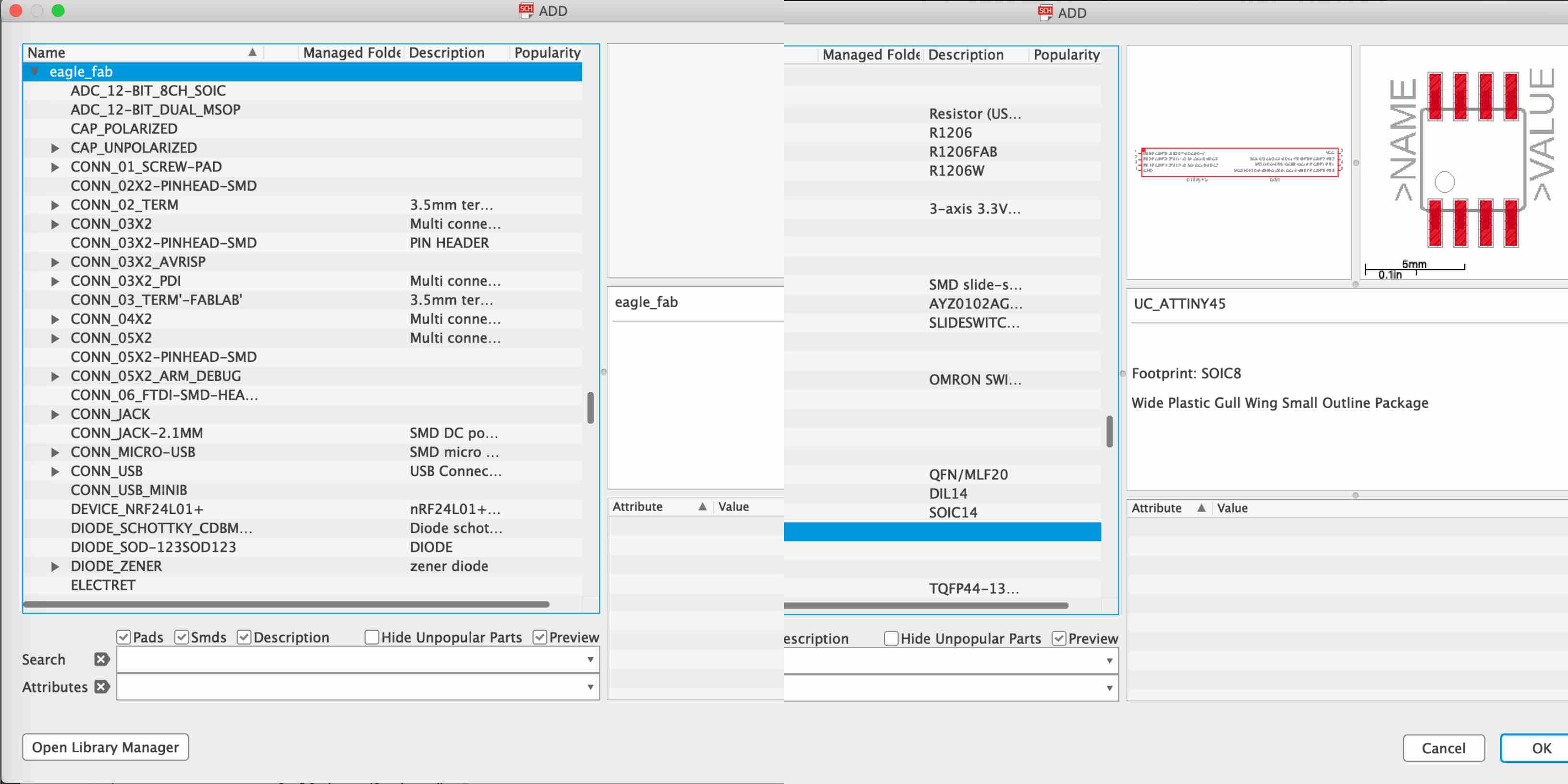
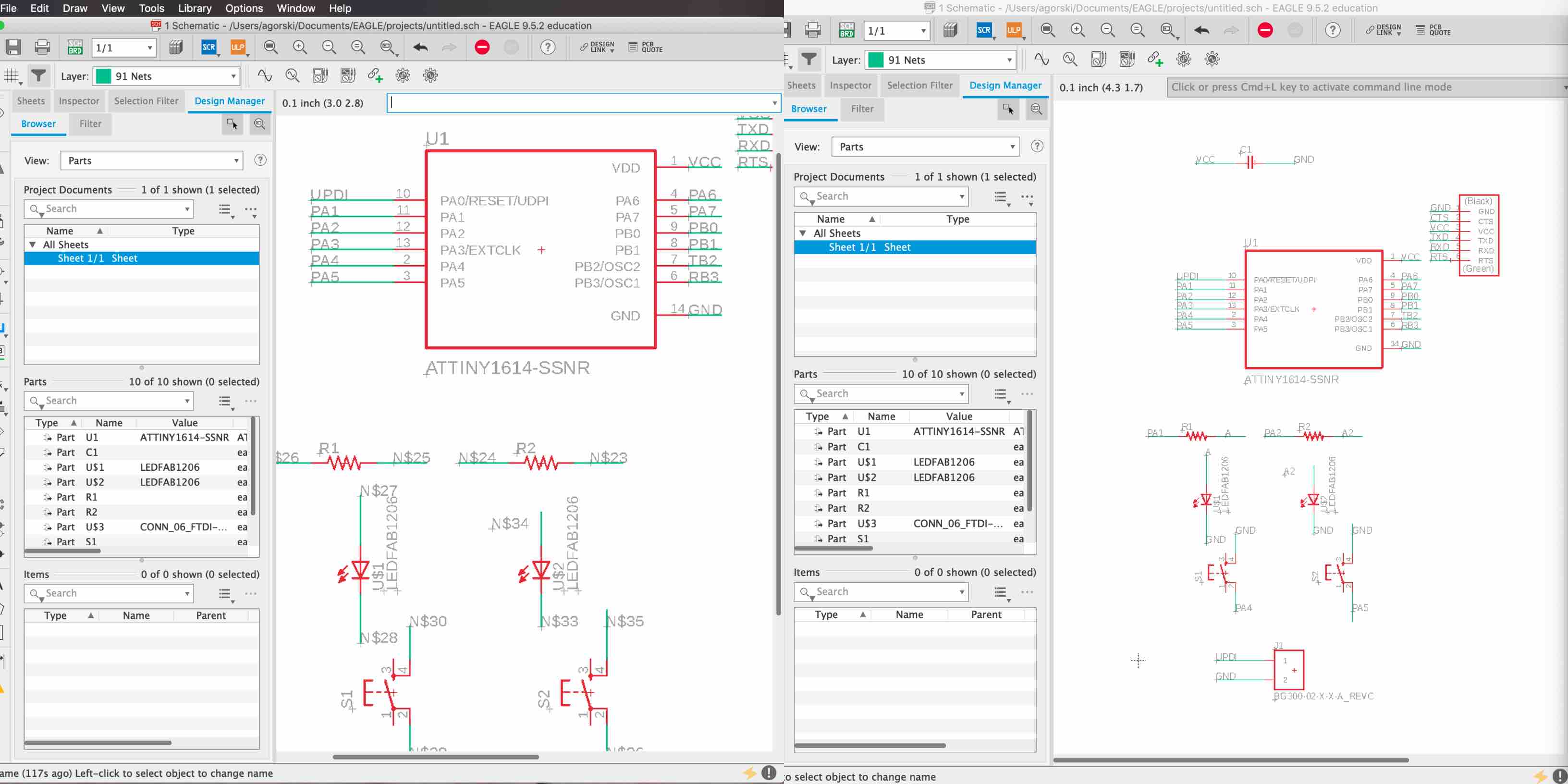
Once your library is updated for all the necessary parts it is time to begin adding them all to the schematic. By selecting the “add part” thumbnail that shows as a plug in and a green plus mark, the user now is accessing a new window that represents the library options. After navigating through the library to find the component needed select the okay button. This now redirects you back to your schematic. The schematic may be blank if it is the first component you are placing, or it could have an array of previously added components. PLace the component in the corresponding place, this can be based off of you prototype drawling or educationally guess the placement.
When all components have been placed in their intended location you can now begin adding wires to the components. The wire option is located on the left hand tool bar and shows a thumbnail of a line that id green and has a right angle at the end. The wire representation only needs to extend from the components where they connect to the circuit. For example, when placing LEDs there must be one side connected to the ground and the other connected to a resistor to control energy flow. In this case you would draw a green wire extending from each side. The wire then ends shortly after the first creation point. This wire should extend from all components.
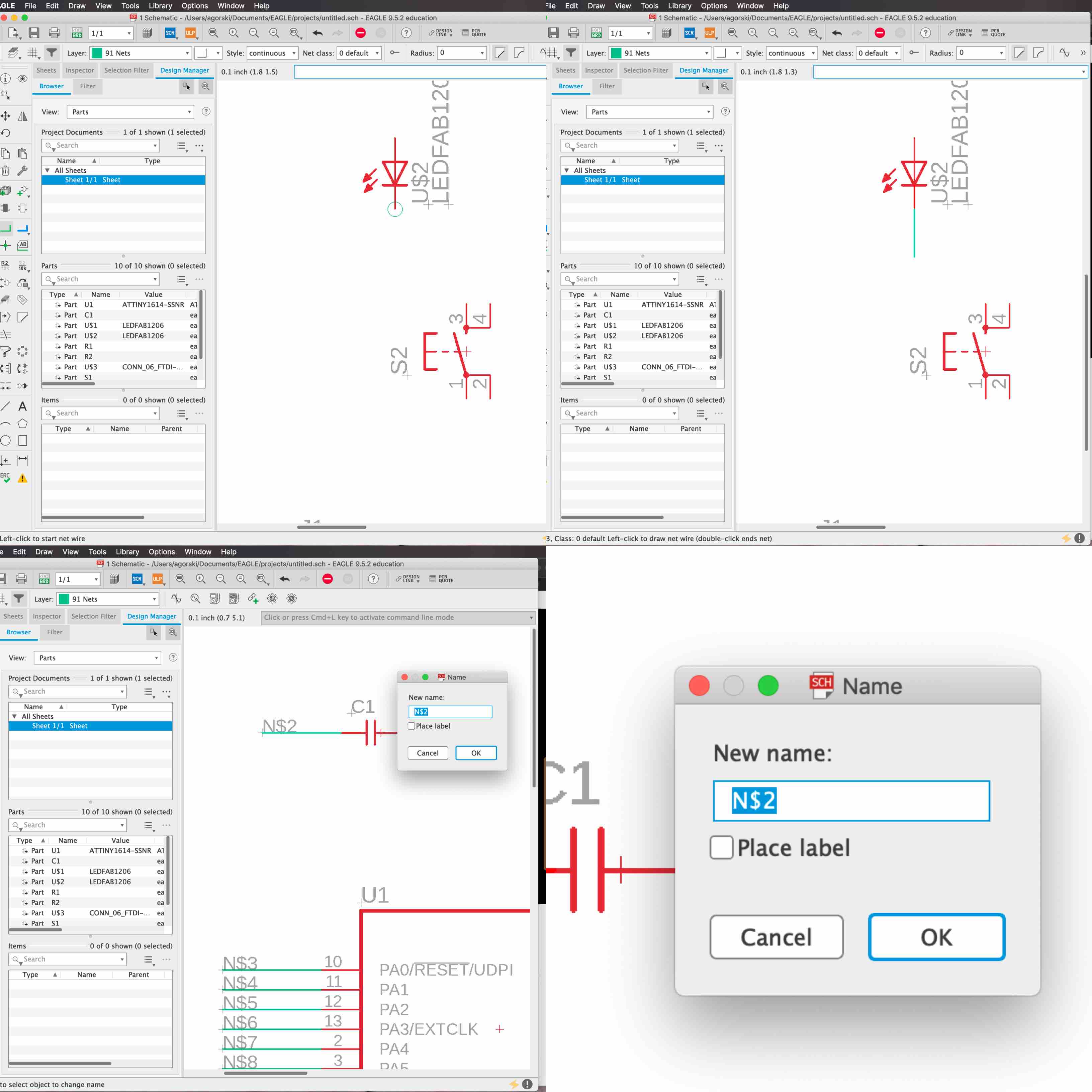
Once all components are equipped with the wires they can now be labeled. This is very important. The thumbnail is represented by a cursor with an abc label. As you label each wire you are assigning it a certain Title. This Title then assigns it to that role. The role it plays is important. For example, every wire now labeled with GND will take the roll of Ground. These will then all ask if you would like to connect them. By selecting yes each of these will connect with an invisible line that is yet to be seen. This is important to keep the flow of current assigned in the correct place.
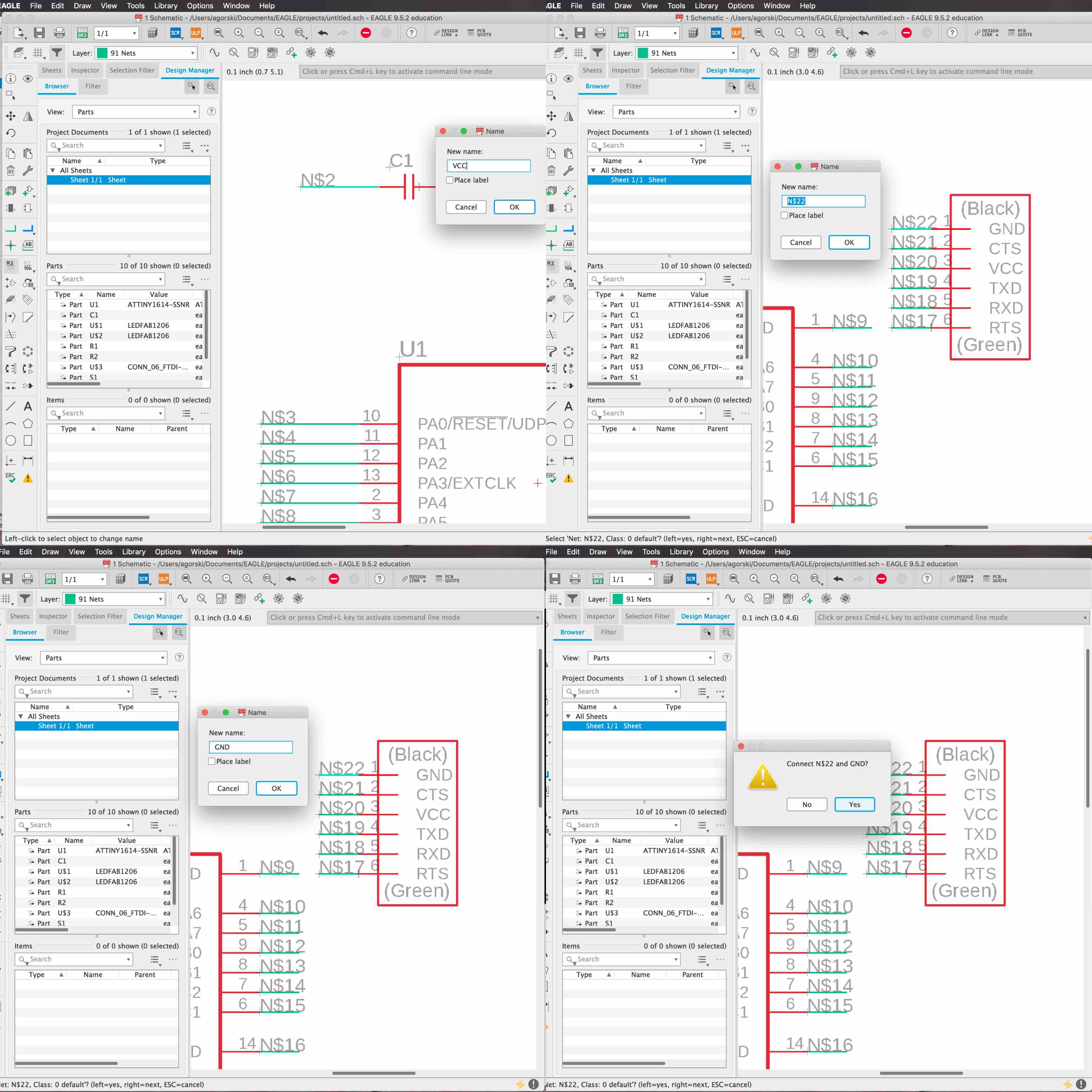
Once each extension of every component is wired and labeled within your schematic you are ready to move on to the next step in the board design process. The schematic allows you to place components and connect them through simple labels. This allows an easier way to rout your components while reducing confusion. Once your schematic is complete the user moves on to the board layout.
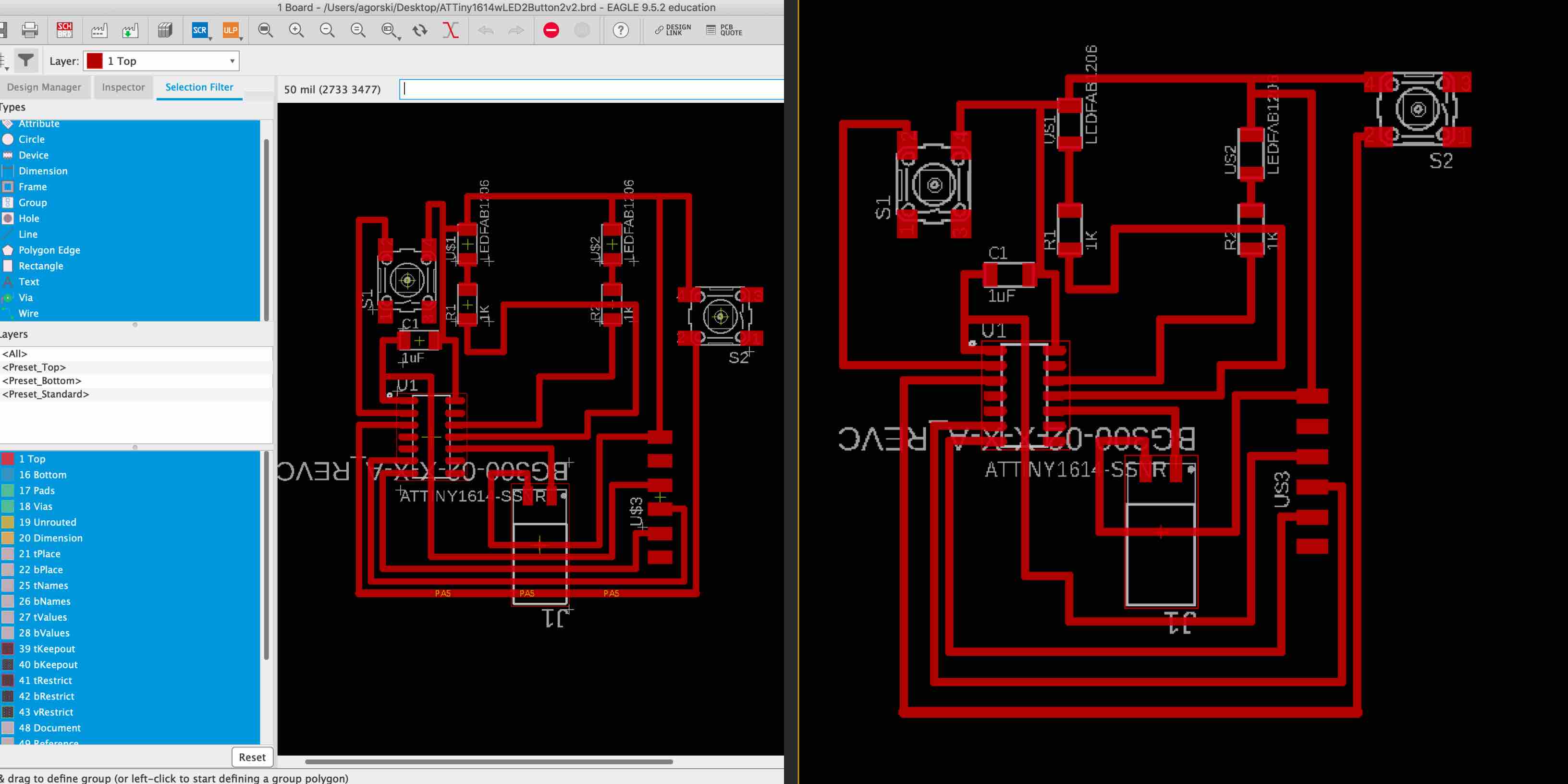
The board layout will now provide you with the connections between each component. At first this can appear very confusion. It will be like a puzzle to untangle. There are a few design rules that should be considered in the process. There can be routs that run under other component bodies, be sure however that there is enough room under the size of this component that it does not interfere with the overall circuit. As an example, there can be a rout under, from the top to bottom, the ATTiny1614, however there can not be one from side to side where the pins are located. There is not enough room between pins to then rout a path connecting other components. Another good rule of thumb is that non of the rout or paths from component to component intersect. There should never be crossed paths. This is because the entire board is made from the same layer of copper. If there are intersection routs this could confuse the current and allow it to travel in the wrong direction. This, as a result, could blow the circuit and effect many of the components when attached to a power supply.
The tool bar on the far left side of the board construction view allows the user to move, rotate, and create the routs based on the unscrambled layout.
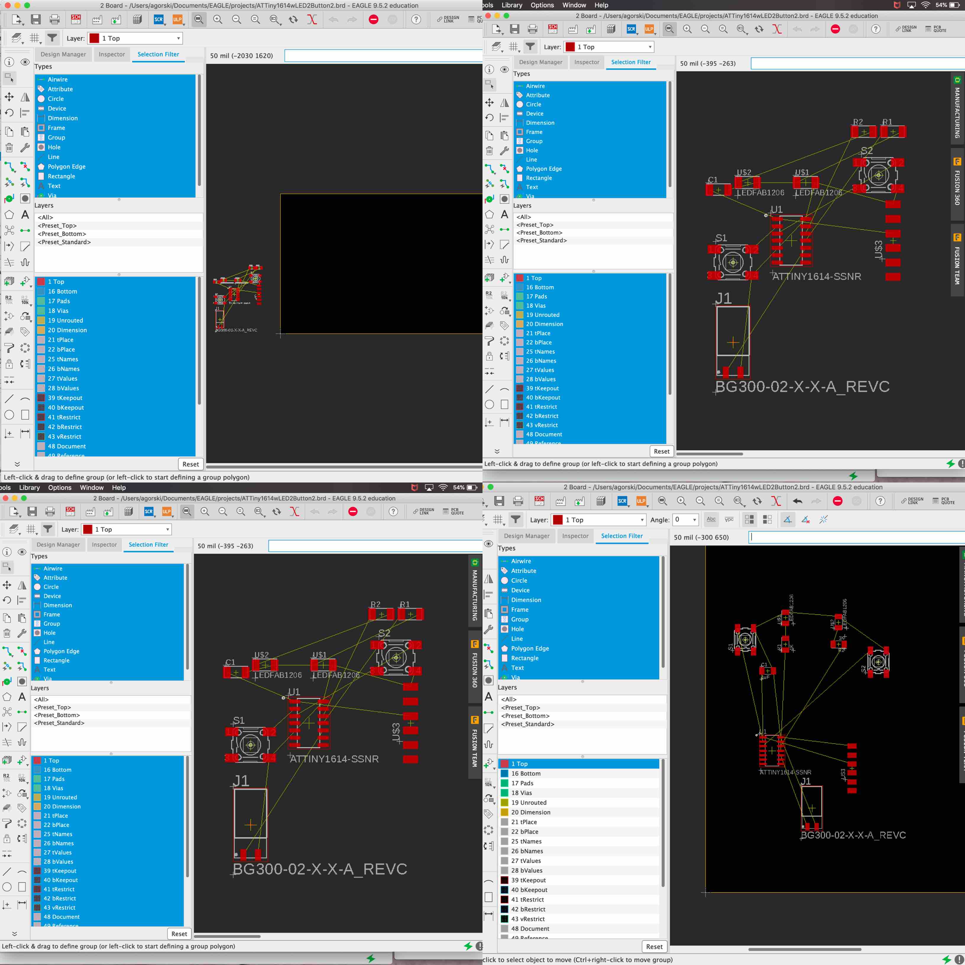
Once the layout of your board is unscrambled and each component is placed into a proper place there can now be official routs created. The routs are made with the tool on the tool bar on the far left that is represented by two dots connected by a green line. This is t;o show the final representation of the connection. When connect between components the line will become a solid red rout set to the alloted thickness. To be sure that it is correct you must change this value using the tool bar along the top of the screen. It defaulted, in my project, to being 6 mm however I needed 24 mm. I then selected my routs and adjusted them to the correct value.
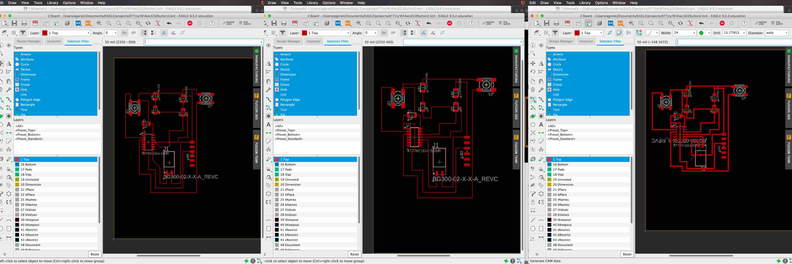
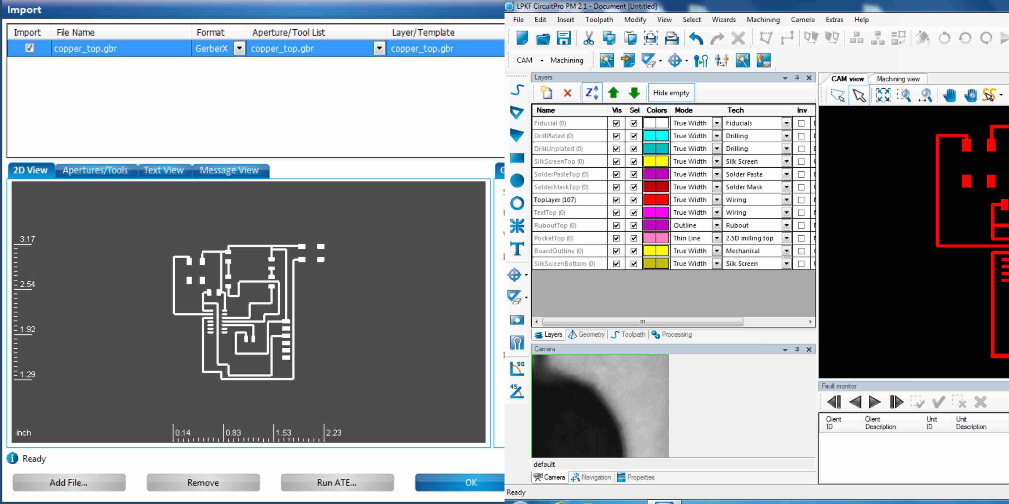
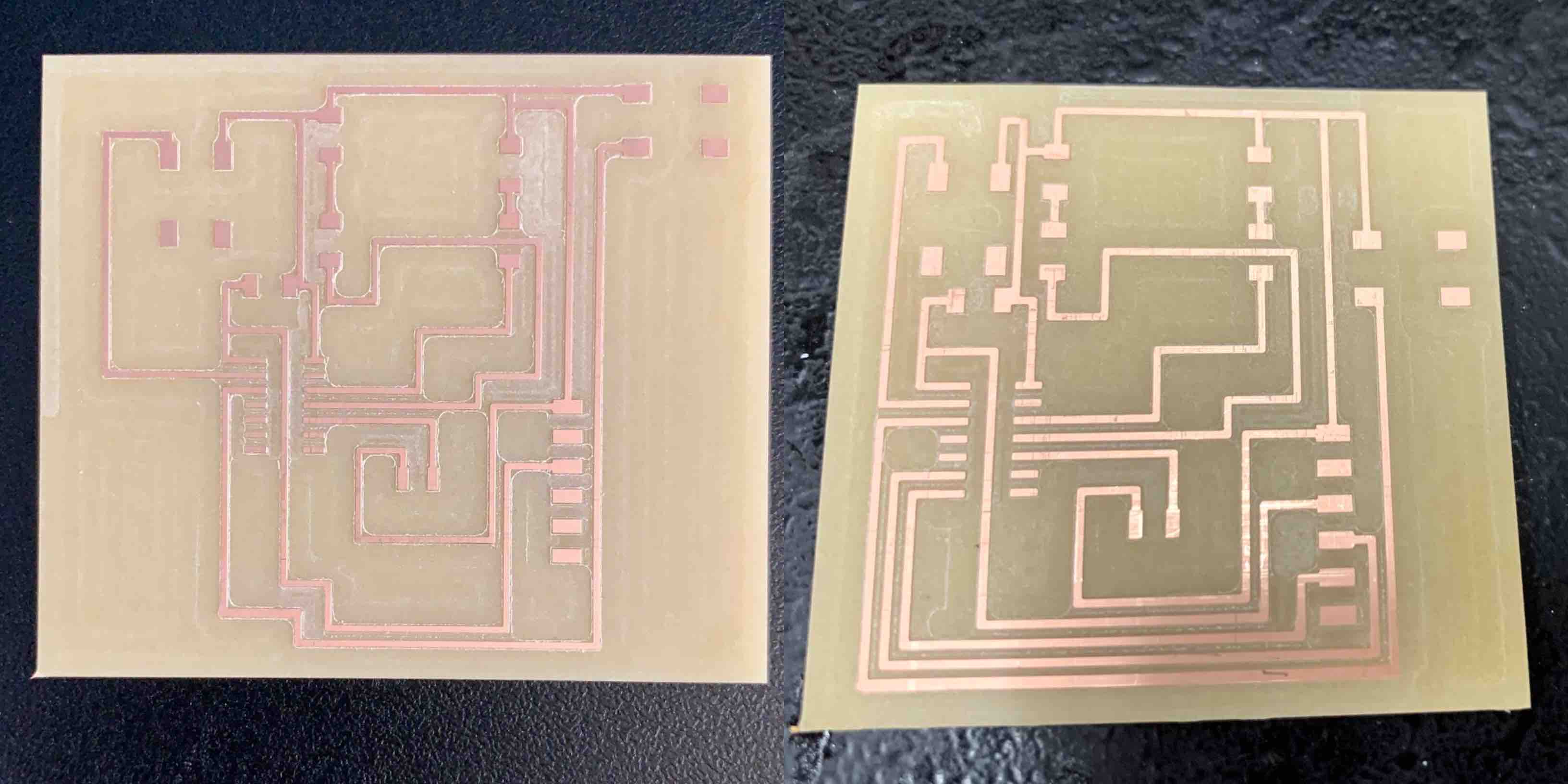
When the component are in the correct location, all routs are represented from active pin to pin and with no intersections your board is ready to be cut. However, in order to cut your chip you must have a file that communicates the correct format. For the LPKF that we use in the LCCC lab we needed a Gerber file. This is the file type that interacts with our machine. TO do this I exported my file and chose it to save as a Gerber File. The board designed below was the final design I decided to create.
LPKF
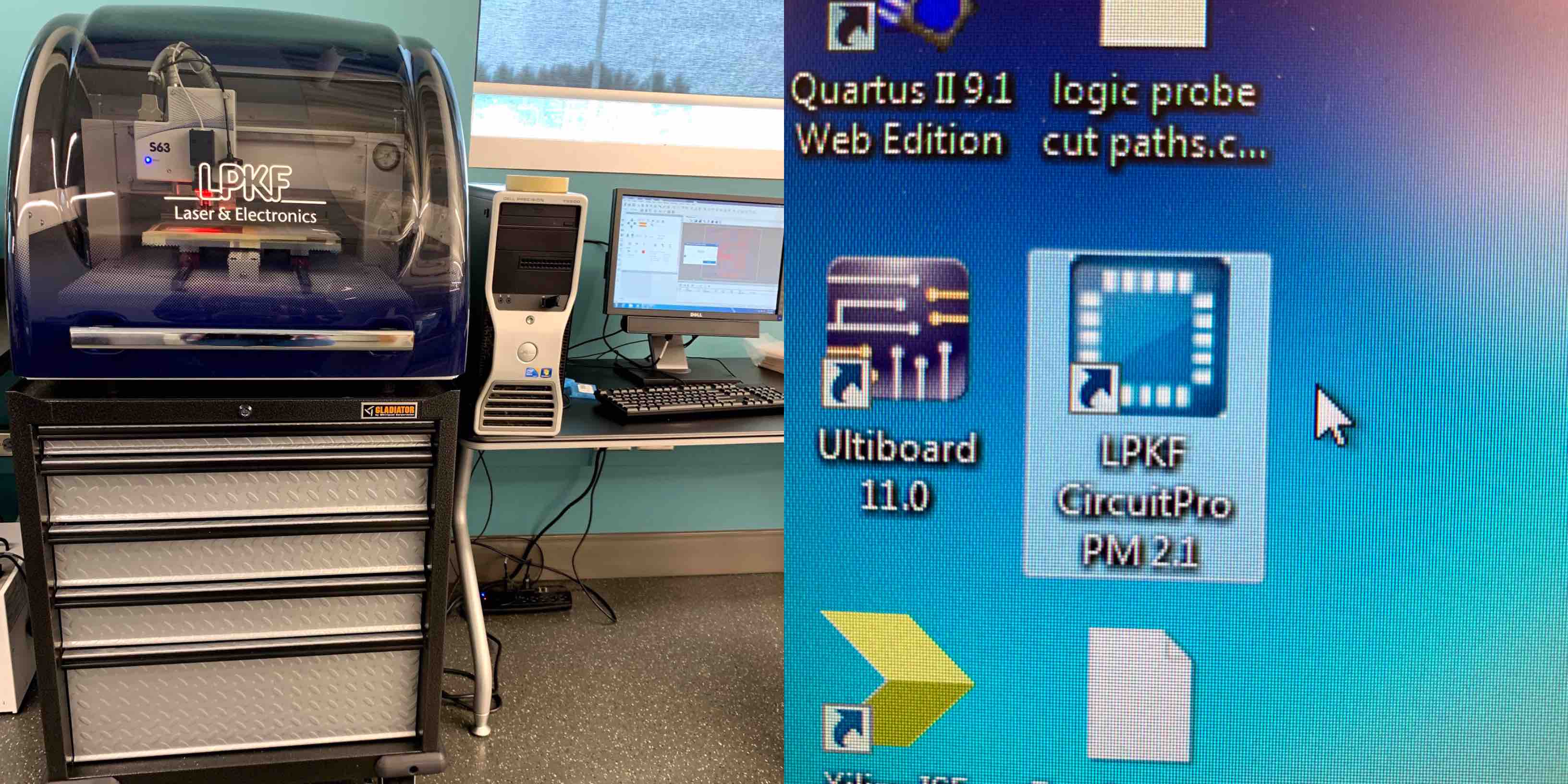
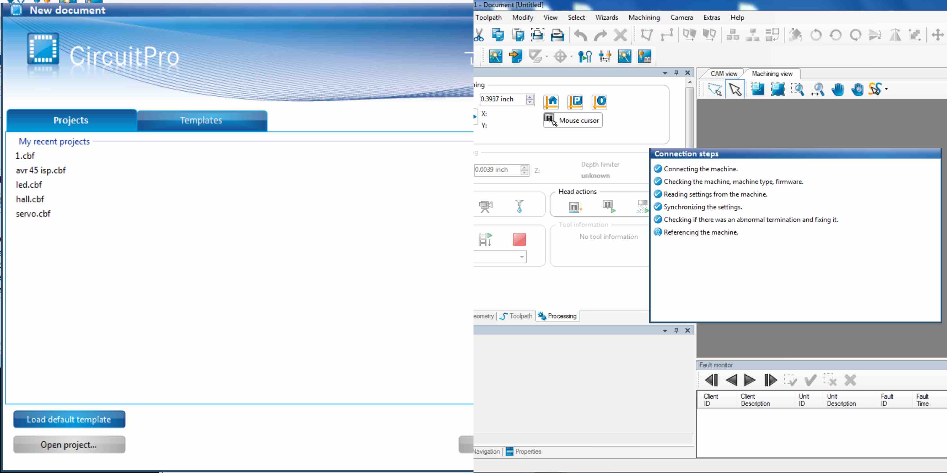
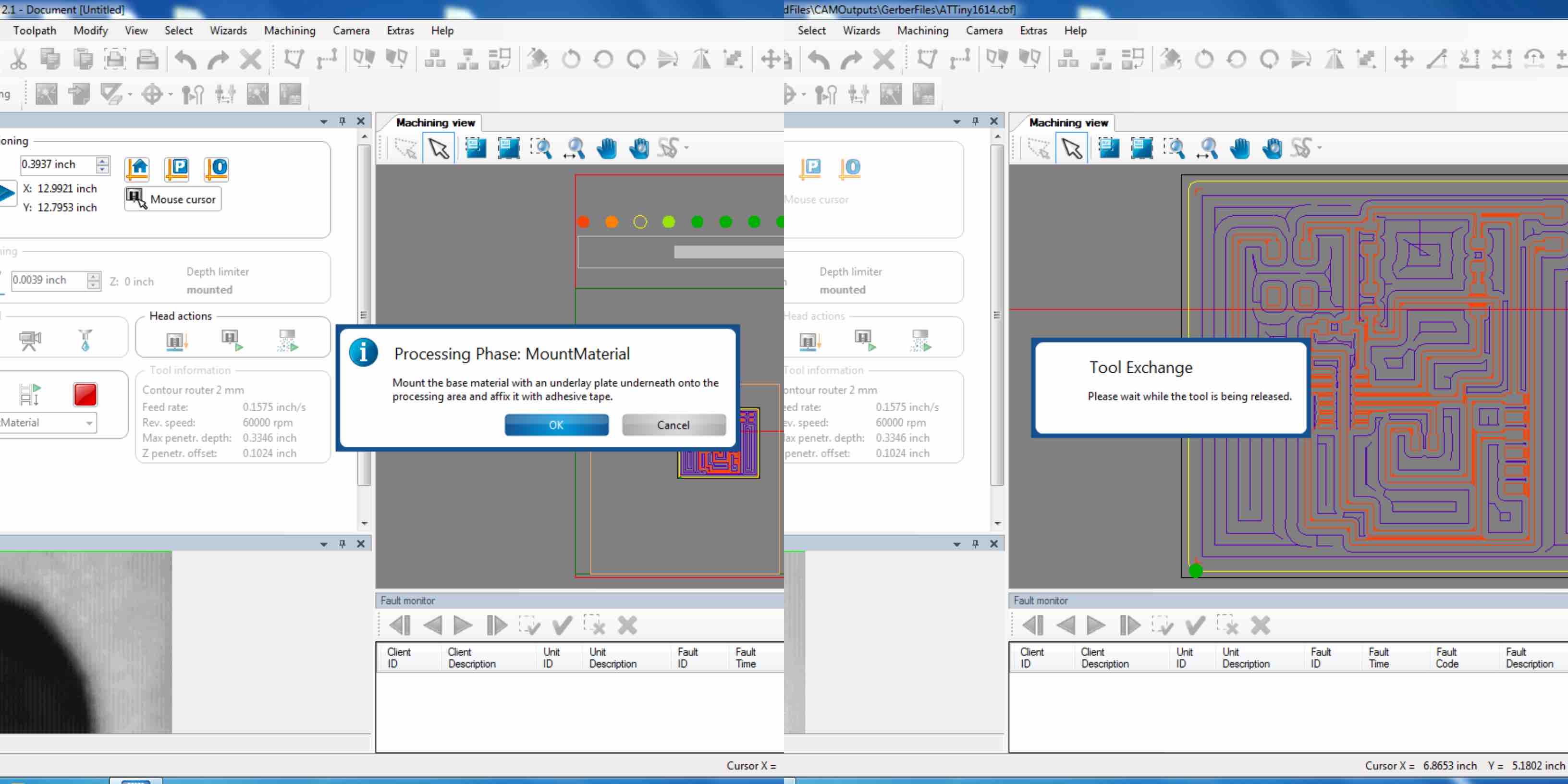
In our lab we have a small CNC Shotbot that can mill boards. However, we also have the LPKF available for electronics production. This is the mill the was used to cut the board for this assignment. Our local instructor provided us with an SOP to study before stepping us through the process. The LPKF Mill sits on a workstation with the monitor and computer set up the the left of the mill. The LPKF mill has a software that is unique to the use of the machine called Circuit Pro. The thumbnail is represented by a small blue milled board. When double clicked the icon will open the necessary program.
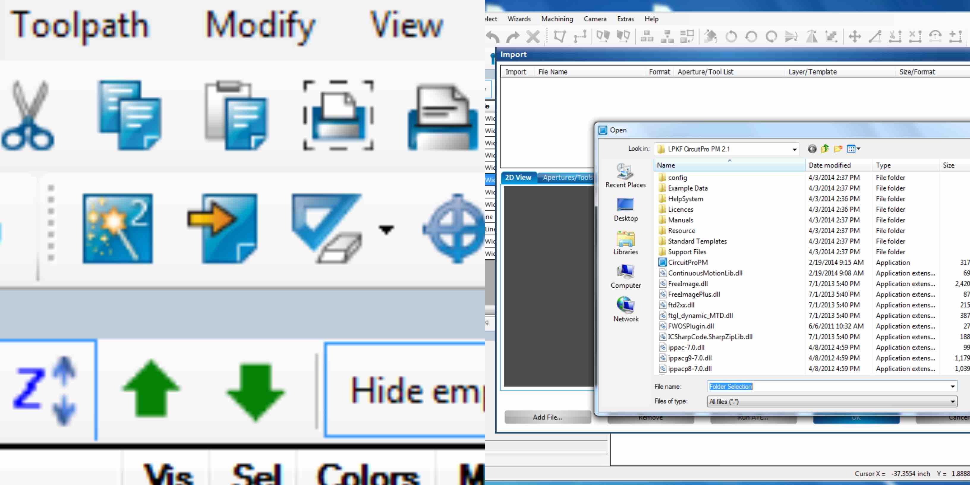
When the software is loaded open the next step is to load default template to start a new project. When the connection steps are through the software allows interaction. To import a nonnative format file find the yellow arrow over the blue rectangle with a corner folded up thumbnail and select this. This is an icon in the top tool bar of the program. This will open up the files located on the computer. Select the correct files associated with your board. I only needed to import my top board layout for the traces.
With the copper top layer imported I am able to start the set up process with the LPKF. In the CAM view of the board there will be a black background and red traces to represent the board design. Using the tool bar on the left hand side of the software there is a rectangle option. Select create rectangle. This will prompt a window to open up. An exact dimension can be typed in and applied by the axis specifications. However, I used the mouse and drew a rectangle directly around my desired traces. This changed the backing of my board to yellow to represent the size. The next step is to set the specifications for the Technology Dialog. Choose option 4 of 4 in the insulate option. This will produce a complete rubout, meaning it will remove any excess copper on the plate that is not being used.
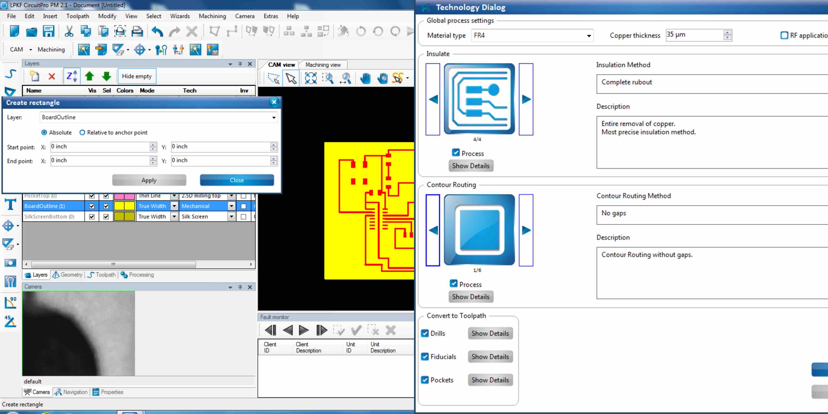
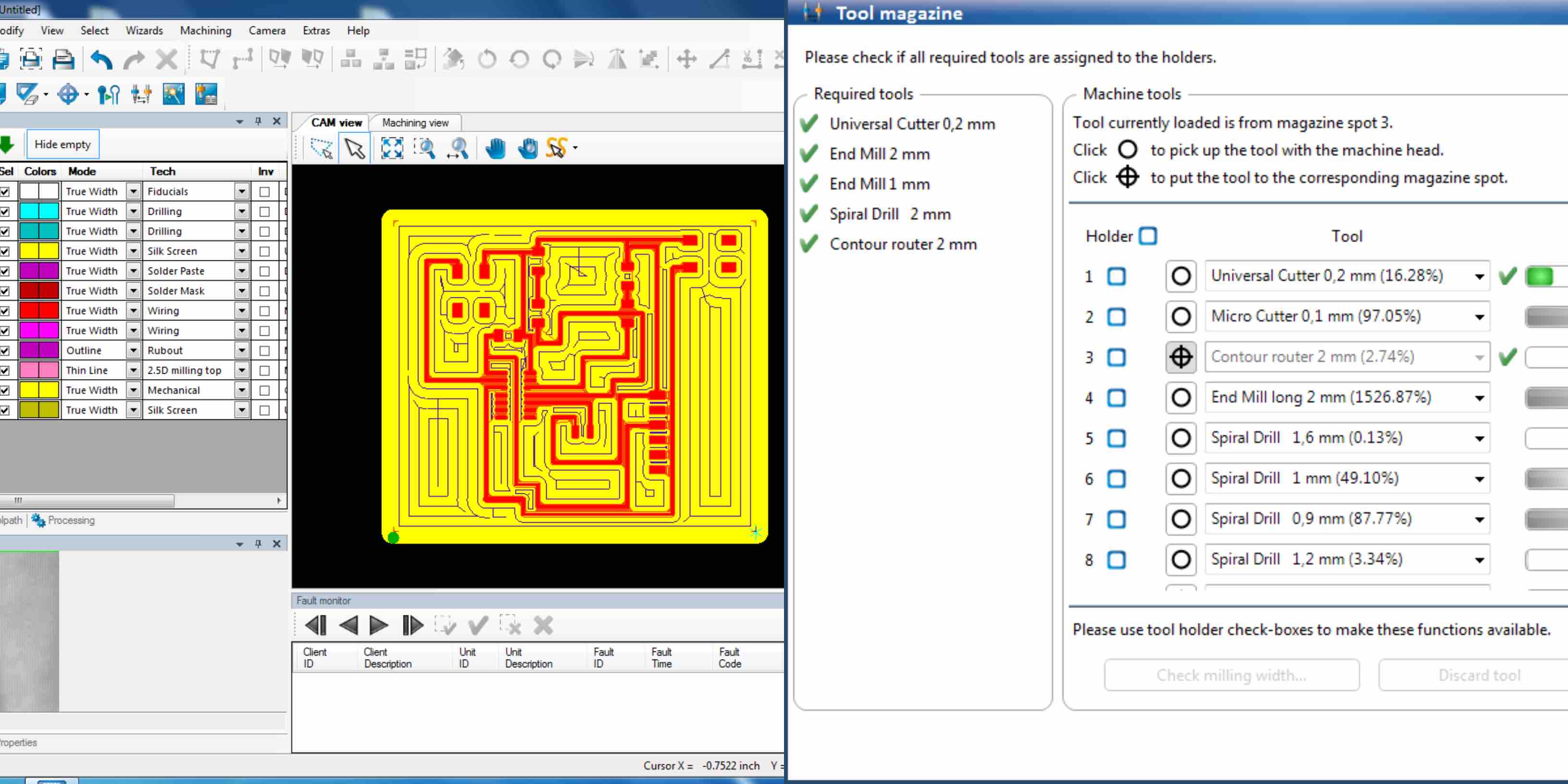
This will now show representations on the CAM view to show where the end mill will move to complete the rubout process. The tool magazine should then be checked to be sure the correct tools are in the machine to process the whole job. An end mill that lines the traces may be different then the one used for rubout, as well as the rubout end mill may be different from the end mill that cuts through the board as the final step.
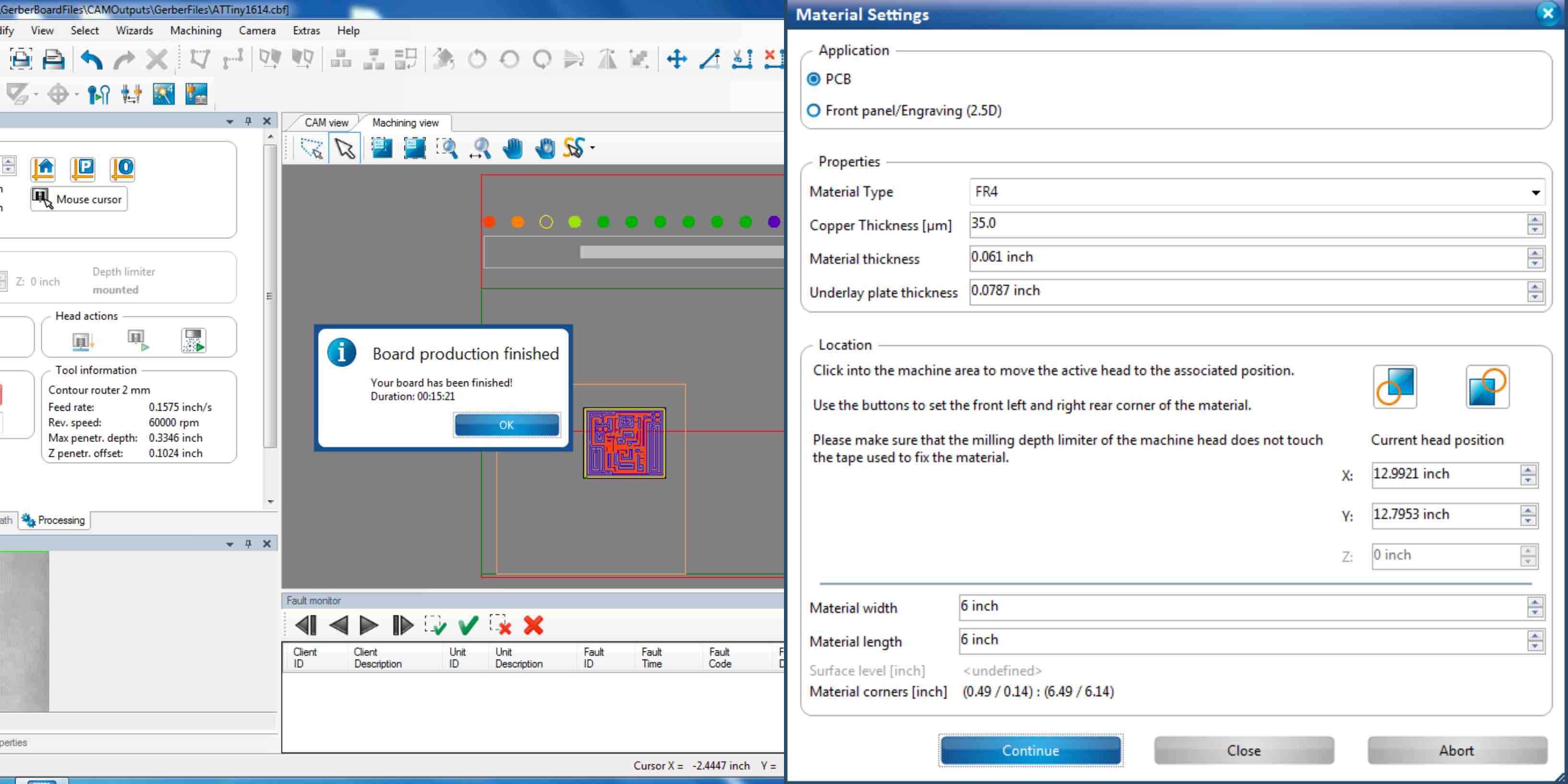
Once the end mills are set and checked the next settings are the material and the placement. In the material settings the PCB was selected to represent the material being used in the LPKF. Most other settings default into the program correctly, double checking for consistency. The material width and length are one of the important components to set. Being sure to match the material size of 6in by 6in. Providing this information to the machine will allow the LPKF to check placement. Checking the placement is important to be sure limited material waste. It will help to work around previous cuts, or to nest current cuts and optimize space available in the future.
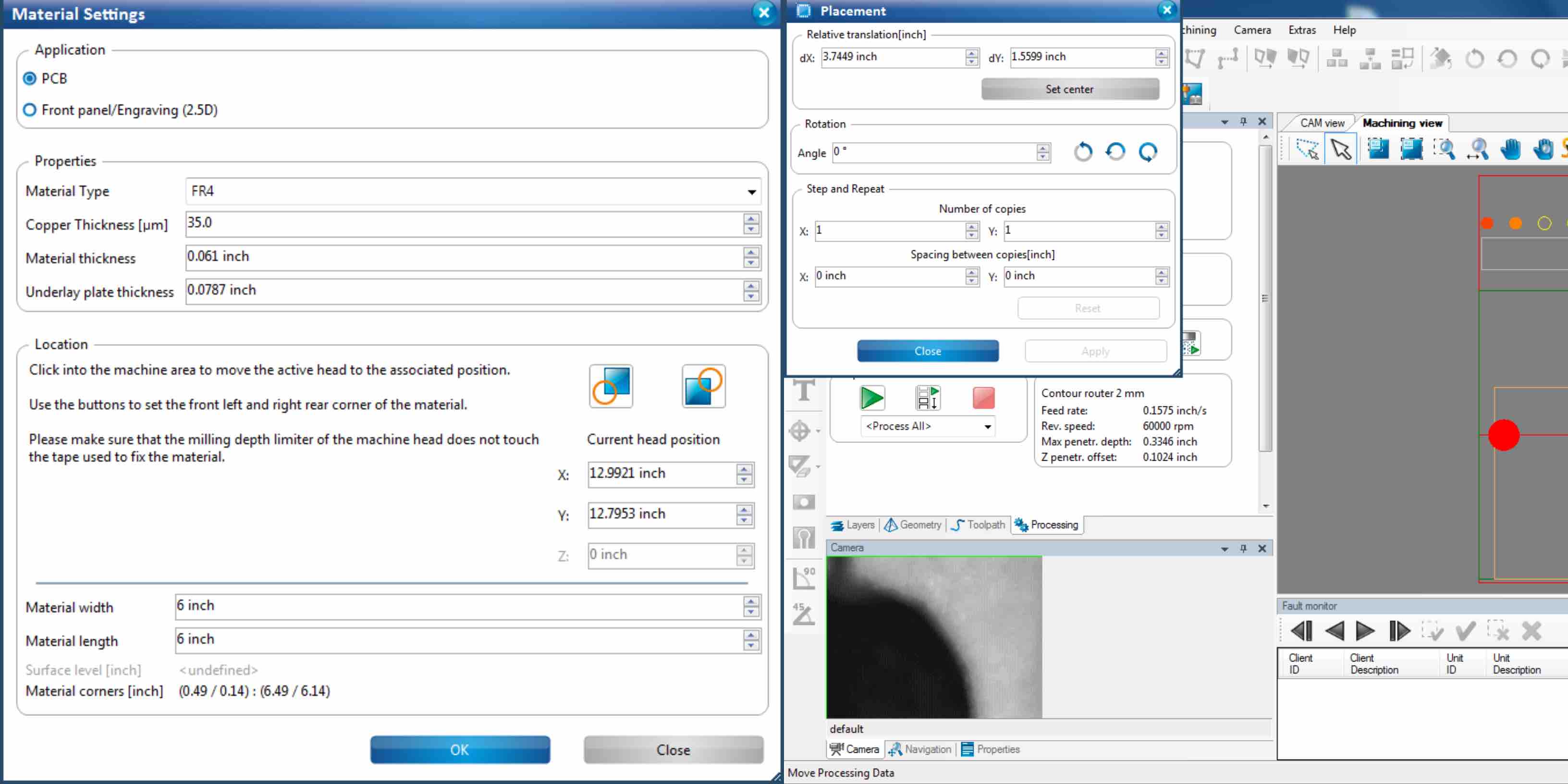
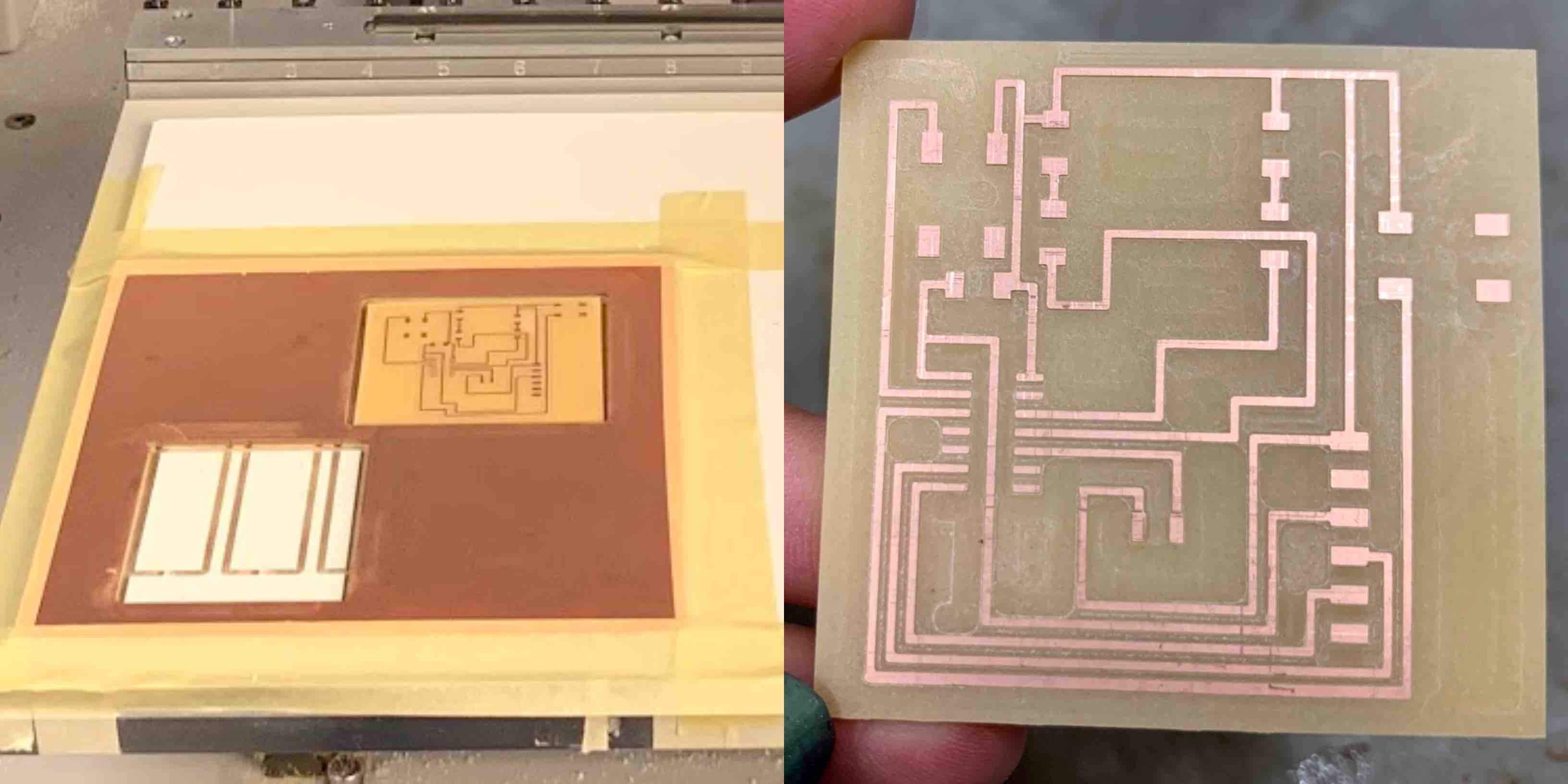
Once the placement is set and everything is aligned correctly the processing phase will begin. In the processing stage the LPKF will step the user through each necessary focus point. This will be a great way to double check that each component of the process is set correctly. Once each step is double checked for the optimal run the LPKF will begin the overall engraving and cutting process. The screen will prompt tool changes and the board production to track the process. Once finished the end mill will return to its home point, the lid can be lifted and the finished board can be removed. -Videos of the board being cut can be found below in the video gallery.
Soldering
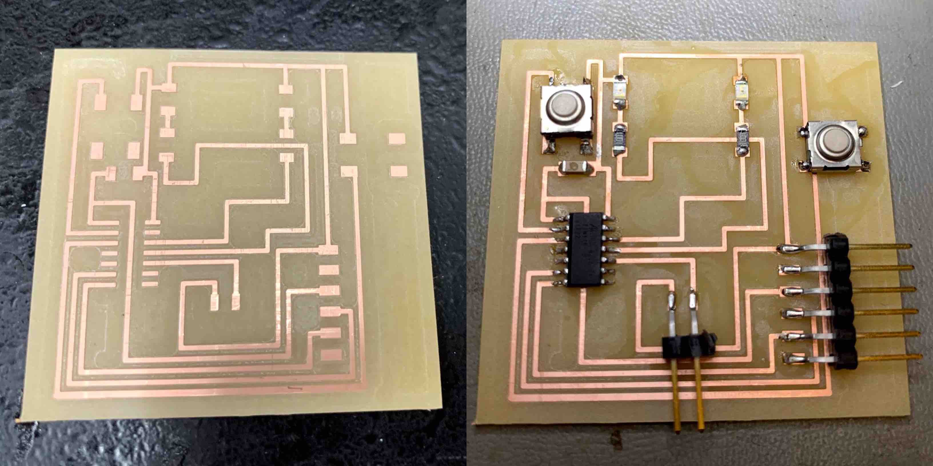
Once the board is milled the LPKF removes any remaining copper that is not necessary to the function of the board. With this complete the necessary connection can be seen based on the board you designed. The components only need connections at certain points. Those points are where the solder will connect them to the copper for flow of current. This means that the location of the components will line up with the copper pads that display the connection, however the copper that would lay under the component is removed in the milling process to be sure the current only travels where it should.
Before moving to the soldering station it is important to review your board schematic and collect the necessary components. This can be listed out onto a sheet of paper, with room for each component to be taped nest to the label. This helps to keep the user organized and be sure all correct components are collected. Located at each soldering station there is blue box with all needed supplies. Each station has a soldering kit and resting station. There is a needle tip bottle with flux to make it easy to apply. There is water and a sponge to dampen and use to keep the iron clean. Soldering in two sizes is available, the thinner solder being used to connect components to the board and thicker solder to store on the tip when the iron is not in use. There is also a microscope so that the user can see the small components and soldering pads as well.
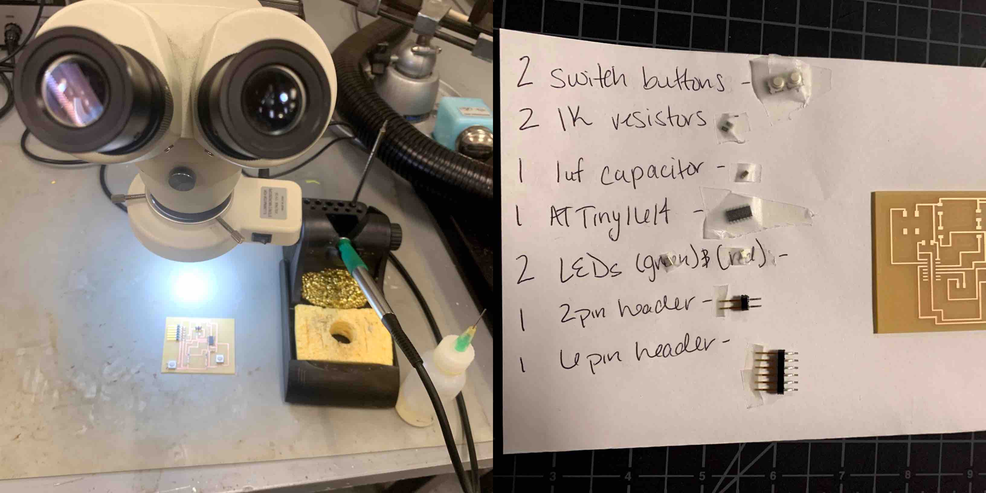
Now that the board is cut, the components collects and the soldering station turned on and heated up it is now time to begin the soldering process. With the board placed below the microscope it is important to decide what order you will solder the components. Some components can be harder to reach with others already in place. I have found that working from the inside of the board outward in a spiral motion has the best results. Starting with the components located to the inside of the board I removed them from the sheet of paper. As the component is placed in the correct location and the metal prongs are in connection with the copper pads it is to be soldered to, the user can drop a small amount of flux onto the component while holding it in place with the tweezers. With the iron now removed and in the dominate hand the user can hold the component in place with the tweezers. By connecting the iron to both the components metal prong and the copper pad, a one-two count will cause the flux to dissipate and the small amount of solder pre-applied to react and anchor one piece of the component to the board. With the component lightly anchored it will now be easier to being soldering. With the iron removed from the resting station and heated up fully, solder can be held by the other hand. The user can now rotate the board and begin working on the side that is not tacked down. This will help to increase the stability of the component when soldering. With the iron placed in contact with the components metal prong and the copper pad it will heat up anything it is in contact with. After a one-two count the surrounding areas should be hot enough to apply the tip of the metal solder. The solder will travel with the heat, so the user should be taking the correct steps to insure the solder is placed where intended. Once each different connecting of each component is soldered in place the construction of the board is finished.
Hero Shots
Testing for Function
Code Uploaded
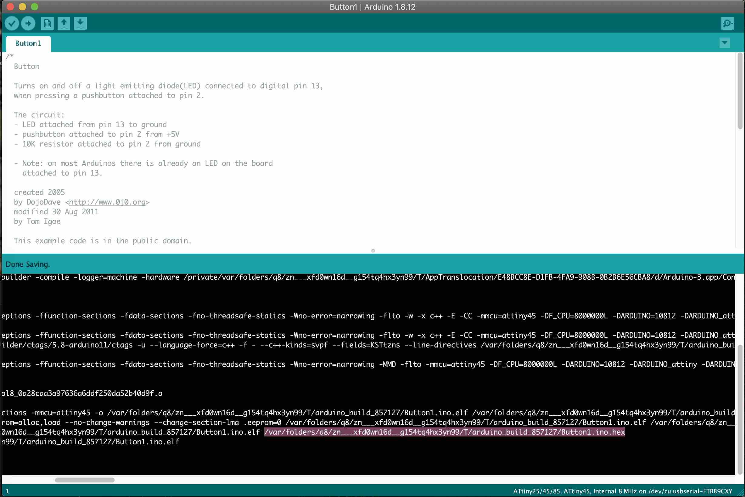
Below is the code used to program the ATTiny1614. I was able to use a code already created to understand how to work with the buttons and LEDs. I then changed the code in many different ways to create the final results.
/*
  Buttons

  Final code created 2020
  by alecia gorski
  combining multiple techniques to build from original base code. Code has changed.


  original code created 2005
  by DojoDave <http://www.0j0.org>
  modified 30 Aug 2011
  by Tom Igoe

  This example code is in the public domain.

  http://www.arduino.cc/en/Tutorial/Button
*/

// constants won't change. They're used here to set pin numbers:
const int buttonPin = 0;     // the number of the pushbutton pin
const int buttonPinB = 1;
const int ledPin =  8;      // the number of the LED pin
const int ledPinB = 9;

// variables will change:
int buttonState = 0;         // variable for reading the pushbutton status
int buttonStateB = 0;
int ledState = 1;
int ledStateB = 1;

void setup() {
  // initialize the LED pin as an output:
  pinMode(ledPin, OUTPUT);
  // initialize the pushbutton pin as an input:
  pinMode(buttonPin, INPUT);
    // initialize the LED pin as an output:
  pinMode(ledPinB, OUTPUT);
  // initialize the pushbutton pin as an input:
  pinMode(buttonPinB, INPUT);
}

void loop() {
  // read the state of the pushbutton value:
  buttonState = digitalRead(buttonPin);
  buttonStateB = digitalRead(buttonPinB);

  // check if the pushbutton is pressed. If it is, the buttonState is HIGH:
  if (buttonState == HIGH) {
    // turn LED on:
    digitalWrite(ledPin, LOW);
    digitalWrite(ledPinB, LOW);
 }

  else {
    // turn LED off:
    digitalWrite(ledPin, HIGH);
    digitalWrite(ledPinB, HIGH);
  }
}
Once the code is created it must be compiled. During the compiling process the code is translated into an .hex file. This file is very important when uploading the code.
Uploading Code
In order to upload the code to my hello board I had to use an FTDI cable. This cable connects my board to my computer in order to transmit the code. I also made an adapter to transfer data using a 6 pin header to a 2 pin header.
Referencing Neils video shown during the lesson and linked in the schedule page or can be found here, I uploaded the pyupdi program. I was able to then use my terminal to complete the uploading process. With the code written in Arduino I compiled the sketch. No problems found, I then used the .hex file location, highlighted and shown in the video, to apply to the command line. The command below was used to complete the programming and uploading process.
pyupdi.py -d tiny412 -c /dev/cu.usbserial-FTBB94GD -b 57600 -f /var/folders/q8/zn___xfd0wn16d__g164tq4hx3yn99/T/arduino_build_639321/OneButtonTwoLEDS.ino.hex -v
Final Results
With the program successfully uploaded I was able to interact with the button on the board and make both of the LEDs light up at once.
x
Addition In-Depth Documentation of the Process
ATTiny45 Practice
As mentioned above I stepped through this process in creating the ATTiny45 hello board. I am documenting my practice and attempt to become more familiar with the program outside of the assignment. I used Eagle to create the board. Pulling from the eagle inventory I was able to place all components into the schematic, wire and label them, as well as layout my overall board design and connections.
Complications
When designing my board in Eagle I was very unfamiliar at first. I was unfamiliar with the language of the board layout, design and software interface. The more time I spent in the program the greater my understanding became. However, when first creating the board I did not realize until after my board was cut and components soldered that I was missing the connection of transmitting and receiving that runs from the 6 pin header to the ATTiny1614. As frustrating as this was I then made my correction in Eagle and repeated the board production process. In the end I became more familiar with each process and have a stronger outcome and understanding. In the process I was able to better nest my components and create an overall smaller board.
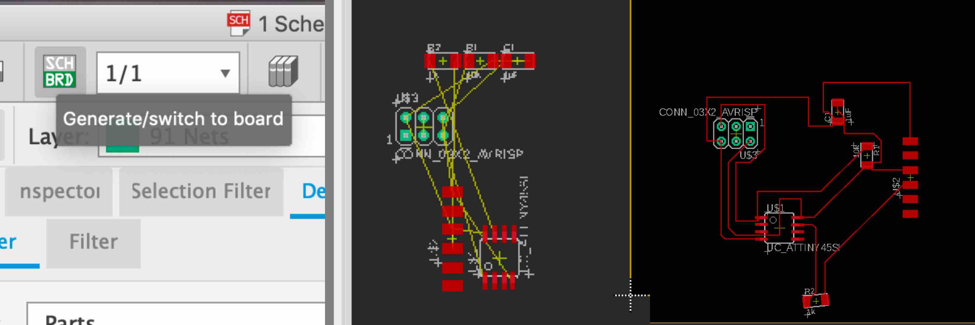
There was a complication I ran to outside if the redesign due to missed receiving and transmitting connection. This complication was confusing at first but then became very easily understood. This issue came to light when I received the error message listed below.
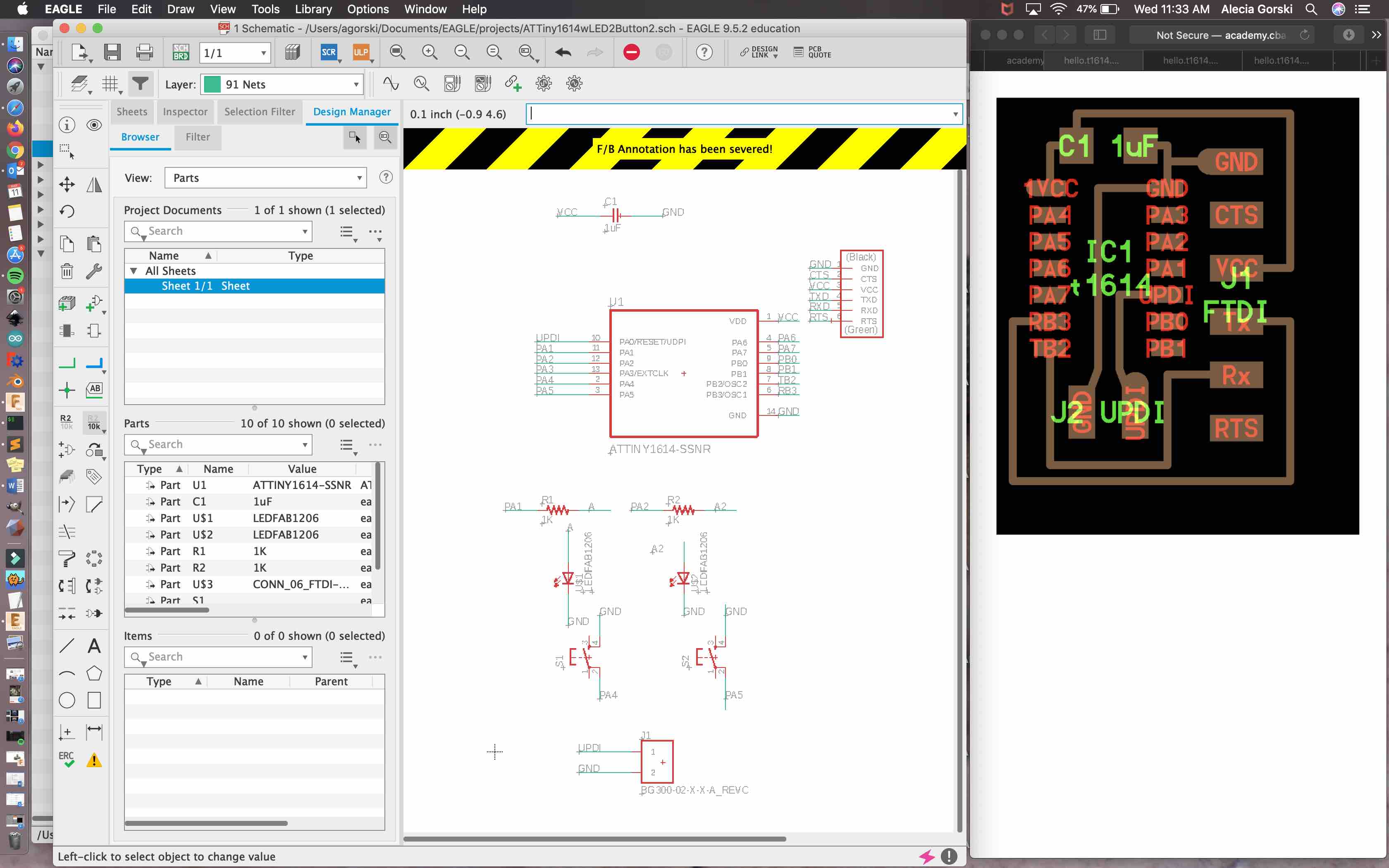
The message created a black and yellow stripped alert across the top of my working window. It then read F/B Annotation has been severed! This was broken down to mean that I had exited one of my working screens and it was no longer linked. When I closed my final board working window it then severed the connection to my schematic. Therefore, if I had made any schematic changes it would not have reflected into the final board layout. This was cleared up when I reopened my window. I made a change in my schematic and it reflected in my board layout.