Electronics Design
What are the electronic boards?
According to Wikipedia, A printed circuit board (PCB) mechanically supports and electrically connects electrical or electronic components using conductive tracks, pads and other features etched from one or more sheet layers of copper laminated onto and / or between sheet layers of a non-conductive substrate. Components are generally soldered onto the PCB to both electrically connect and mechanically fasten them to it. Printed circuit boards are used in all but the simplest electronic products. They are also used in some electrical products, such as passive switch boxes. Alternatives to PCBs include wire wrap and point-to-point construction, both once popular but now rarely used. PCBs require additional design effort to lay out the circuit, but manufacturing and assembly can be automated. Specialized CAD software is available to do much of the work of layout. Mass-producing circuits with PCBs is cheaper and faster than with other wiring methods, as components are mounted and wired in one operation. Large numbers of PCBs can be fabricated at the same time, and the layout only has to be done once. PCBs can also be made manually in small quantities, with reduced benefits. PCBs can be single-sided (one copper layer), double-sided (two copper layers on both sides of one substrate layer), or multi-layer (outer and inner layers of copper, alternating with layers of substrate). Multi-layer PCBs allow for much higher component density, because circuit traces on the inner layers would otherwise take up surface space between components. The rise in popularity of multilayer PCBs with more than two, and especially with more than four, copper planes was concurrent with the adoption of surface mount technology. However, multilayer PCBs make repair, analysis, and field modification of circuits much more difficult and usually impractical.
AutoDesk Eagle
Schematic
This week I worked on designing an electronic board through the Eagle program, where I designed the "Echo hello world" board as requested this week.
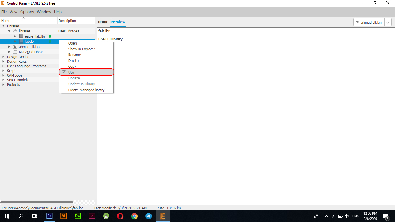
Initially, I downloaded the Fab library from the FabAcademy website, and installed the library in Eagle, To activate the library or add it to the program, we need to put it in the usage list as shown in the following image
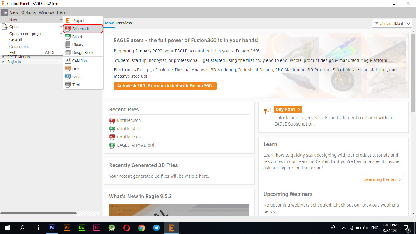
After I opened the program and installed the library, I opened a new file through "File - New - Schematic", and then I started adding the parts needed to make the electronic tablet.
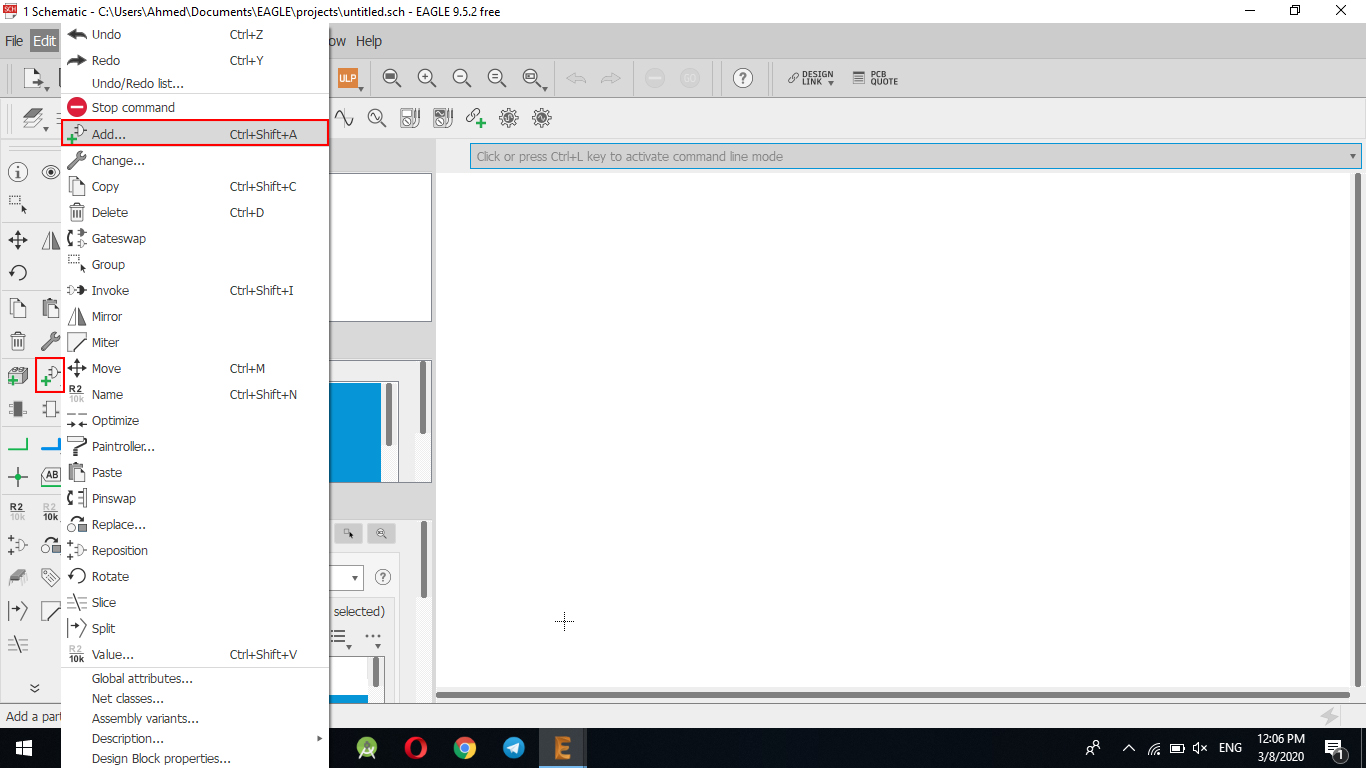
When opening the file, you started adding the pieces through "Edit - Add", or you can do this through the sidebar toolbar, where you can access the same option through this bar. I gathered the names of the pieces I would need while designing the tablet and started searching for them inside the Fab Library
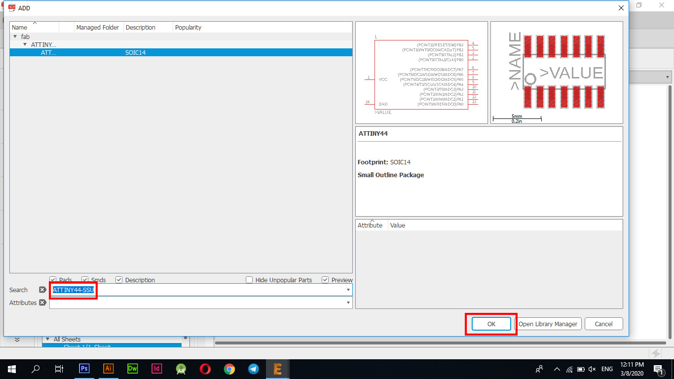
For your convenience, I searched directly for the pieces by typing the name assigned to them. For example, I only needed "ATTINY44-SSU". I typed the full name of the piece and the required piece will appear.
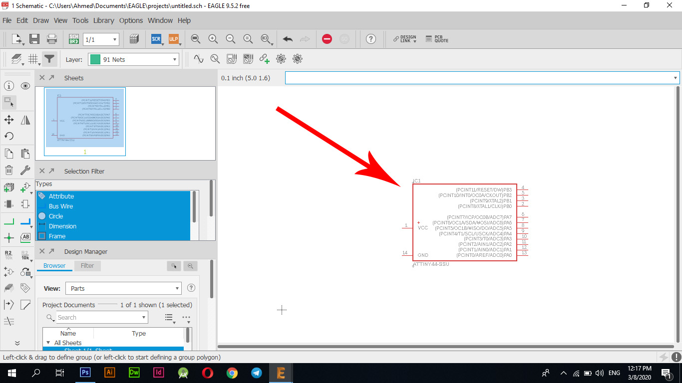
After I added the first piece and then completed adding the electronic parts to the electronic board, I also added the connections between the electronic parts and labels for each of the existing elements, I have read the book "Atmel board" to learn more about the delivery method and how to operate the electronic board.
The parts used in the electronic tablet
| Components | Lib | Footprint |
|---|---|---|
| ATTINY44-SSU | FAB | SOIC14 |
| 6MM_SWITCH | FAB | OMRON SWITCH |
| AVRISP | FAB | 2X03SMD |
| FTDI-SMD-HEADER | FAB | 1X06SMD |
| LED | FAB | LED1206FAB |
| RES-US | FAB | R1206FAB |
| RESONATOR | FAB | EFOBM |
| RES-US | FAB | R1206FAB |
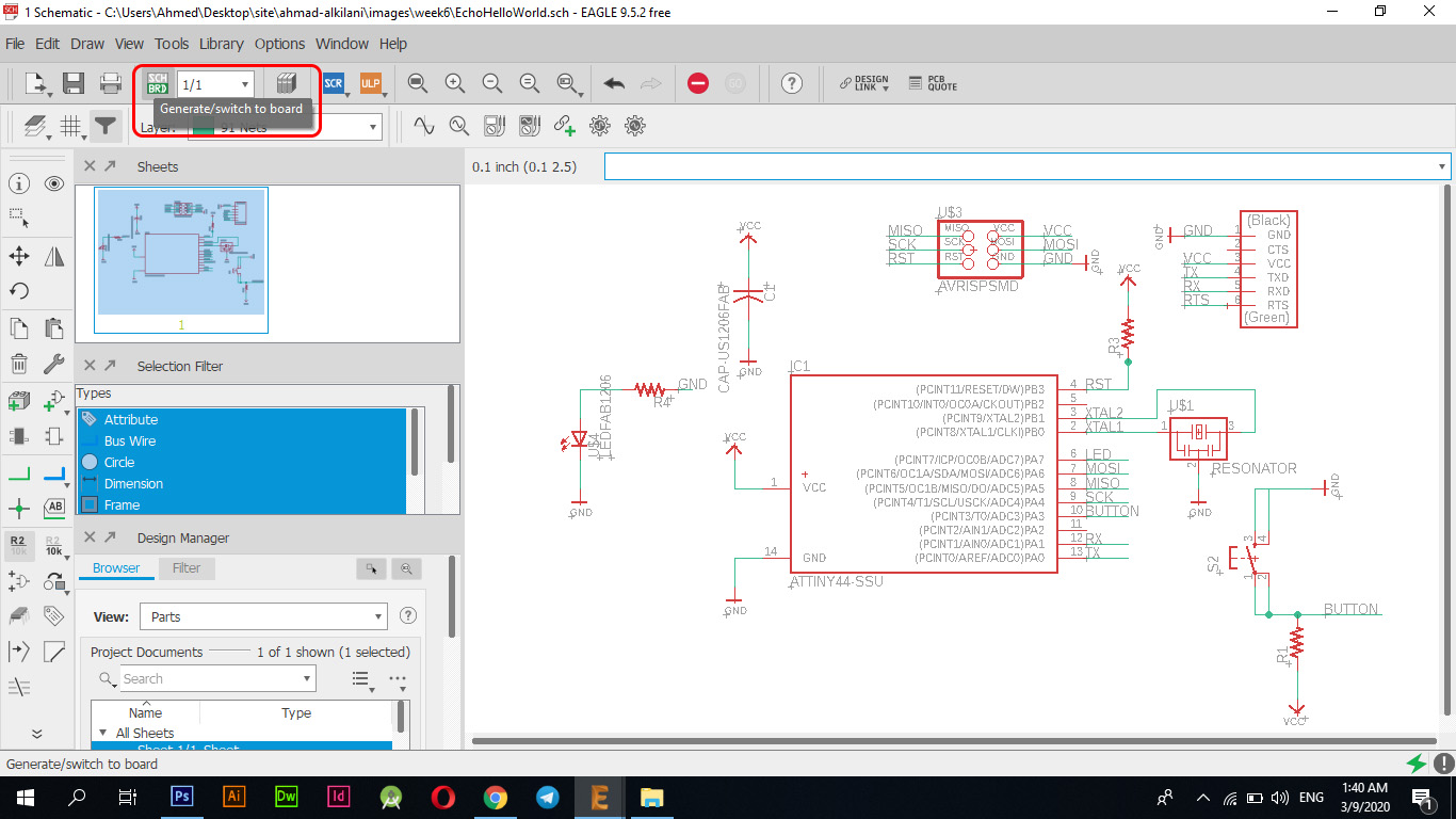
After I finished adding the pieces and nets between them, I moved to the second stage, which is connecting the parts between them and making sure that the design is free of errors and preparing the plate to be cut through the "PCB Roland Machine", so I moved to the interface of cutting the parts between them or what is known as a plate "Board" via the taskbar at the top as indicated in the image below.
Board
You moved the pieces to the task area through the "Move" option through the sidebar of the tools where you can click on any piece through the "+" button that is centered and begin to move it to the place you see fit for it.
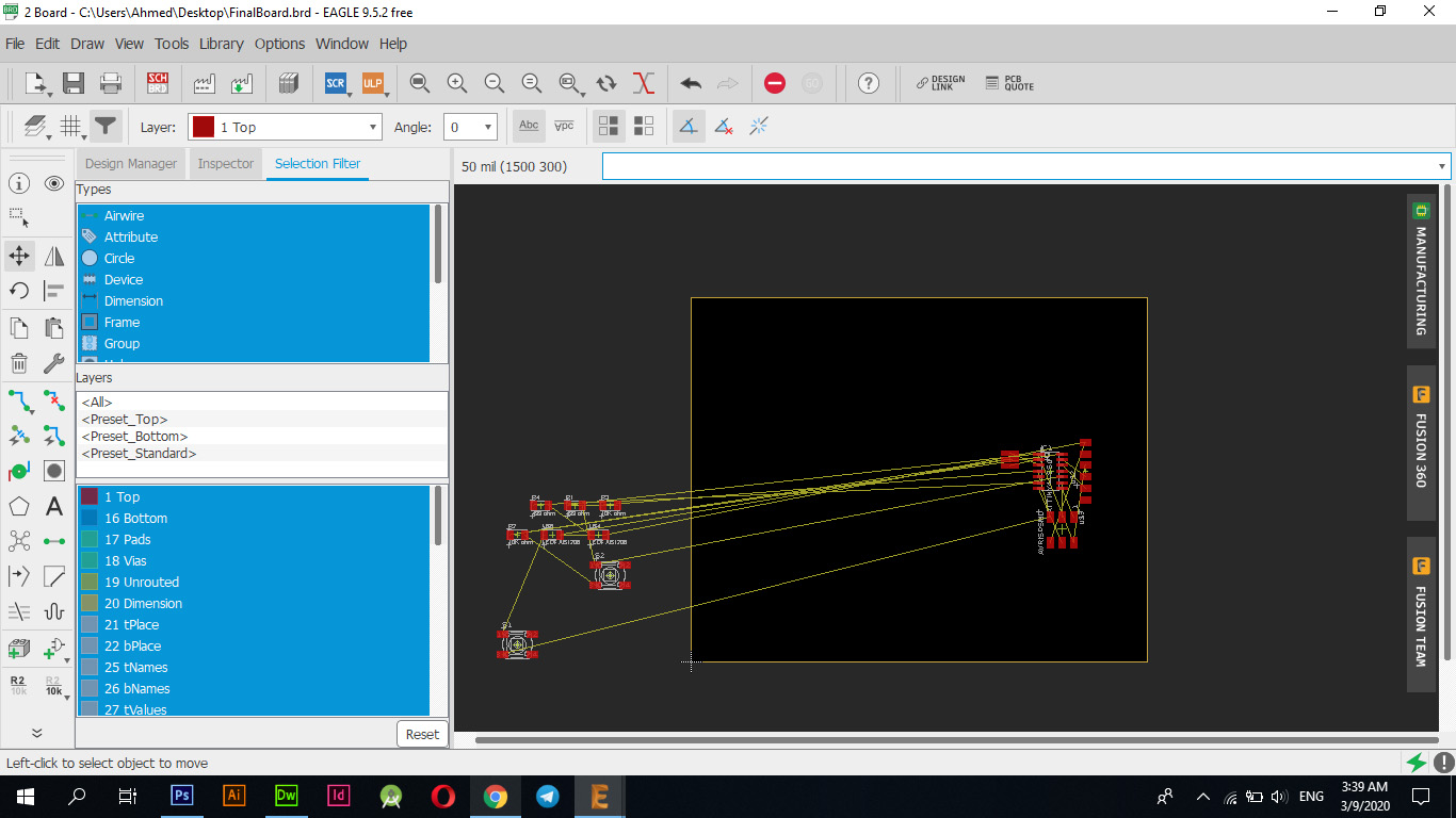
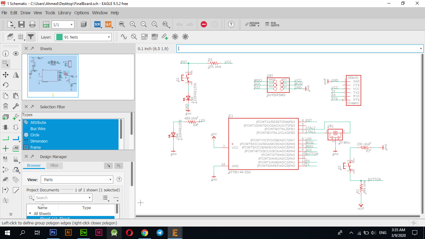
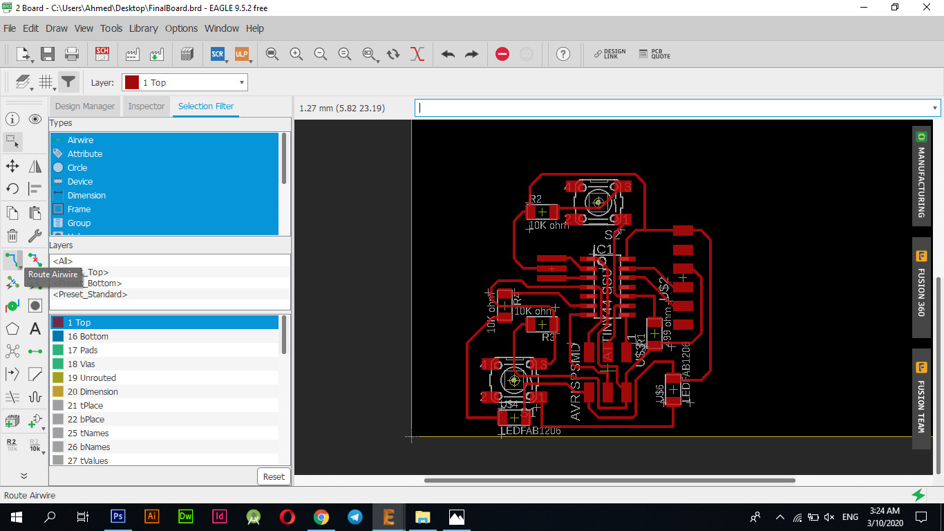
I put each part in the correct place so that it would be connected without any problems and as it appears in the following picture, this is the arrangement that I relied upon during the connection, but in the end I had to change the locations of some parts to be compatible with other connections and not be a barrier to other connections.
I used the "Route Airwire" option to connect between the available parts where I used some settings that I had to adjust to ensure that I make the appropriate connections for this process and these pictures show these settings where these settings work to adjust the font size between connections in the "Size" tab, while working The settings in the "Clearance" tab adjust the distance between the line and the other to ensure that the "Traces" are not affected during the cutting process.
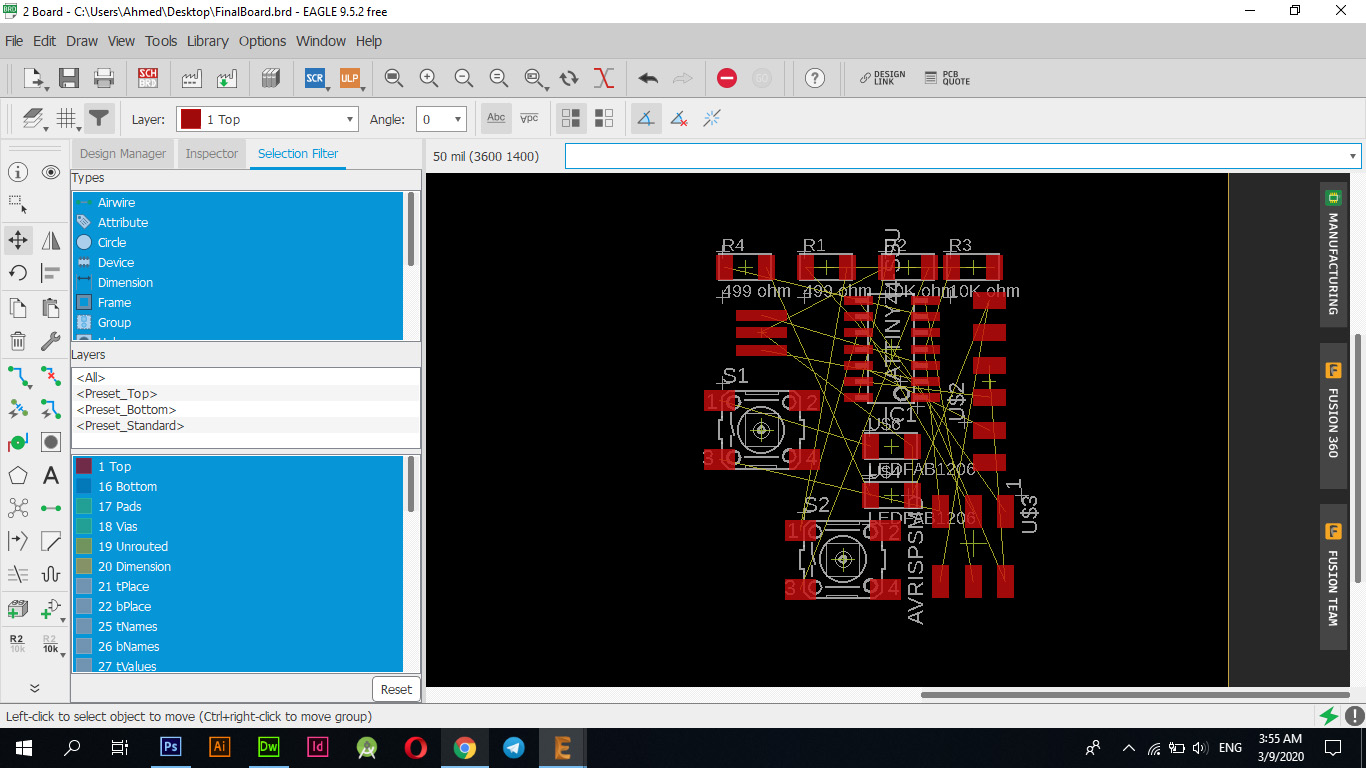
You have connected all parts together correctly as shown in the following picture
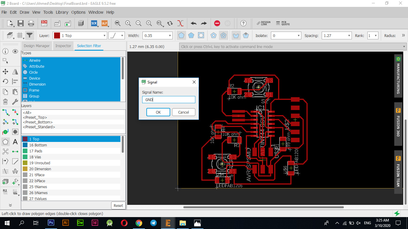
I used the "Polygn" tool to link the "GND" to the electronic board, where I drew a path around the tablet, and when finished I got a window where it indicates that the electronic tablet can be linked with "GND" knowing that it is not possible to link any other type only "GND" that is linked to this path .
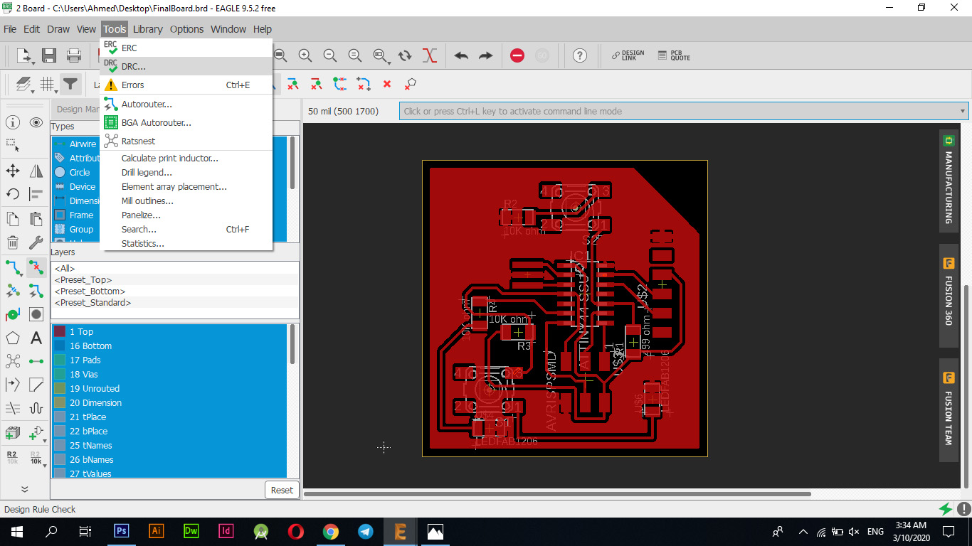
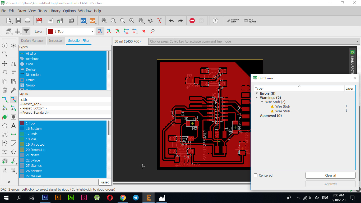
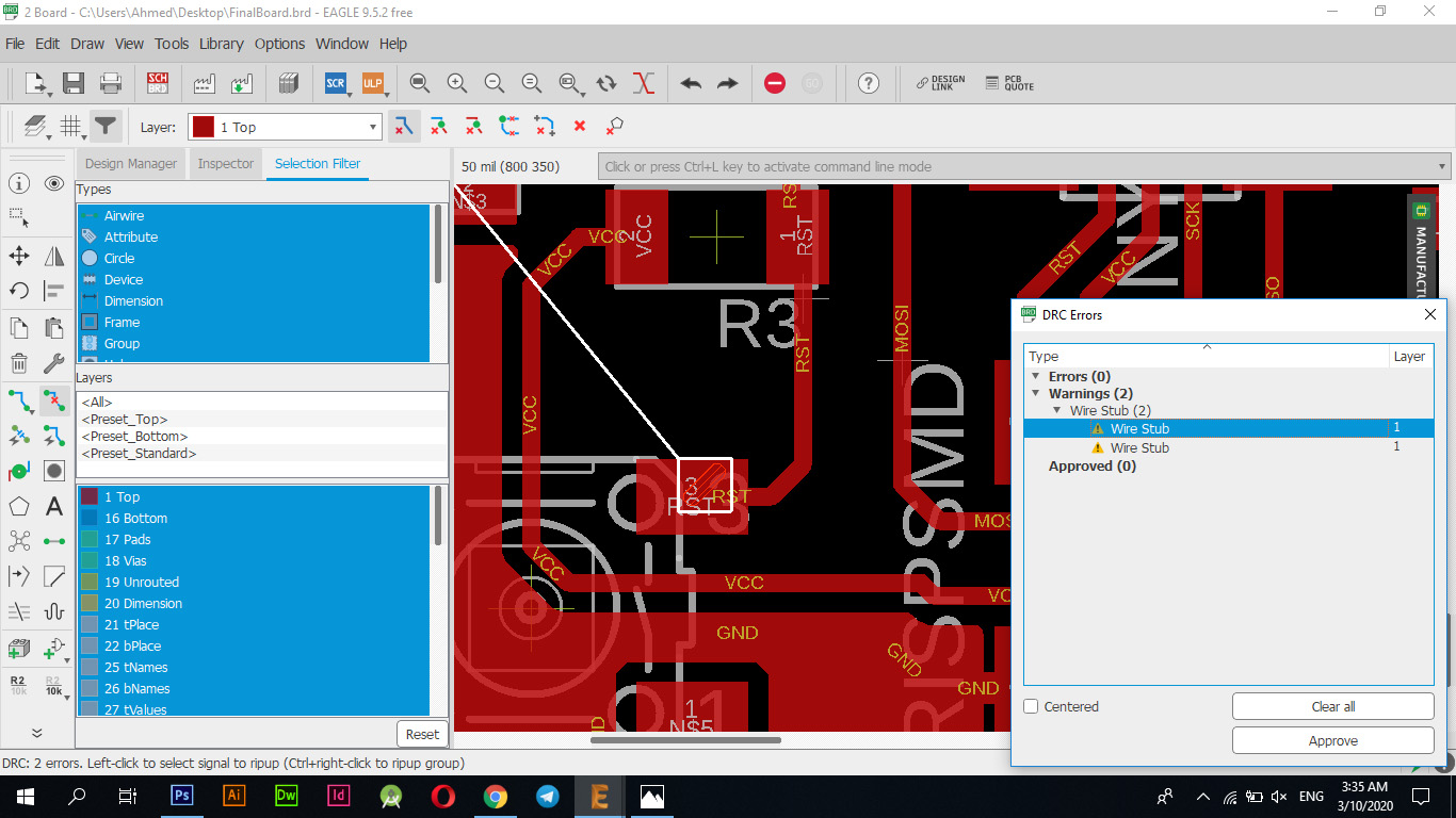
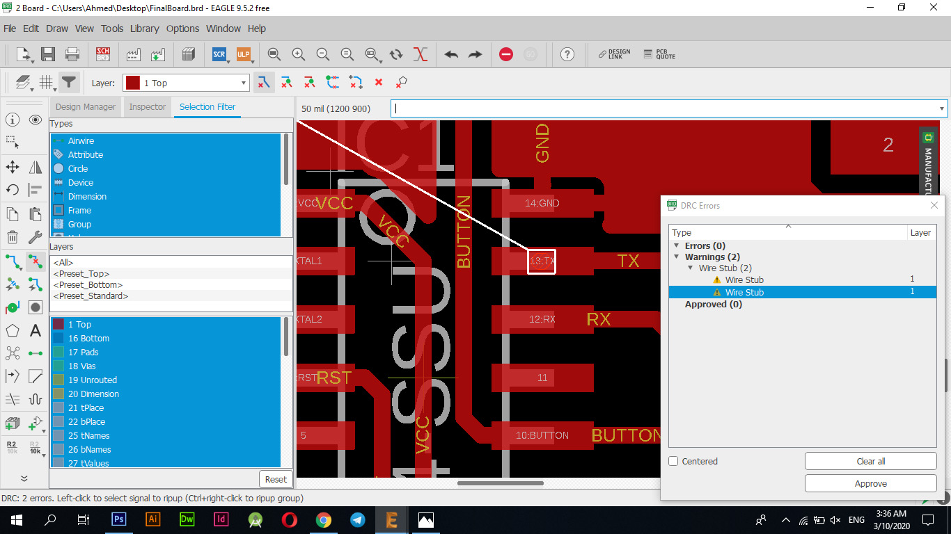
I have verified the errors and indeed I encountered two simple errors as I put more connections on the pieces themselves which sabotaged the pieces and removed the connections so I edged them and re-checked and indeed I skipped all the errors and finished designing and connecting in full, the pictures below show the nature of the errors that I encountered that with the "Delete" tool in the sidebar tool delete the extra and causing problems.
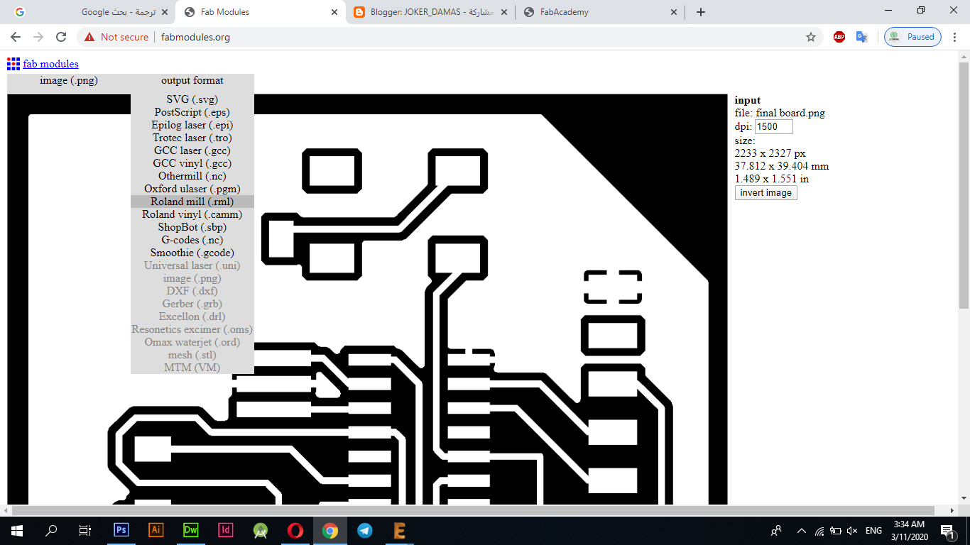
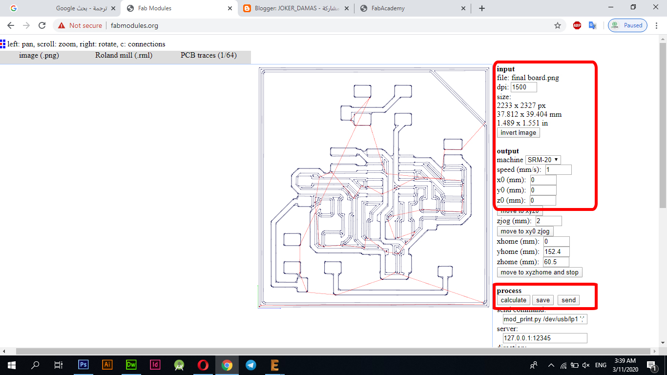
I exported the file in png format, as I made two files, one of them "Traces" and the other "OutLine" so that I could dig the tracks and cut the bezel.
Fab Modules
I opened the Fab Modules website and started setting up settings to prepare the tablet for cutting on a PCB machine.
Work steps:Open the FabModules website
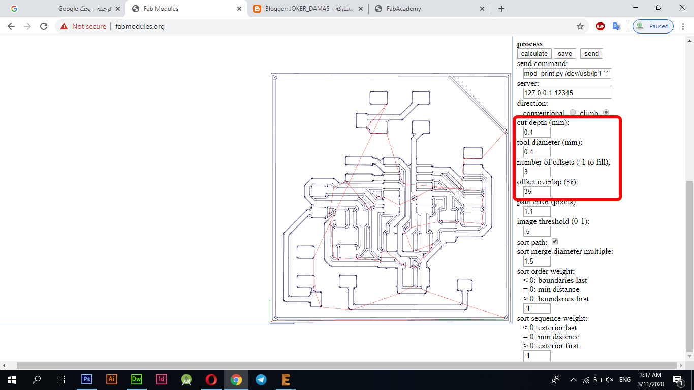
Traces Settings
| Mission | Size Or Type |
|---|---|
| dpi | 1500 |
| machine | SRM-20 |
| speed (mm/s) | 1 |
| x0 (mm) | 0 |
| y0 (mm) | 0 |
| z0 (mm) | 0 |
| cut depth (mm) | 0.1 |
| tool diameter (mm) | 0.4 |
| number of offsets (-1 to fill) | 4 |
| offset overlap (%) | 35 |
OutLine Settings
| Mission | Size Or Type |
|---|---|
| dpi | 1500 |
| machine | SRM-20 |
| speed (mm/s) | 1 |
| x0 (mm) | 0 |
| y0 (mm) | 0 |
| z0 (mm) | 0 |
| cut depth (mm) | 0.6 |
| stock thickness (mm) | 1.85 |
| tool diameter (mm) | 0.79 |
| number of offsets (-1 to fill) | 1 |
| offset overlap (%) | 35 |
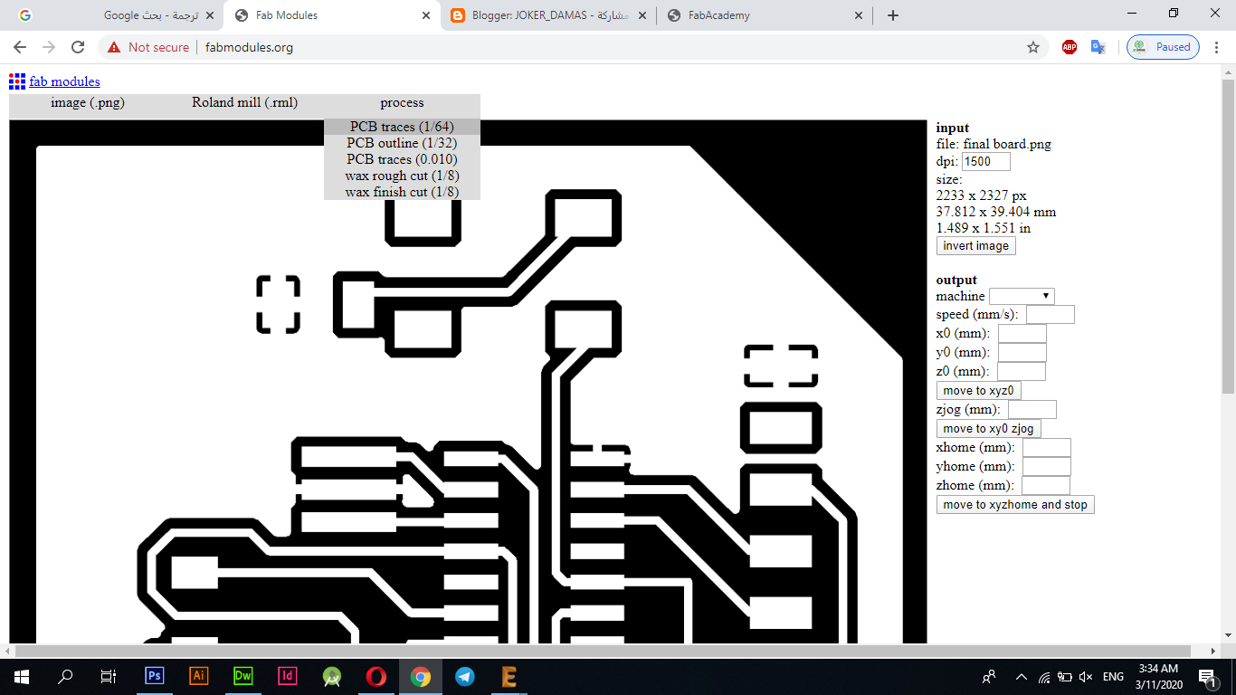
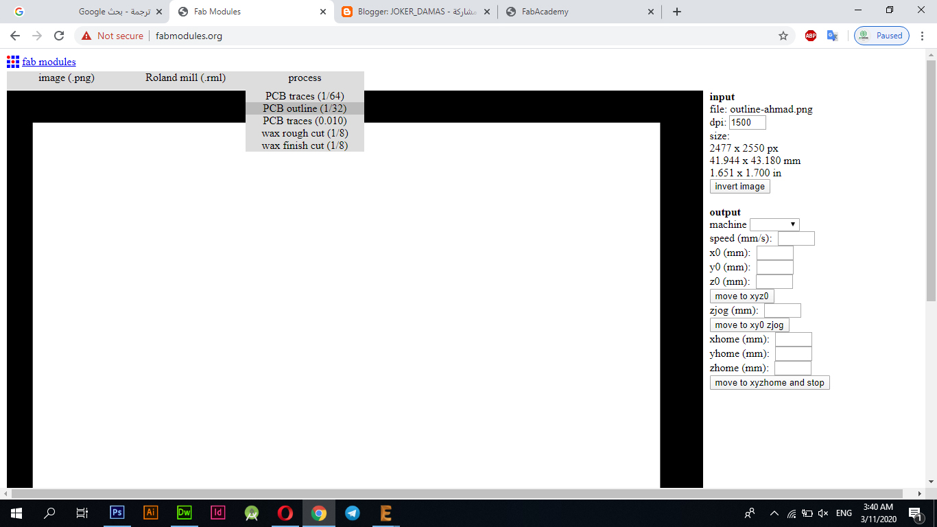
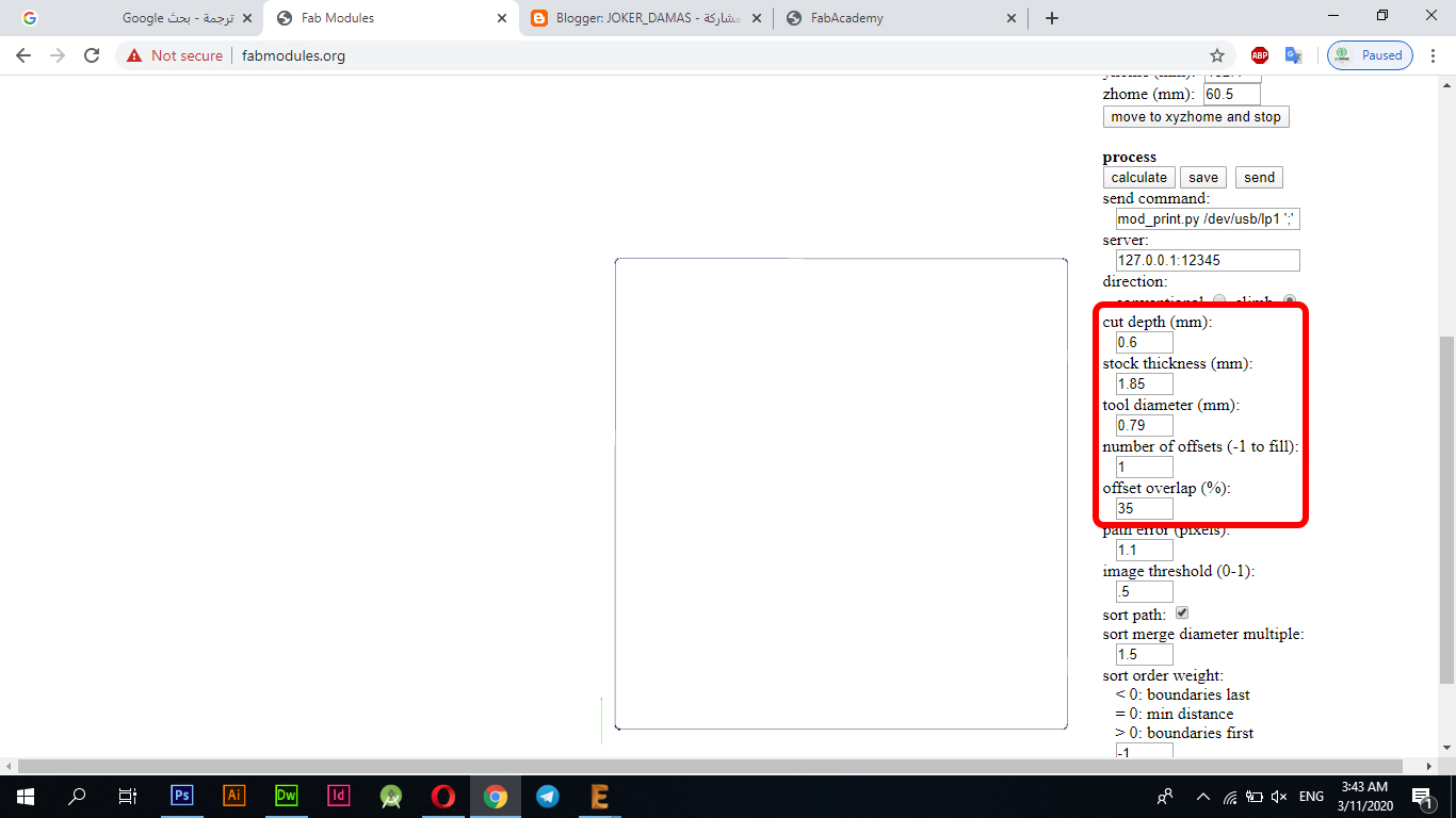
The image below shows the full settings for the storyboard clipping, where I included the "Traces" and "OutLine" settings.
Files - Open Source
ShematicBoard
Electronics Design
What are the electronic boards?
According to Wikipedia, A printed circuit board (PCB) mechanically supports and electrically connects electrical or electronic components using conductive tracks, pads and other features etched from one or more sheet layers of copper laminated onto and / or between sheet layers of a non-conductive substrate. Components are generally soldered onto the PCB to both electrically connect and mechanically fasten them to it. Printed circuit boards are used in all but the simplest electronic products. They are also used in some electrical products, such as passive switch boxes. Alternatives to PCBs include wire wrap and point-to-point construction, both once popular but now rarely used. PCBs require additional design effort to lay out the circuit, but manufacturing and assembly can be automated. Specialized CAD software is available to do much of the work of layout. Mass-producing circuits with PCBs is cheaper and faster than with other wiring methods, as components are mounted and wired in one operation. Large numbers of PCBs can be fabricated at the same time, and the layout only has to be done once. PCBs can also be made manually in small quantities, with reduced benefits. PCBs can be single-sided (one copper layer), double-sided (two copper layers on both sides of one substrate layer), or multi-layer (outer and inner layers of copper, alternating with layers of substrate). Multi-layer PCBs allow for much higher component density, because circuit traces on the inner layers would otherwise take up surface space between components. The rise in popularity of multilayer PCBs with more than two, and especially with more than four, copper planes was concurrent with the adoption of surface mount technology. However, multilayer PCBs make repair, analysis, and field modification of circuits much more difficult and usually impractical.
AutoDesk Eagle
Schematic
This week I worked on designing an electronic board through the Eagle program, where I designed the "Echo hello world" board as requested this week.
Initially, I downloaded the Fab library from the FabAcademy website, and installed the library in Eagle, To activate the library or add it to the program, we need to put it in the usage list as shown in the following image
After I opened the program and installed the library, I opened a new file through "File - New - Schematic", and then I started adding the parts needed to make the electronic tablet.
When opening the file, you started adding the pieces through "Edit - Add", or you can do this through the sidebar toolbar, where you can access the same option through this bar. I gathered the names of the pieces I would need while designing the tablet and started searching for them inside the Fab Library
For your convenience, I searched directly for the pieces by typing the name assigned to them. For example, I only needed "ATTINY44-SSU". I typed the full name of the piece and the required piece will appear.
After I added the first piece and then completed adding the electronic parts to the electronic board, I also added the connections between the electronic parts and labels for each of the existing elements, I have read the book "Atmel board" to learn more about the delivery method and how to operate the electronic board.
The parts used in the electronic tablet
| Components | Lib | Footprint |
|---|---|---|
| ATTINY44-SSU | FAB | SOIC14 |
| 6MM_SWITCH | FAB | OMRON SWITCH |
| AVRISP | FAB | 2X03SMD |
| FTDI-SMD-HEADER | FAB | 1X06SMD |
| LED | FAB | LED1206FAB |
| RES-US | FAB | R1206FAB |
| RESONATOR | FAB | EFOBM |
| RES-US | FAB | R1206FAB |
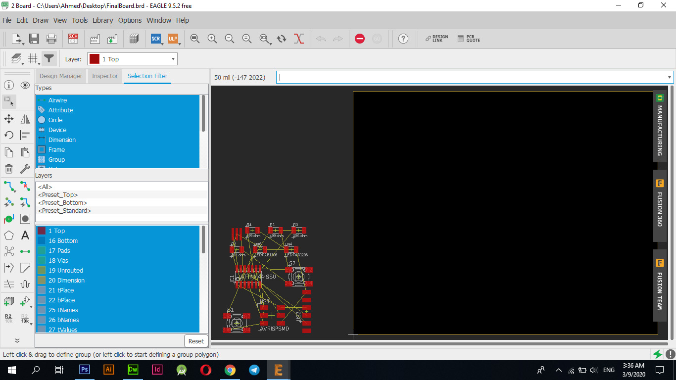
After I finished adding the pieces and nets between them, I moved to the second stage, which is connecting the parts between them and making sure that the design is free of errors and preparing the plate to be cut through the "PCB Roland Machine", so I moved to the interface of cutting the parts between them or what is known as a plate "Board" via the taskbar at the top as indicated in the image below.
Board
You moved the pieces to the task area through the "Move" option through the sidebar of the tools where you can click on any piece through the "+" button that is centered and begin to move it to the place you see fit for it.
I put each part in the correct place so that it would be connected without any problems and as it appears in the following picture, this is the arrangement that I relied upon during the connection, but in the end I had to change the locations of some parts to be compatible with other connections and not be a barrier to other connections.
I used the "Route Airwire" option to connect between the available parts where I used some settings that I had to adjust to ensure that I make the appropriate connections for this process and these pictures show these settings where these settings work to adjust the font size between connections in the "Size" tab, while working The settings in the "Clearance" tab adjust the distance between the line and the other to ensure that the "Traces" are not affected during the cutting process.
You have connected all parts together correctly as shown in the following picture
I used the "Polygn" tool to link the "GND" to the electronic board, where I drew a path around the tablet, and when finished I got a window where it indicates that the electronic tablet can be linked with "GND" knowing that it is not possible to link any other type only "GND" that is linked to this path .
I have verified the errors and indeed I encountered two simple errors as I put more connections on the pieces themselves which sabotaged the pieces and removed the connections so I edged them and re-checked and indeed I skipped all the errors and finished designing and connecting in full, the pictures below show the nature of the errors that I encountered that with the "Delete" tool in the sidebar tool delete the extra and causing problems.
I exported the file in png format, as I made two files, one of them "Traces" and the other "OutLine" so that I could dig the tracks and cut the bezel.
Fab Modules
I opened the Fab Modules website and started setting up settings to prepare the tablet for cutting on a PCB machine.
Work steps:Open the FabModules website
Traces Settings
| Mission | Size Or Type |
|---|---|
| dpi | 1500 |
| machine | SRM-20 |
| speed (mm/s) | 1 |
| x0 (mm) | 0 |
| y0 (mm) | 0 |
| z0 (mm) | 0 |
| cut depth (mm) | 0.1 |
| tool diameter (mm) | 0.4 |
| number of offsets (-1 to fill) | 4 |
| offset overlap (%) | 35 |
OutLine Settings
| Mission | Size Or Type |
|---|---|
| dpi | 1500 |
| machine | SRM-20 |
| speed (mm/s) | 1 |
| x0 (mm) | 0 |
| y0 (mm) | 0 |
| z0 (mm) | 0 |
| cut depth (mm) | 0.6 |
| stock thickness (mm) | 1.85 |
| tool diameter (mm) | 0.79 |
| number of offsets (-1 to fill) | 1 |
| offset overlap (%) | 35 |
The image below shows the full settings for the storyboard clipping, where I included the "Traces" and "OutLine" settings.
Files - Open Source
Shematic & BoardWhat are the electronic boards?
According to Wikipedia, A printed circuit board (PCB) mechanically supports and electrically connects electrical or electronic components using conductive tracks, pads and other features etched from one or more sheet layers of copper laminated onto and / or between sheet layers of a non-conductive substrate. Components are generally soldered onto the PCB to both electrically connect and mechanically fasten them to it. Printed circuit boards are used in all but the simplest electronic products. They are also used in some electrical products, such as passive switch boxes. Alternatives to PCBs include wire wrap and point-to-point construction, both once popular but now rarely used. PCBs require additional design effort to lay out the circuit, but manufacturing and assembly can be automated. Specialized CAD software is available to do much of the work of layout. Mass-producing circuits with PCBs is cheaper and faster than with other wiring methods, as components are mounted and wired in one operation. Large numbers of PCBs can be fabricated at the same time, and the layout only has to be done once. PCBs can also be made manually in small quantities, with reduced benefits. PCBs can be single-sided (one copper layer), double-sided (two copper layers on both sides of one substrate layer), or multi-layer (outer and inner layers of copper, alternating with layers of substrate). Multi-layer PCBs allow for much higher component density, because circuit traces on the inner layers would otherwise take up surface space between components. The rise in popularity of multilayer PCBs with more than two, and especially with more than four, copper planes was concurrent with the adoption of surface mount technology. However, multilayer PCBs make repair, analysis, and field modification of circuits much more difficult and usually impractical.
SCH - Schematic
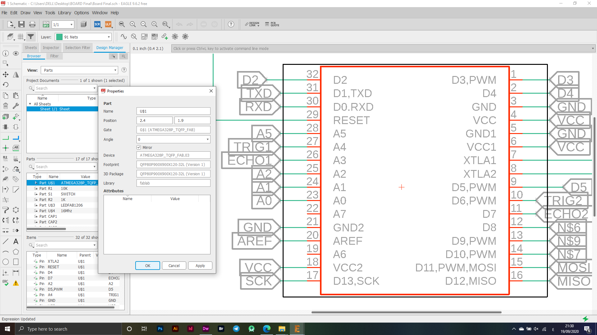
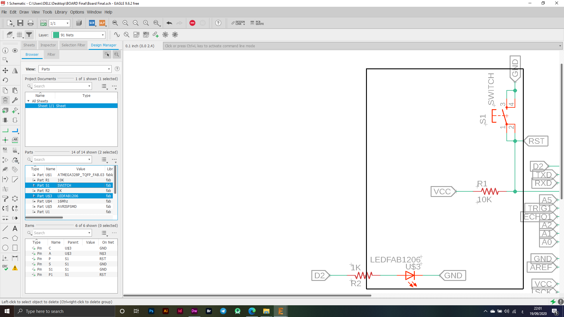
Depending on what the final project requires, I designed the electronic board for my project, and relied on AutoDesk Eagle to design the electronic board, first specifying the pieces that I will use in my final project and then moving on to Eagle for designing the electronic board.
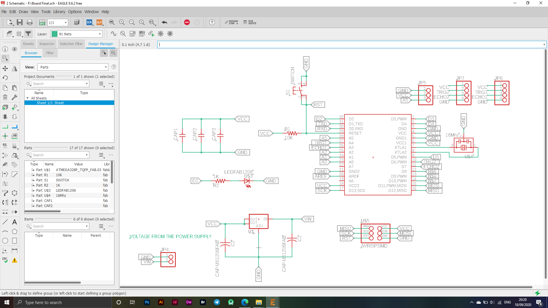
The image above shows the parts used in designing the electronic board for my final project. I used the main piece on which the electronic board "ATMEGA328P_TQFP_FAB.03" relies heavily on the microcontroller.
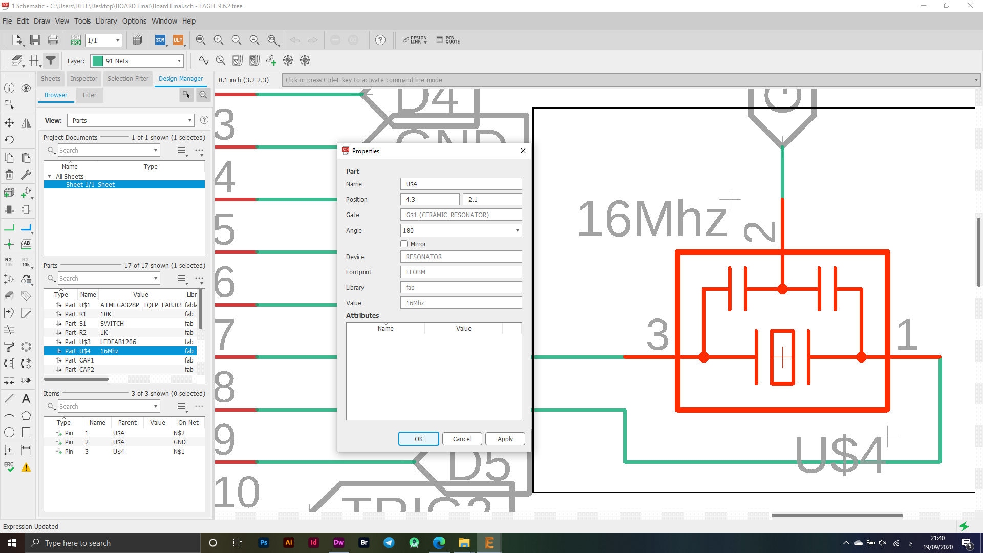
A resonant circuit is a device or circuit that produces resonance. And it naturally oscillates at some frequencies called its resonant frequency. This is because it resonates profusely on this frequency more than on other vibrations. While some programming things happen inside the microcontroller, it depends on this signal that will arrive from this piece.
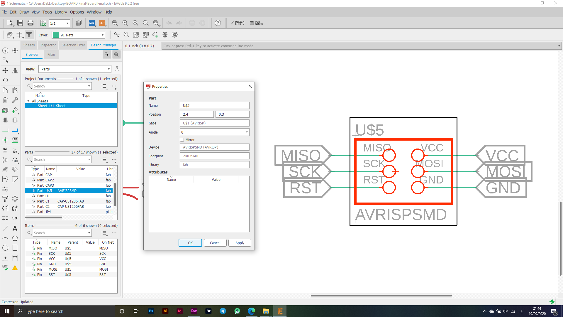
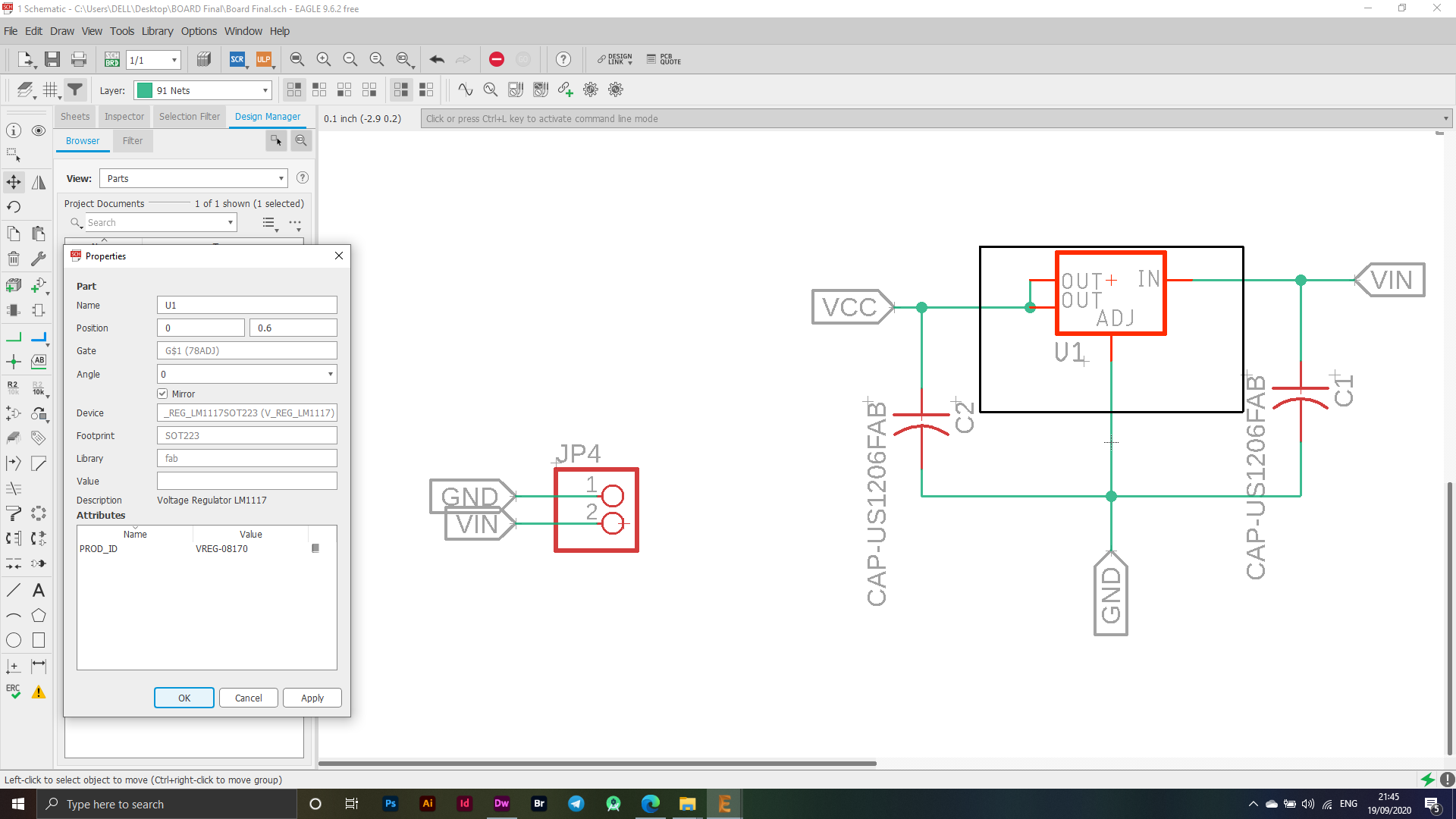
I have added an AVRISPSMD segment to be able to do programming for the ATMEGA microcontroller.
I have been thinking about the power source in my electronic board and found that using a Volatage Regulator is the best solution to support the electronic board with power with a power supply as I used this piece for the purpose of delivering energy within certain limits and converting the electricity that reaches the electronic board from electricity at high values to a specified value on Charging 5V so the power supply will convert the electricity that reaches the electronic board from "AC - DC".
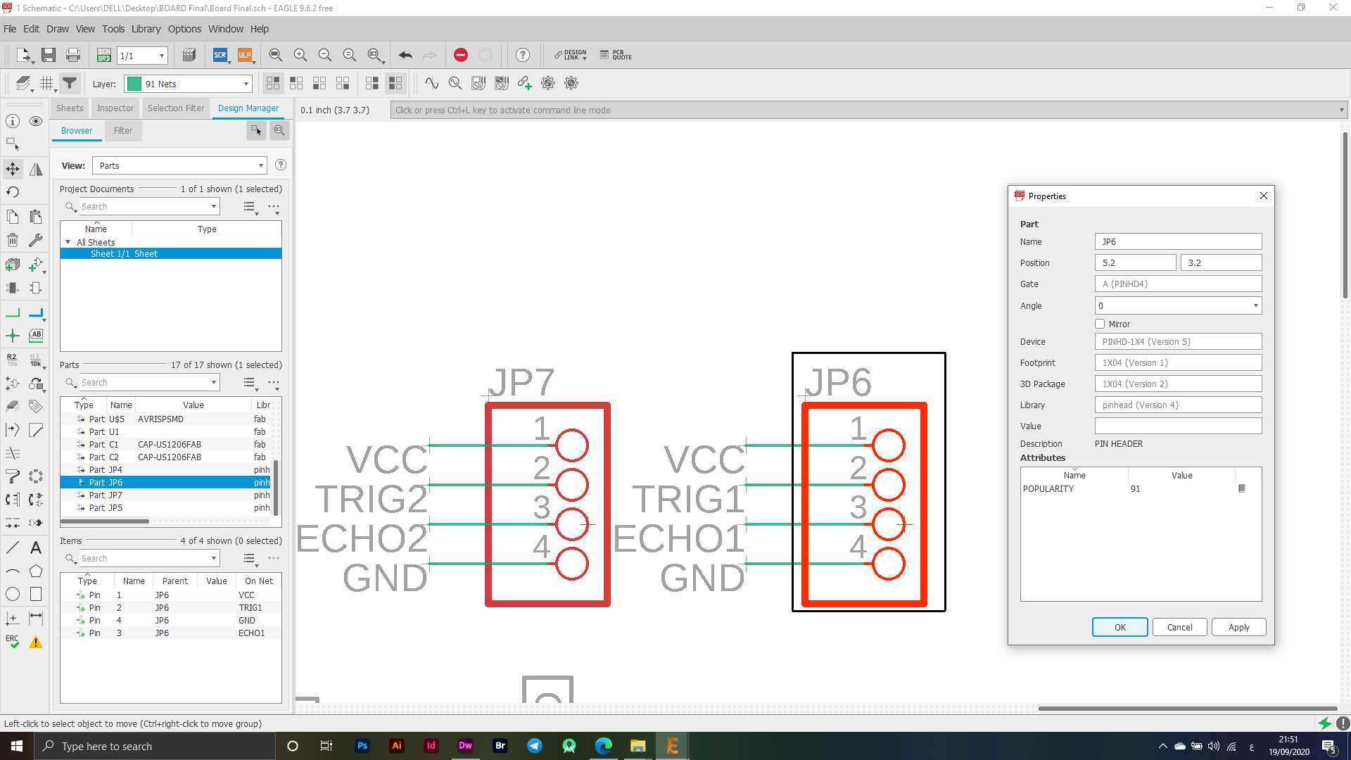
The image below shows my use of the PINS, I used them to connect the UlrtaSonic Sensor to these ports, and the following figure shows how the connection process will be and the names of the ports that will be connected to the Ultrasonic Sensor, which is the body-sensitive device that I will use in my project, as it will be one of the main elements that I will adopt It is also included in the project.
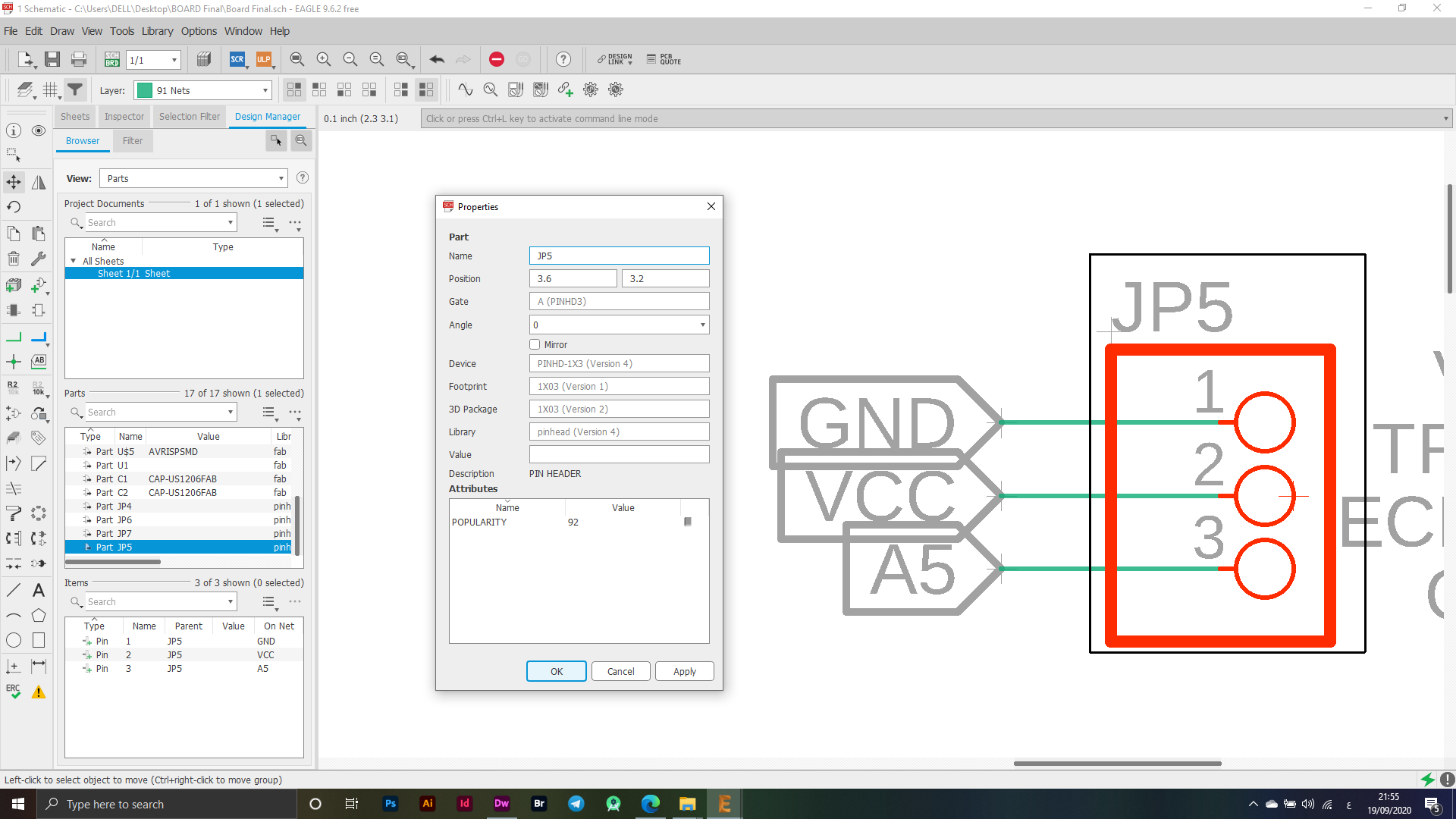
In this part, I will also use the PINS for the Servo Motor device, which I have set up its ports in order, as it will also be one of the most important elements that I will rely on in my project, which will move the device at certain angles to do the required operation of this project.
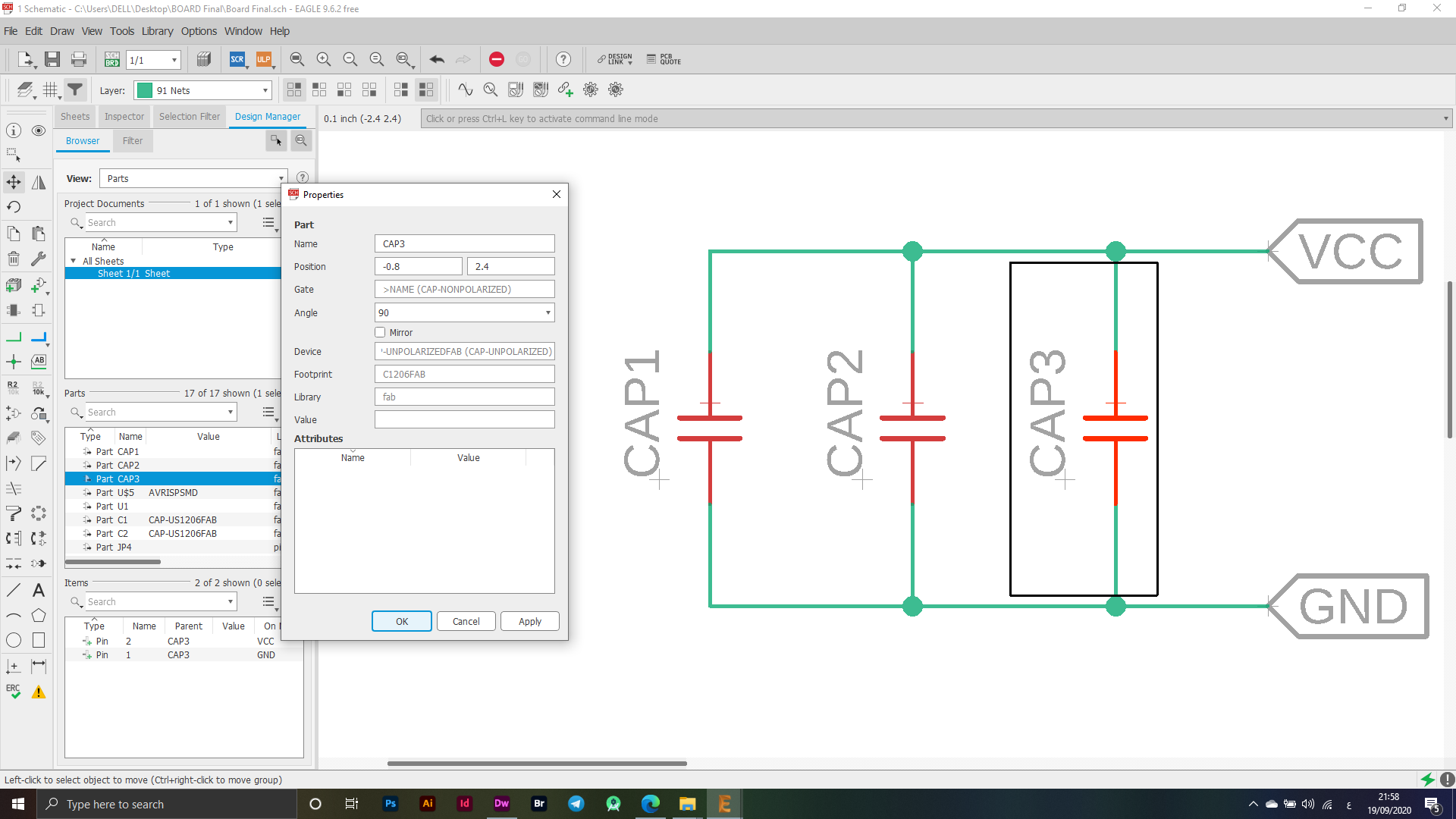
I have used a Capasitor to ensure that data transfer and operation are properly organized.
I used LED & SWITCH on the electronic board to test it when cutting the electronic board, to make sure that it was working properly and to make the operation more easier.
BRD - Board
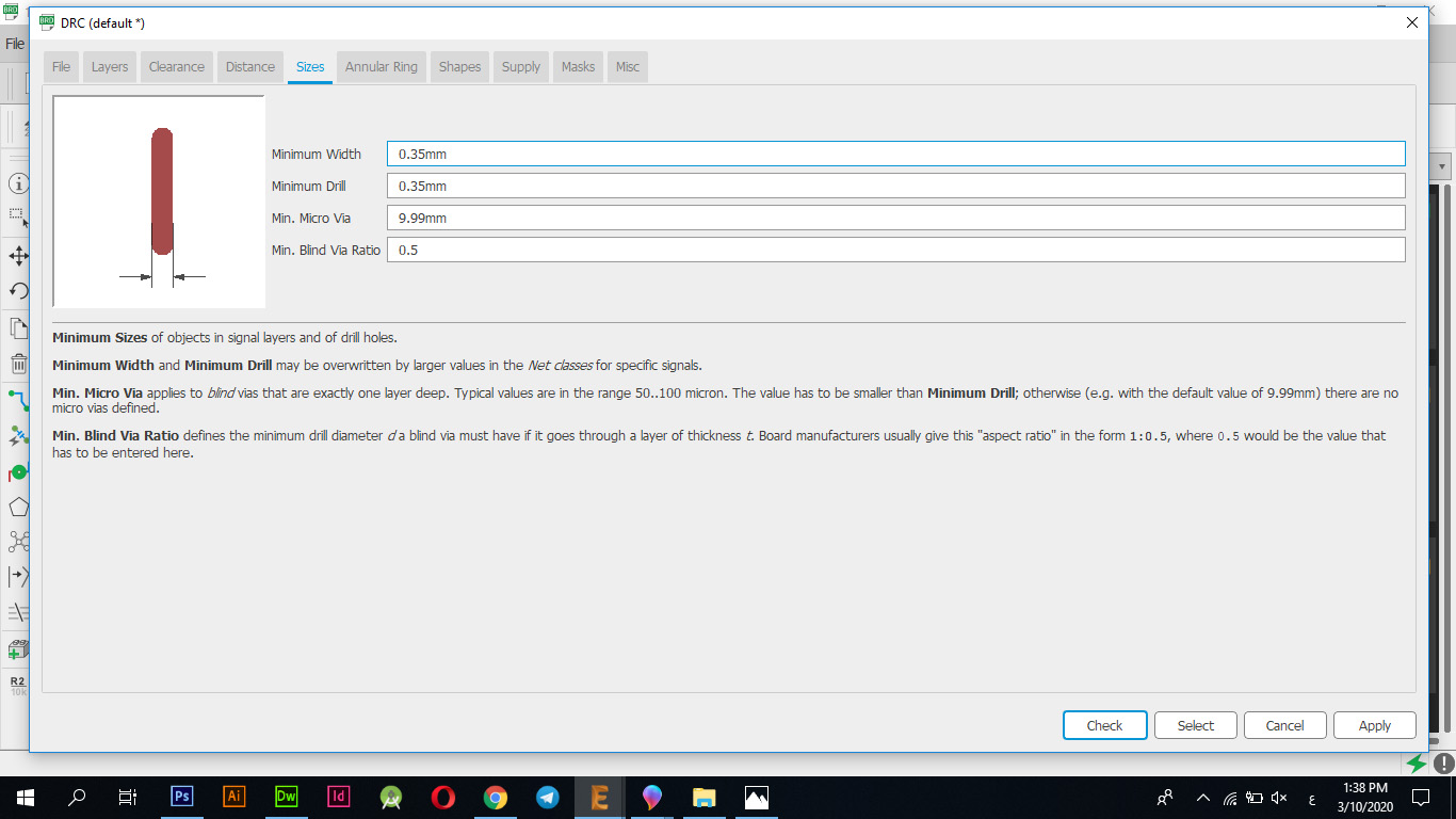
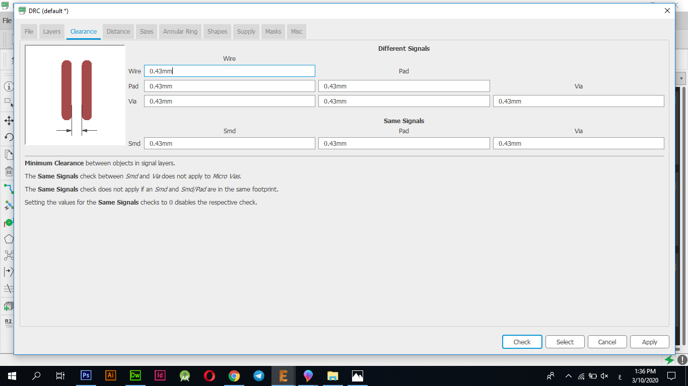
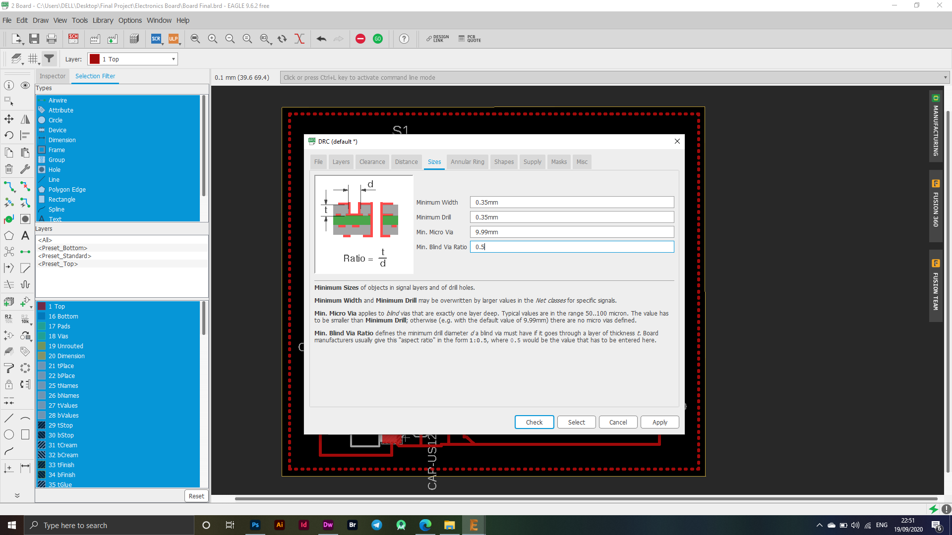
In the beginning, when I moved to the final stage of designing the electronic board, I set some settings from the Tool - DRC option, as these settings are the actual control over the thickness or height of the connections between the electronic parts, and the following pictures show the settings that I used in the process of connecting the board as it is Without adjusting these settings in advance, it can cause many problems, including unstable height or thickness of the connection between the electronic panels, which is what I was facing in the beginning of my use of Eagle.

I have made the connections based on many factors, taking into account that all the connections are correct, as I tracked each piece and where I will connect it with the other piece and thus formed an electronic board that I can use in my final project, as shown at the bottom on the left side a sign indicating Indicating that there is no error in this electronic board after verification by the program.
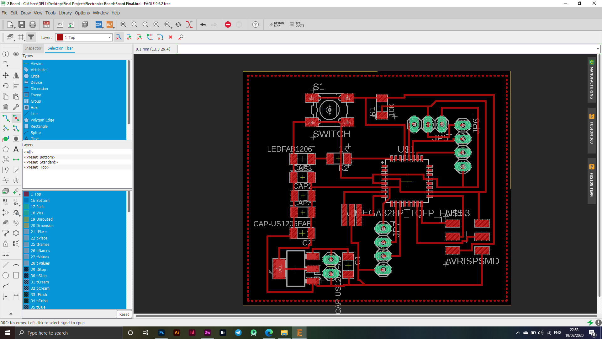
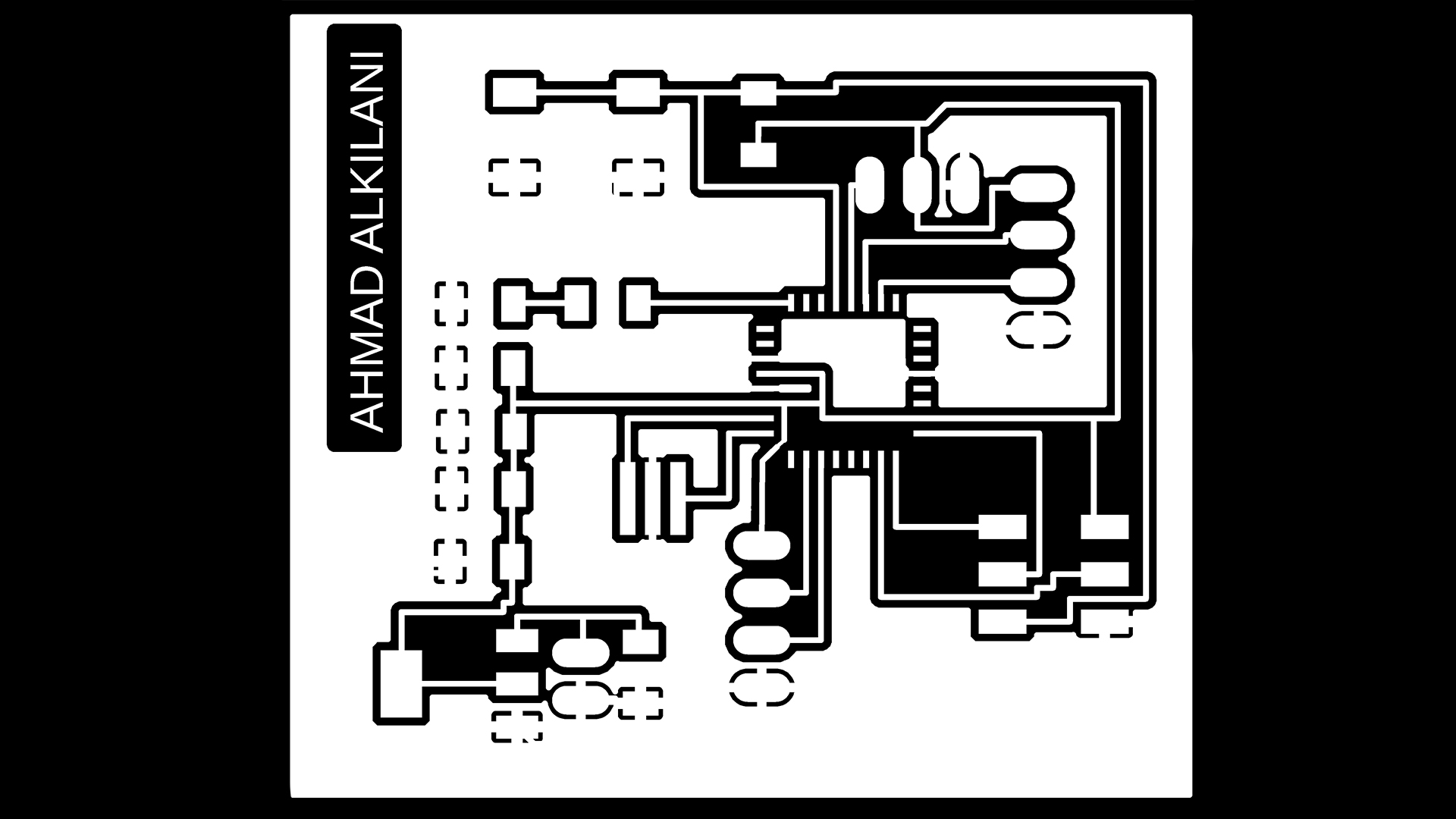
The picture below shows the final shape of my design.
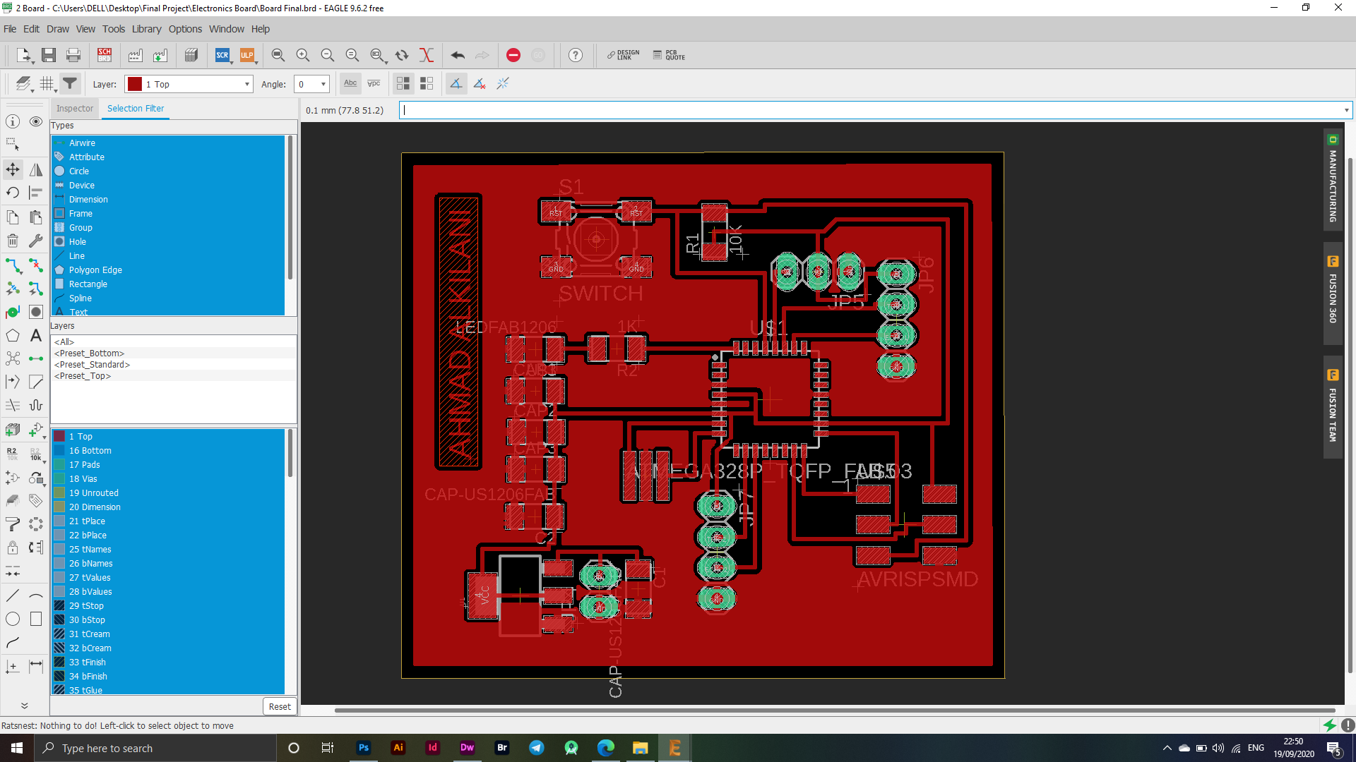
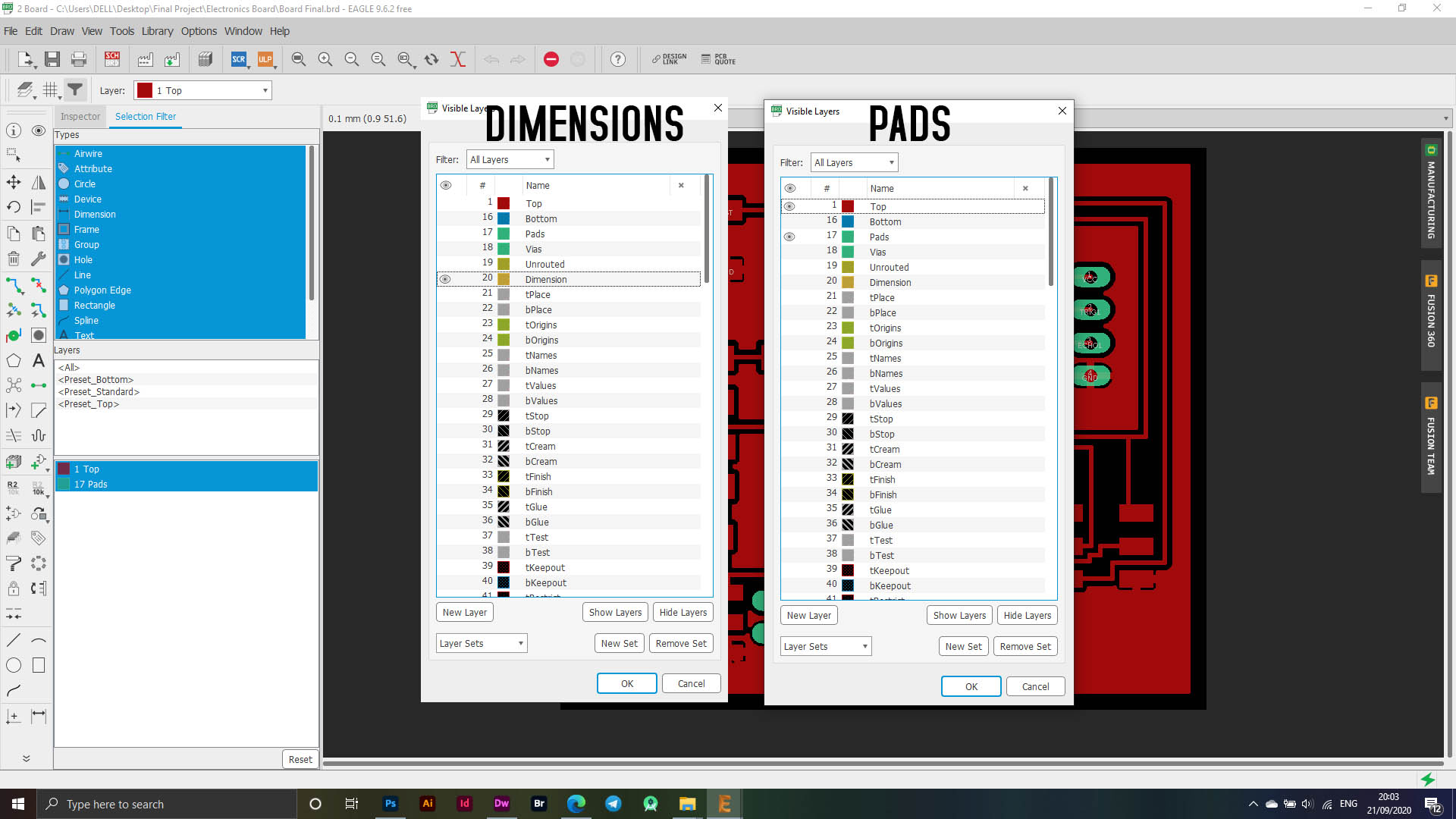
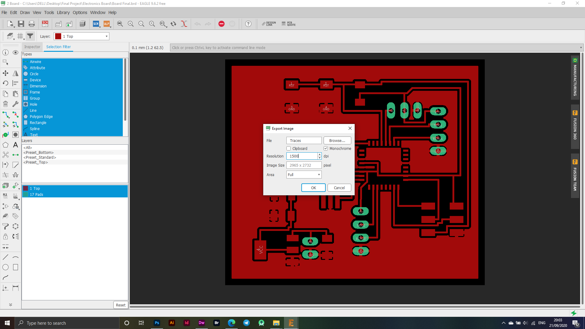
After hiding the layers and keeping some layers showing like Top - Pads, I exported my flap in PNG format using the File - Export - Image menu.
In the following picture, each window indicates the export process. In the first window, PADS, I exported the Traces by hiding all layers and showing the two layers "Pads - Top". In the second window, I exported the Outline by showing the dimensions layer only, and to export it with an image through "File -" Export - Image "The image below shows the settings and the selected dpi.
Fab Modules
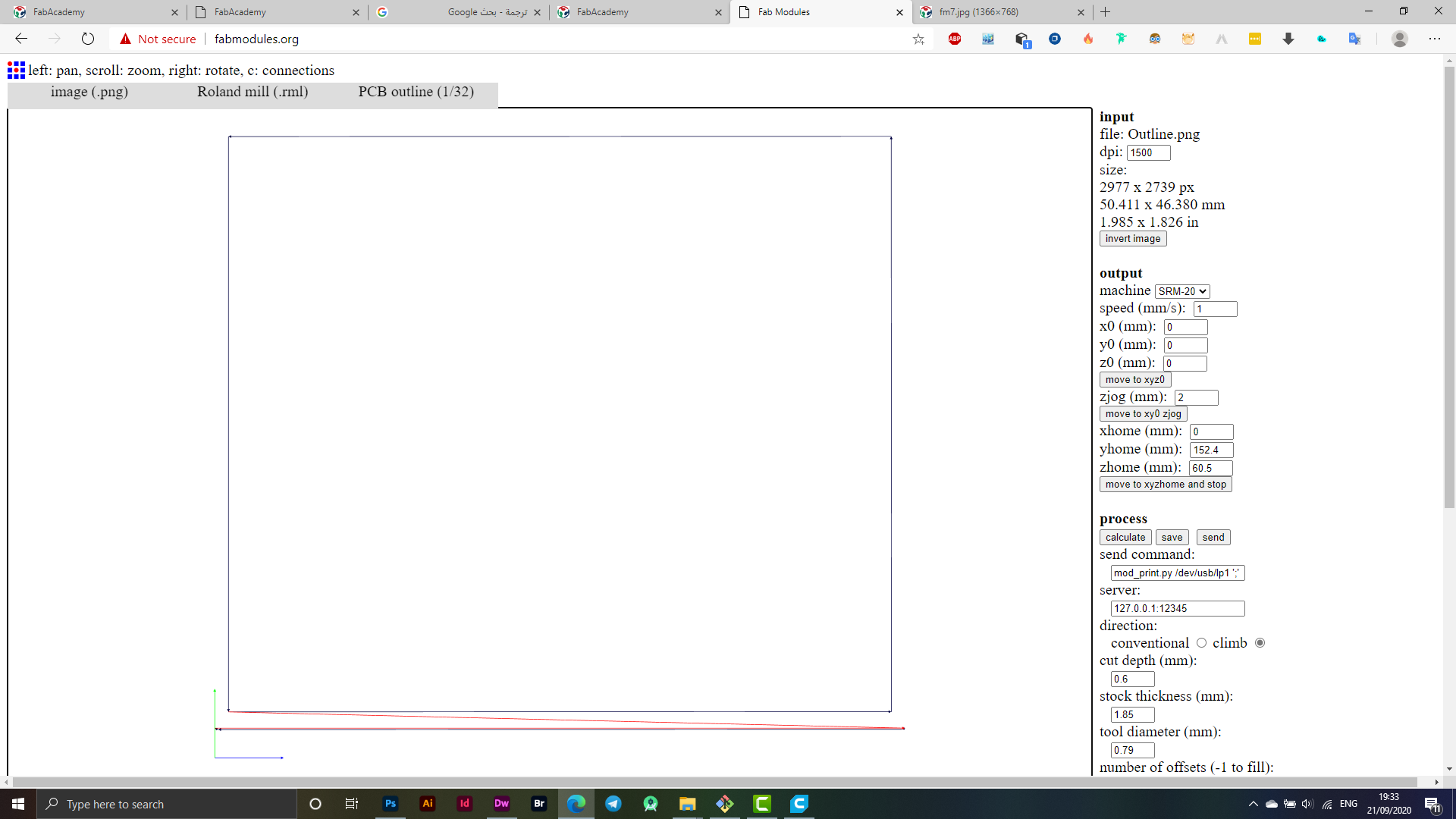
I logged into FabModules which is the site I usually work on to adjust settings while preparing the electronic cutting boards. Initially, I set the settings as shown in the image below:
Traces
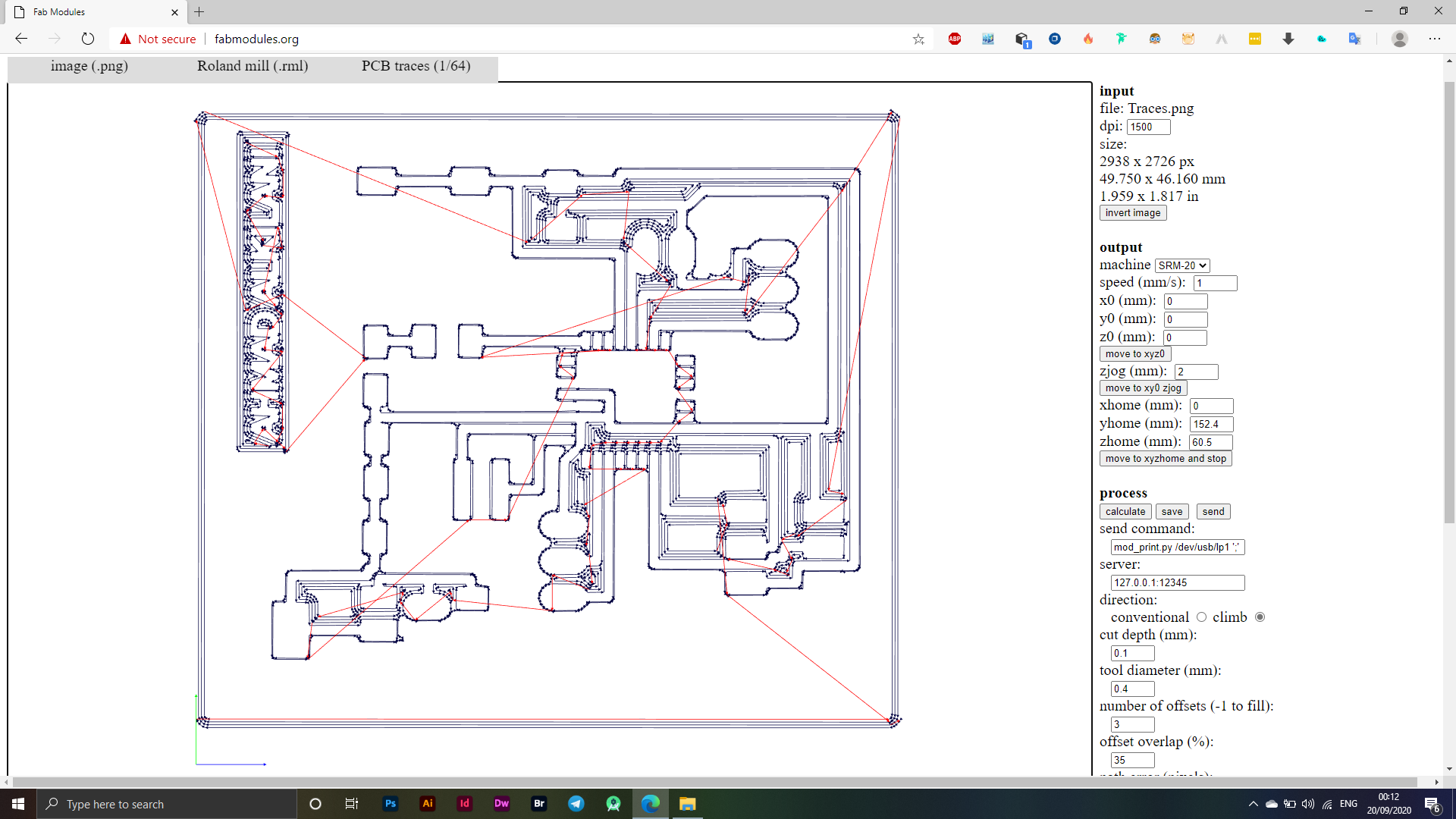
Outline
To prepare the files for cutting, I made a save for each file as it will be exported in (.rml) format.
Roland Machine - SRM20
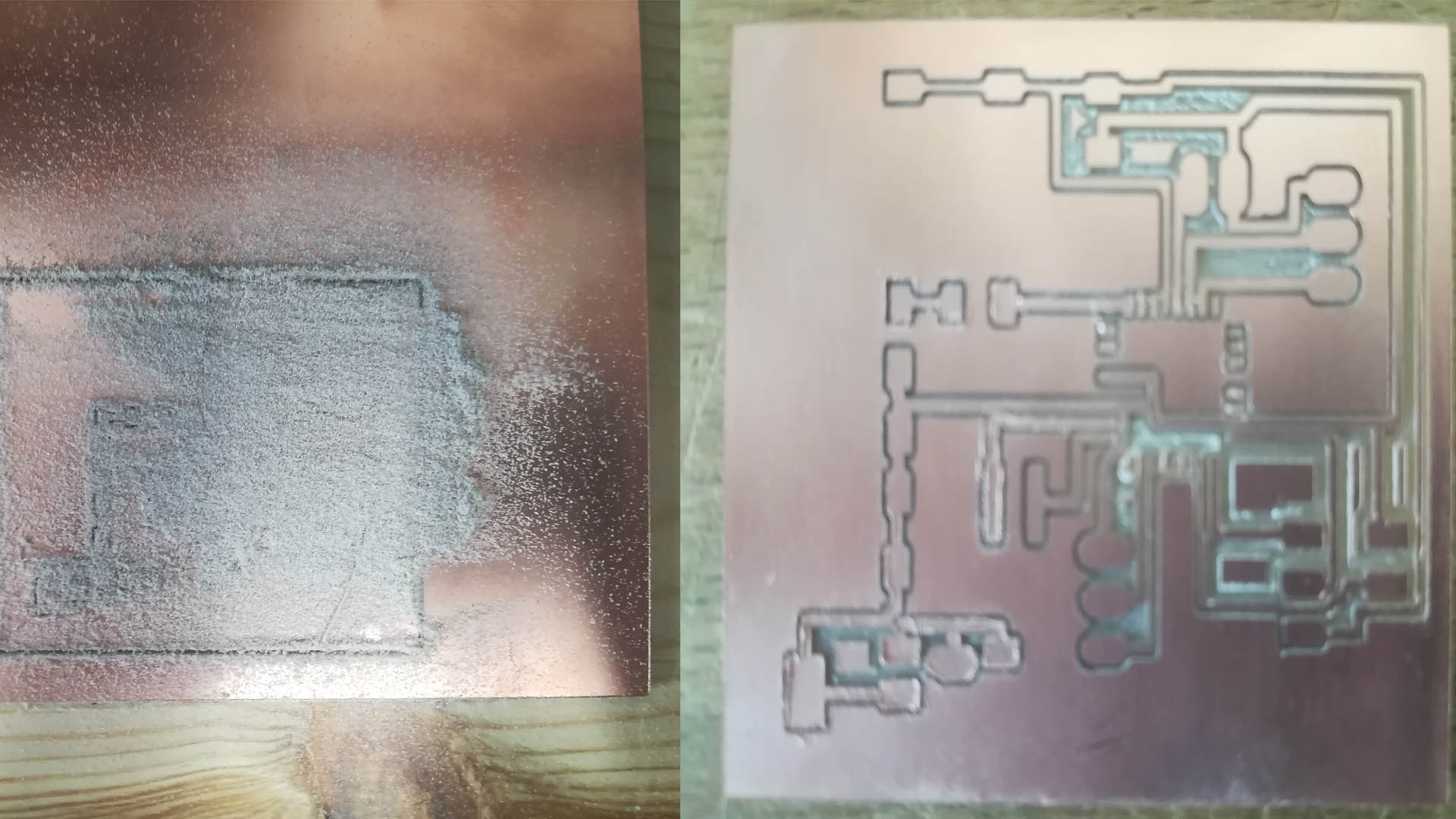
After exporting the files in RML format, I moved to the direct cutting process through the machine, where I zeroed the directions according to the electronic board available to me and in whatever location it was placed, the angle X, Y was zeroed according to the position of the electronic board while the one Z was reset based on making sure that he was able On reaching the board, that is, when doing a test to see whether or not it is connected through a voltmeter, the voltmeter must signal that the poles are connected to each other so that we can make sure that the operation will go well.
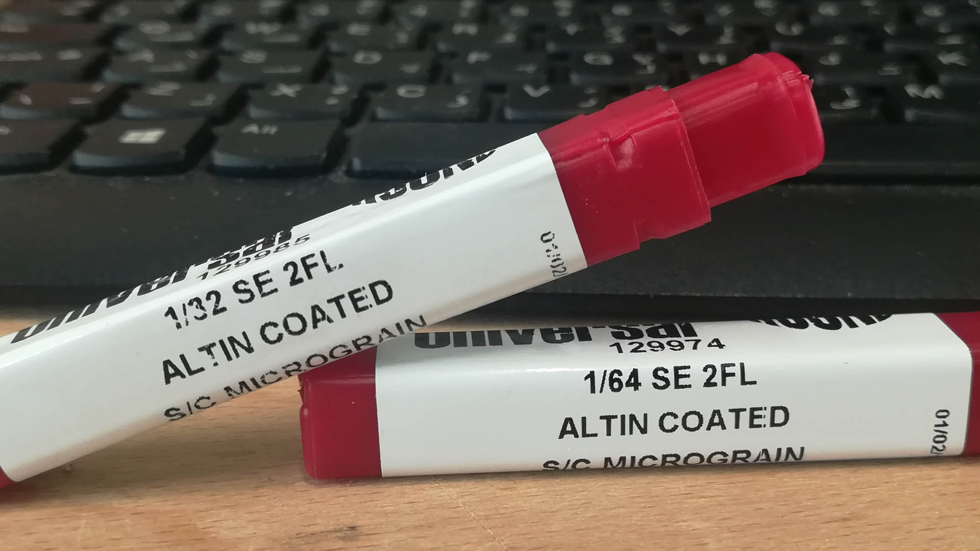
I used an End Mill 1/64 bit for my Traces cut, I used End Mill 1/32 for an Outline cut, the following image shows more information.
The image below is the final look of your design.
Soldering
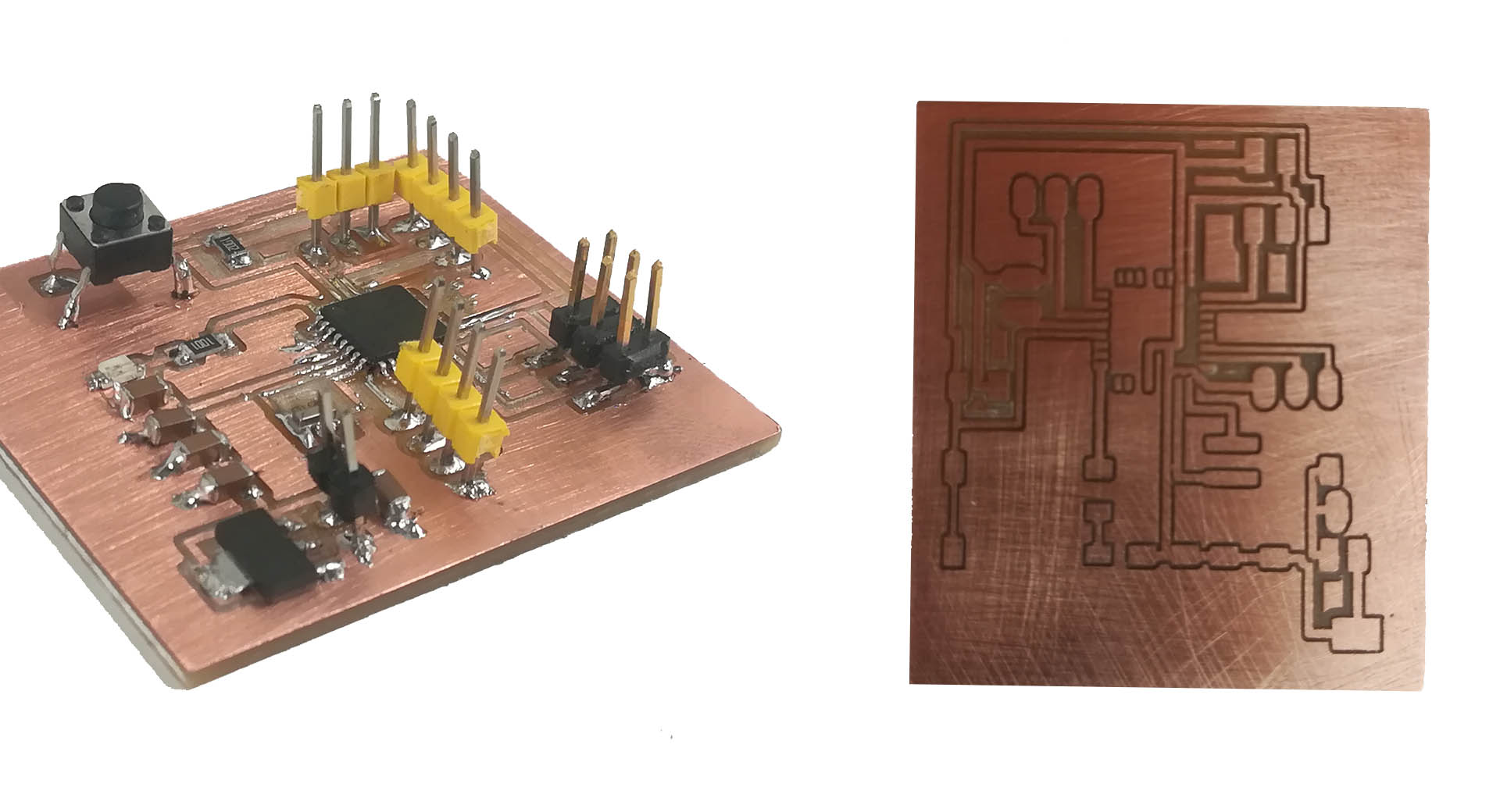
I welded the parts and as the picture below shows the welding process, the process of welding the parts took about an hour, in addition to that I encountered a problem during the process of programming the electronic board as I performed a wrong operation when welding the Resonator piece, which led to two ports contacting each other, and after making sure that it is the place Faulty I took apart the piece and re-soldered again, it was a really fun process.
Going to the programming phase and making sure that the electronic board that I designed is working, I used the Arduino IDE software.
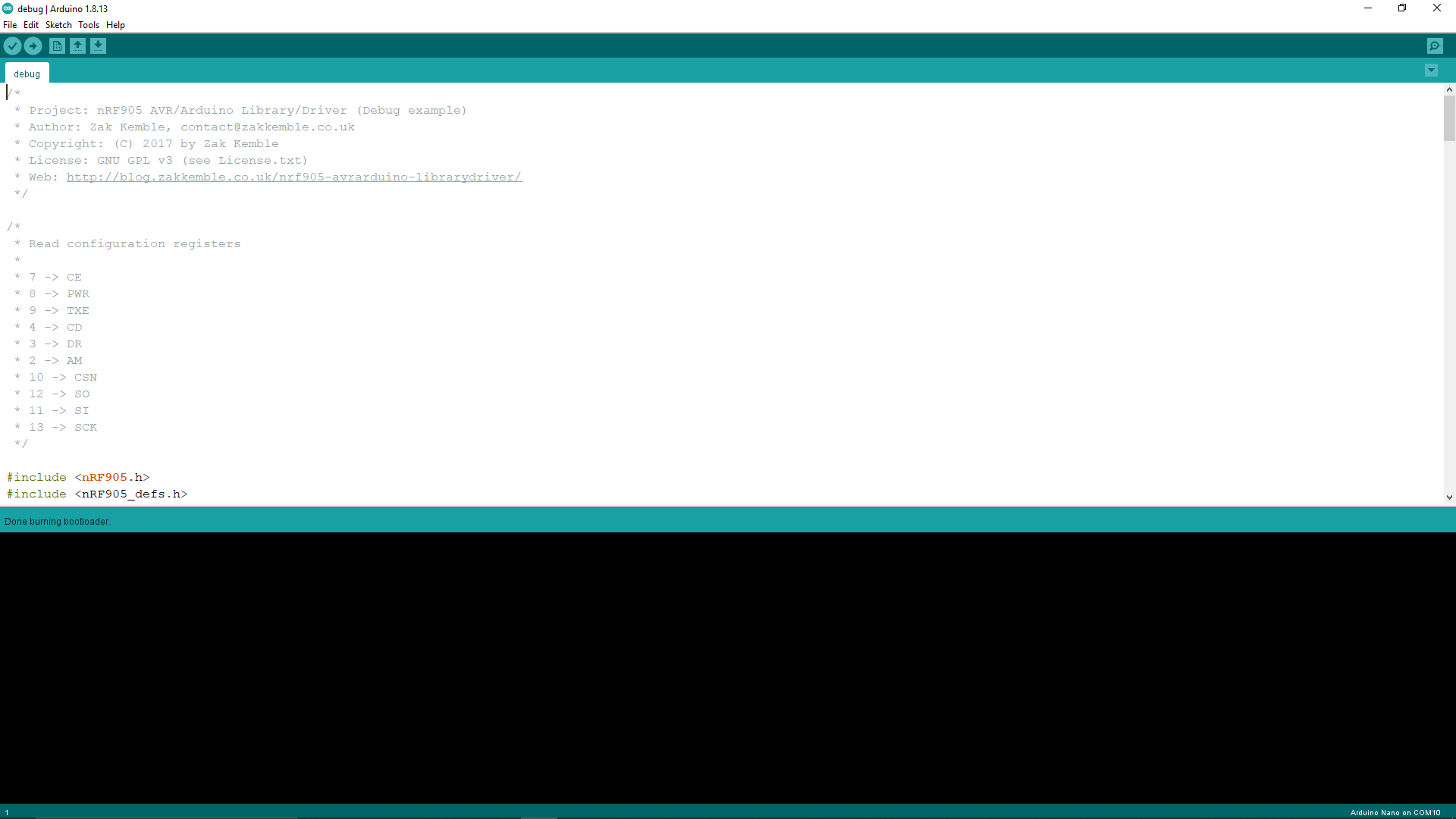
The image above shows the success of the operation as required "Done burning bootloader".
The following video shows the operation and testing of the electronic board.
Files - Open Source
Shematic & BoardGroup Assignment