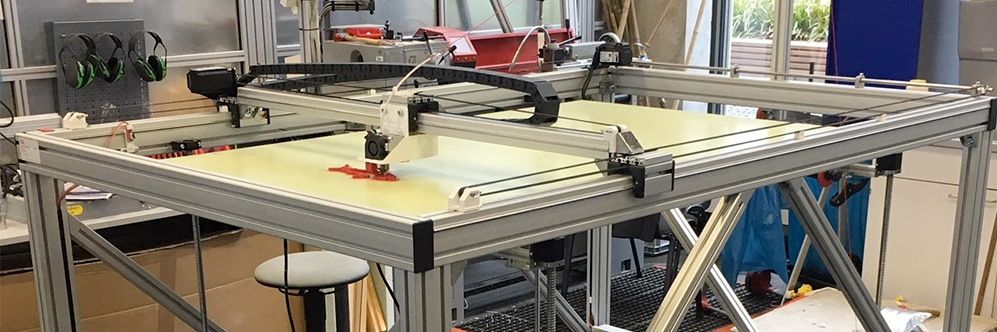
Big 3D-Printer
With a maximum volume of 150 x 90 x80 cm
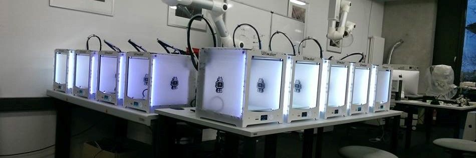
Some of our Ultimaker
We´ve got more than 25 3D-Printer of diffrent types
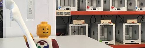
Greeting
Our best employee in HRW FabLab
Assignment 4:
electronics production
Task:
- characterize the specifications of your PCB production process (group project)
- make an in-circuit programmer by milling the PCB, then optionally trying other processes
Work
Welcome at the first real electrotechnical assignment. With my background in mechnaical engineering i have got only quite rudimental knowledges in electronic design so this type of assignment will getting harder for me than ne mechanical production. That’s the reason why I didn´t use the electronic corner in our lab (see below) for more than small soldering fixes. So let´s take a closer look to our maschines: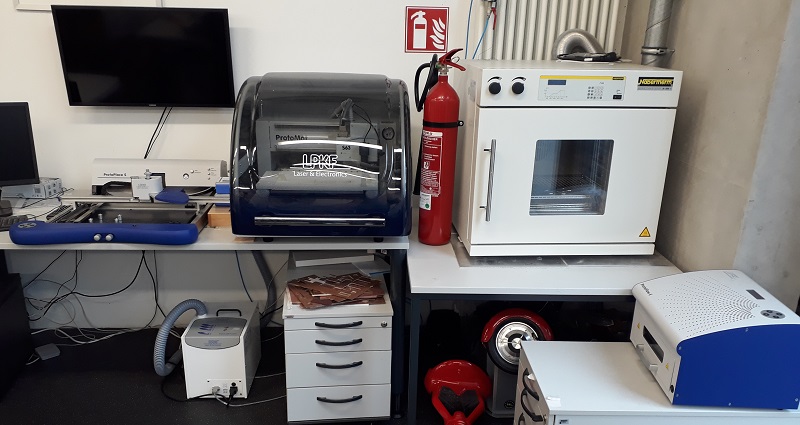
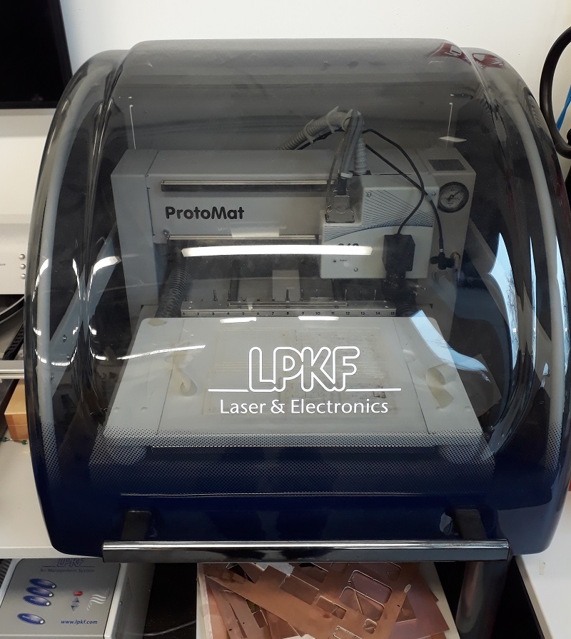
The LPKF is our milling machine for our electronic boards. This machine has a lot of additional functions like a onboard camera but in the past we have got a lot of problems with broken parts. So at the moment the LPKF only works in their basic mode and you often need more than one try before the machine works well.
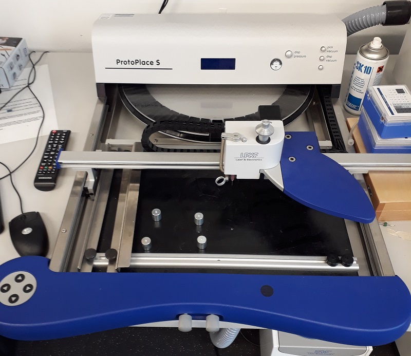
The nest machine is for assembling the milled board. It allows two working steps. First you can place small drops of solder at the necessary areas of the board. It is quite precise. The nest step is to handle the small electronic components and place them on the right spot. In the best option you do this without building bridges between the single conductors.
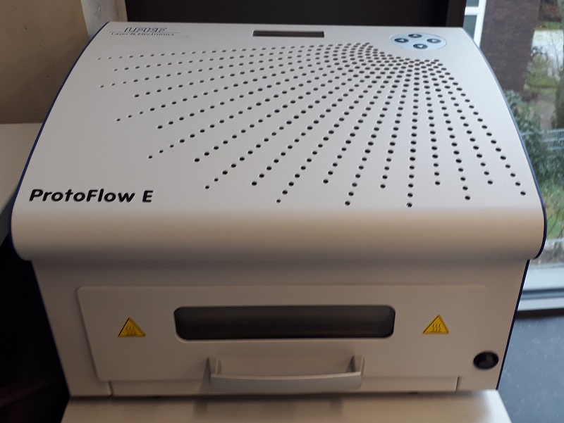
The last step is the oven. Here the solder builds a strong connection between the electronic components and the board. It is quite simple to use and works like your oven at home. Only the temperature could be regulated more precise. The single bake process is always the same. First the oven gets a minimum temperature, then you insert your board and the oven holds the temperature to preheat the board. After this stage the oven raises the temperature as quick as possible to melt the solder but not to destroy the single components. The time this complete process needs depends on the size of the board and the used components. As bigger the board an the components as longer are the single heating phases.
But before starting with the production process, lets start with the layout.
I used Eagle 8.6.2 for my board development. For students and scientific research assistants is this software for free. It uses the same login dates like Fusion 360, cause it is also a Autodesk tool. I´ve never worked with eagle before so I had to install it first. The installation is quite simple, and there is no additional explanation necessary.
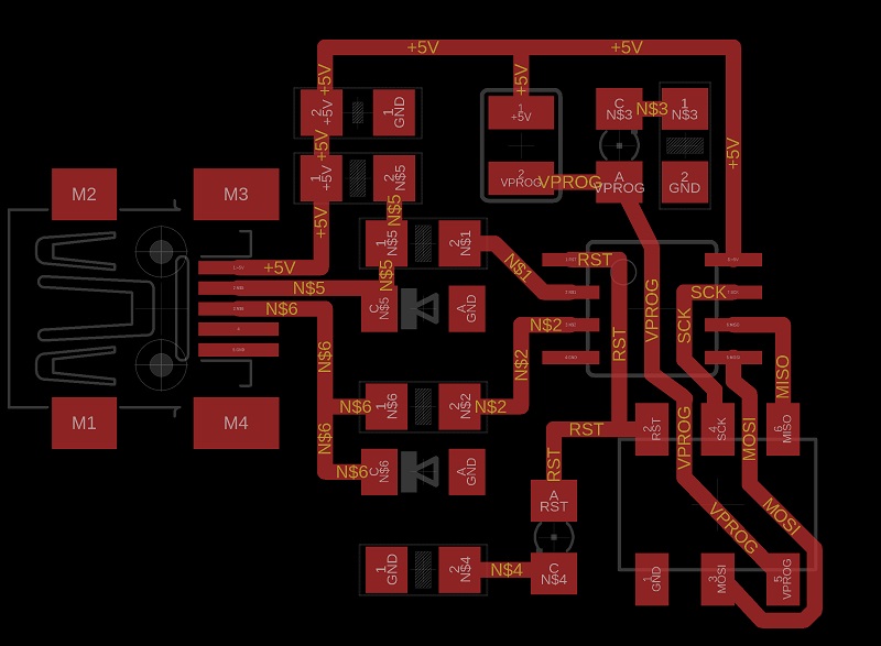
For the connection scheme I decided to use Brians model and develop my own layout on the board. The complete development of the connection scheme would be a too great challenge for me in just one week.
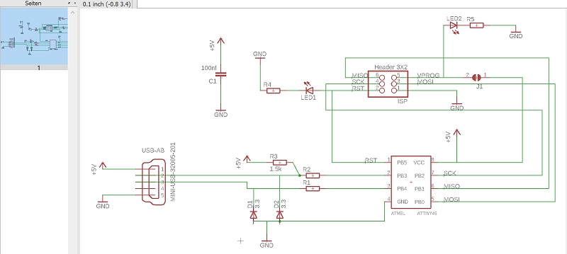
So I learn again the basics about electrotechnics to understand the connection scheme. In Eagle I started a new project and added Florians finished connection scheme. He changed some small parts in contrast to brian, because we didn´t have the same components in our lab. See the model I used below:
I used this model to generate my own board design. Therefore I changed to the board tool in Eagle. In the first step I made a quite rudimentary layout sketch and pulled the single components in different directions until they didn´t lay on each other anymore. The next quite useful step was to make the complete board GND (ground). Now a lot of connections between components disappeared. The next step is like a puzzle and I needed a lot of time to generate a functional layout. I started at the USB and followed the connections until I found a potential solution. In the next step I tried to found a more compact solution. At this point I didn´t mentioned that it is quite more easy to assemble a bigger board. See my final Layout below:
In the next step I checked the Design rules. Therefore I set the settings to the following values. The Values are the standart setting for eagle and they works quite well. Our milling machine is able to work with smaller distances but this makes smaller tools necessary which are more expensive. See here the possible tools our machine uses:
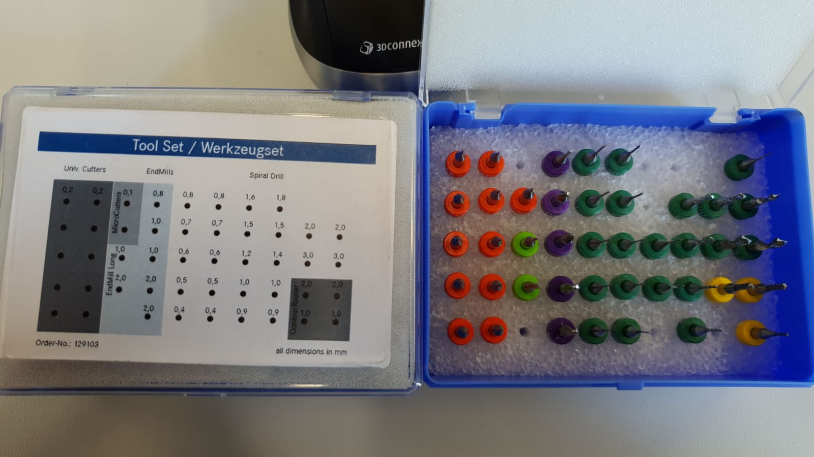
As you see there are milling tools down to 0.1mm diameter but the standart tools are the 0.2mm which relate to the 8mil you found in the settings below. Also with the 1206 parts is is not necessary to mill smaller contour. Our LPKF milling machine calculate ne needed tools by itselfe and show if there is a tool-change necessary.
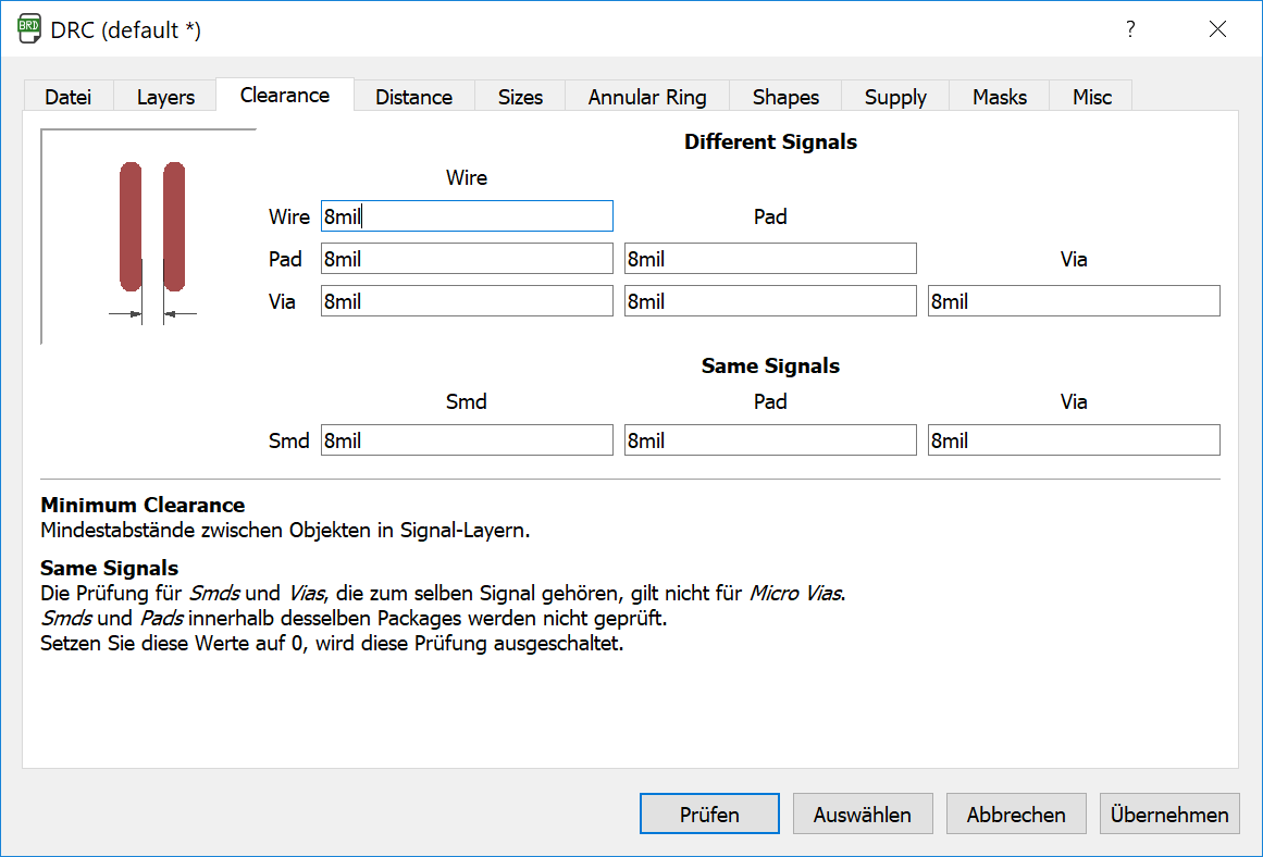
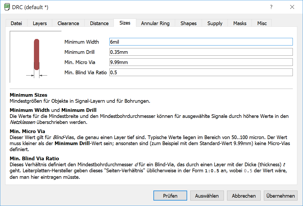
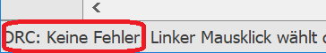
Also the postprocess is quite more difficult, because you will build faulty bridges more easy. After checking the DRC there are no more mistakes:
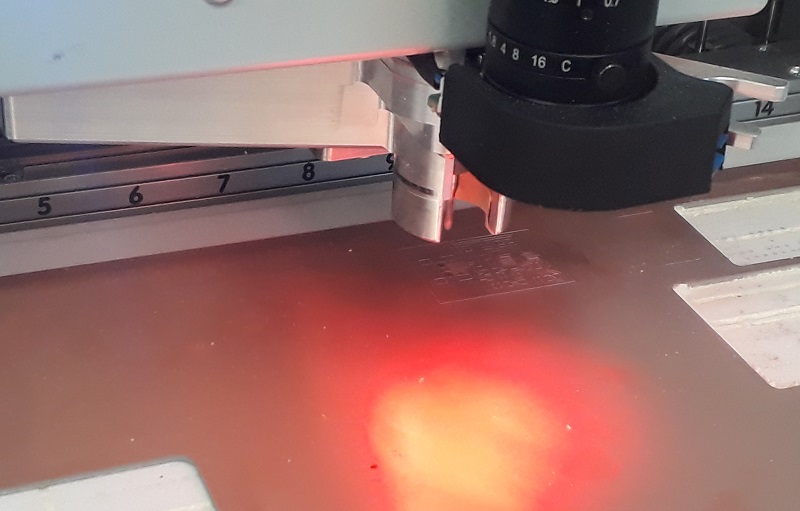
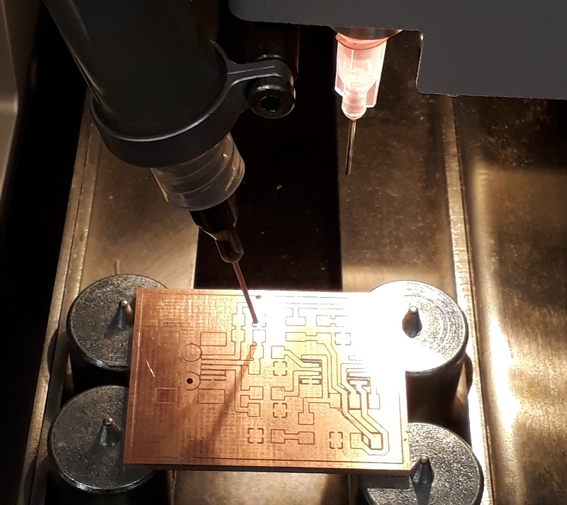
With this layout we can now change to the production part. Find the detailed production part documentation in our Groupsite . The Layout hat to convert into a CAM-process. This needs a few steps and some special justifications to get a useful board. At this point Tobias was a great help, because of the broken parts of our milling machine (we are waiting for it since month) I had to act with caution. He helped me to control the process and prevent more damage on our machine. See the mashie during work process below (the red light is for the camera).
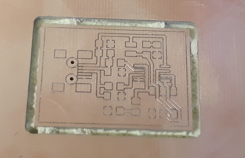
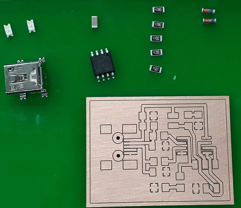
See below my first self-made board. After a short checking under our microscope I found some possible bridges in the board. But with a sharp knife I could fix it. So the next step is the addition of the electronic components. In the picture is the jumper and the header missing. I had to organize them before I started the finishing.
In the next picture you can see the tools for the assembling of the components. First I used the left needle to put the right quantity of solder on the single footprints. In the next step I used the right needle to handle the components and put them on the right place. This needle works with vacuum.
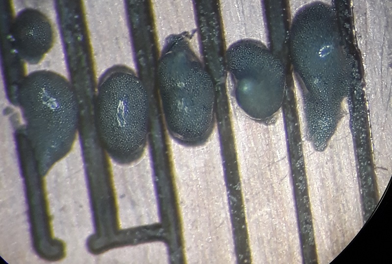
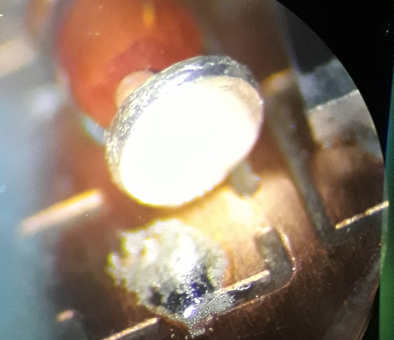
Here a picture of the solder on the board through our microscope. You see single solder balls in a liquid. Afer soldering it will become a homogeneous connection.
Below you can see the process. First during the placement of the components and then after a short trip through our oven. I used the adjustment for big boards, because with the USB connection I used a massive component witch needs a lot of heat. At the first look I think it looks great.
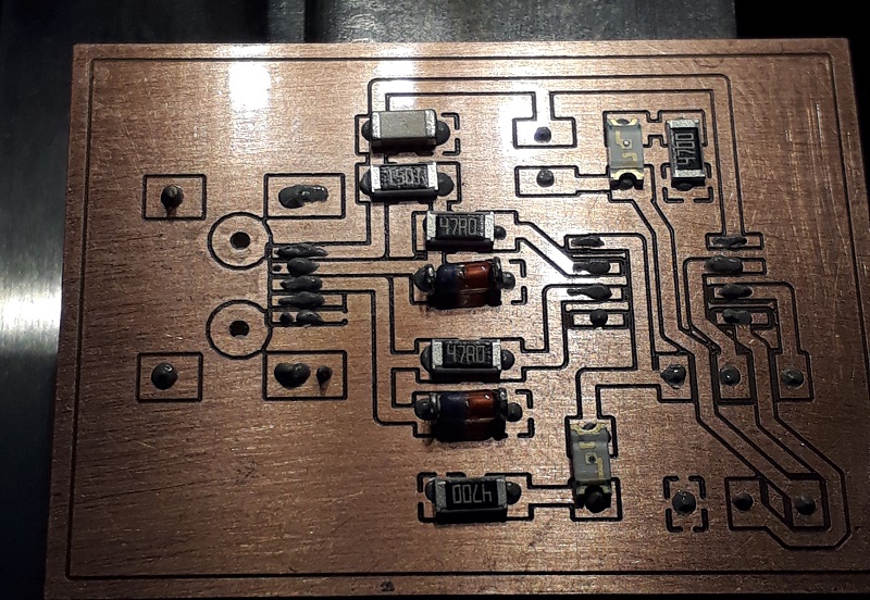
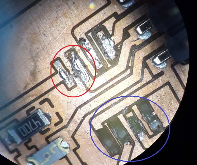
But then I had to check the board. And I found some failures quickly. First as you see one of my diodes rolled out of the soldering so is wasn´t connected to the board on this end (see red circle). I had to fix it by hand with a small addition of soldering. The rest looks nice, but during the connection checking with our multimeter I found a connection between the ground and one of the AtTiny 45 foots. I can´t see se mistake so I had to remove the complete AtTiny. That caused a big damage of my board, because I didn´t remove the solder but some complete parts of the electric conductors gets broken. So I had to fix them creative
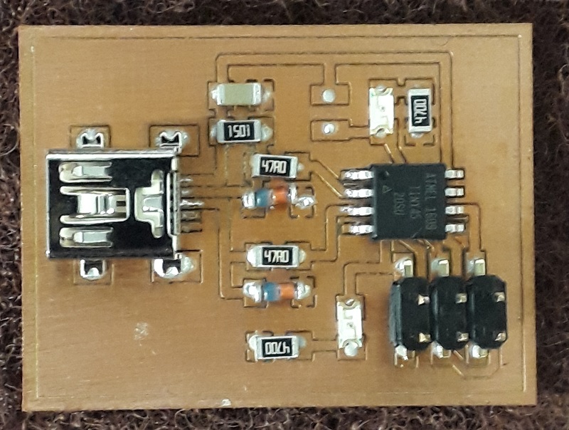
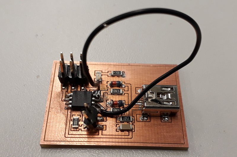
So see here my final programmer. As you see I added some super cool special gimmicks like the absolutely useful handle out of strong cable. Ok, I didn´t find another chance to get the right connection of the broken AtTiny footprint. But this connection works well and after this quick and professional fix there are no more failures in my board.
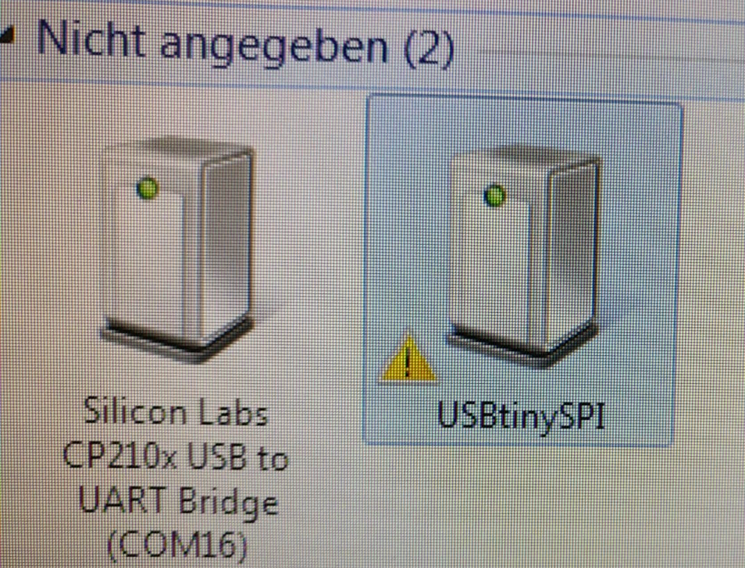
So finally I had to check if my designer board works. But with my windows pc I had some trouble with the installation of the software for the building and programming of the firmware onto my board. Soe of Brians Links didn´t worked anymore and my search after other sources wasn´t quite helpful. So I decided to check my board on one of our iMacs we´ve got in our lab. Here the process worked quite well, but take a look on your own:
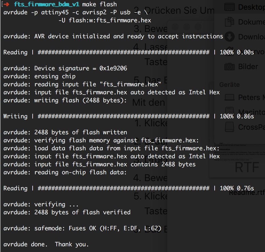
Finaly my programmer is noticed. There are troubles noticed by the iMac but the programmer works.
Downloads
| Eagle_project | download |
