Electronic Design
Tachometer
For the electronics of this project I basically wanted to make a tachometer (revolution-counter, tach, rev-counter, RPM gauge) which measures the rotation speed of my turbine. The device will display the revolutions per minute (RPM) onto an LCD screen.
Hall sensor
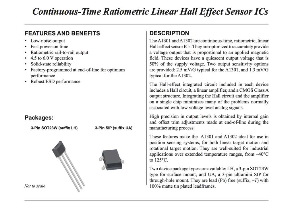
Testing this idea The tachometer is an spinoff from my input week where I used the Hall sensor to measure a magnetic field. The idea is to place a small neo-magnet on my axis shaft which would be detected by the sensor and then write a program which will count the number of rotations. Here are the A1302 Hall sensor specs:
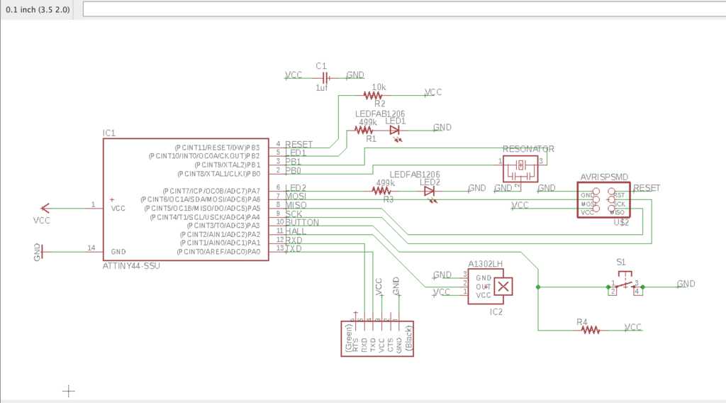
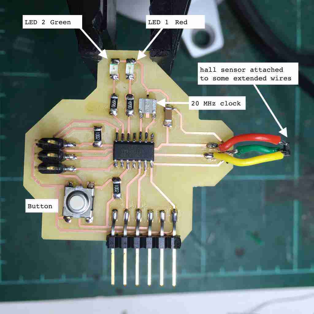
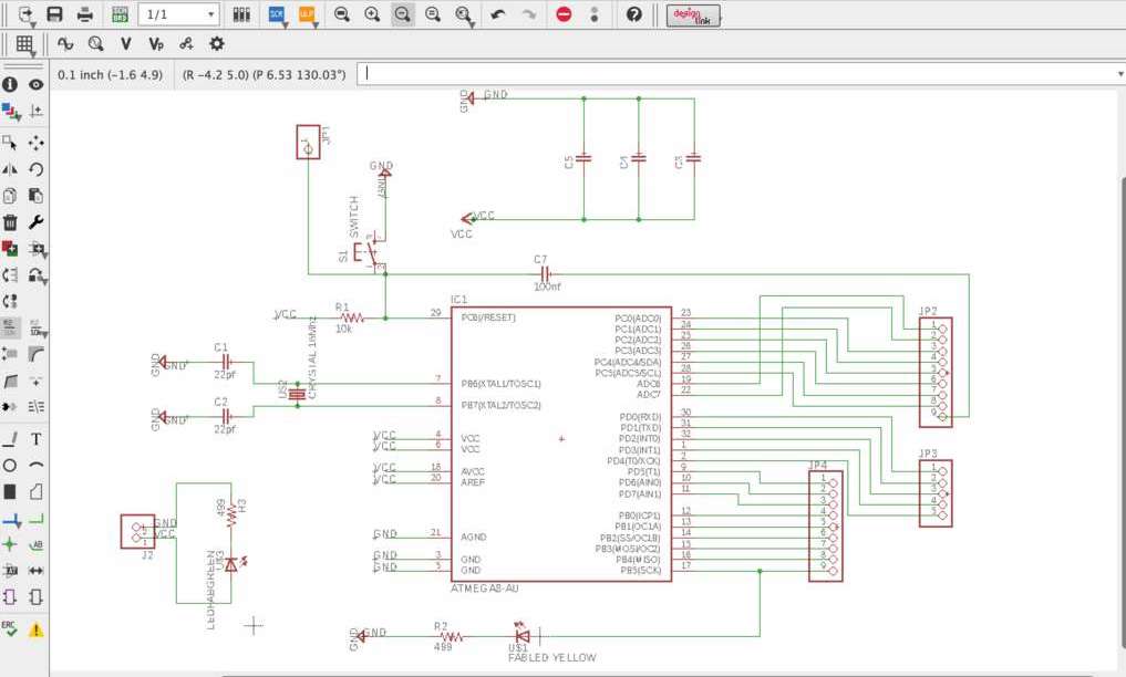
Here are my PCB designs in Eagle. Specific to this tachometer are a 20 Mhz resonator because i figured the timing needs to be very accurate. I also added two LED’s. The first (green) I wanted to indicate/blink on each rotation, and the second (red) I was thinking could indicate as certain threshold (like to indicate when the turbine is rotating below a critical rpm) so as to warn when there is a lower generator/voltage so drawing disproportionately from the batteries/capacitors.
 |
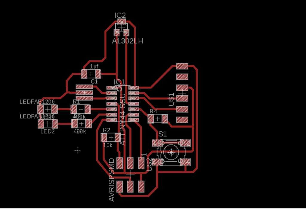 |
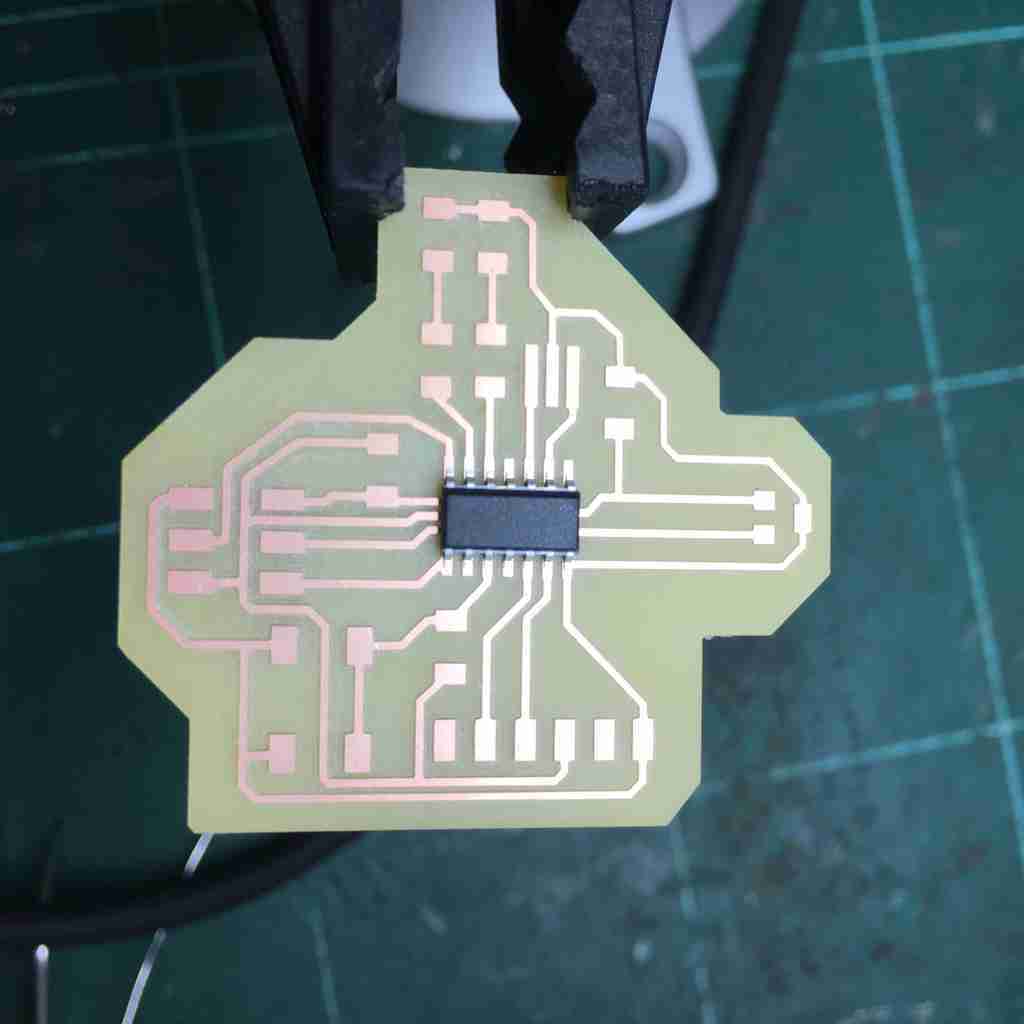
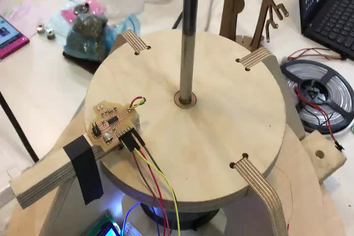
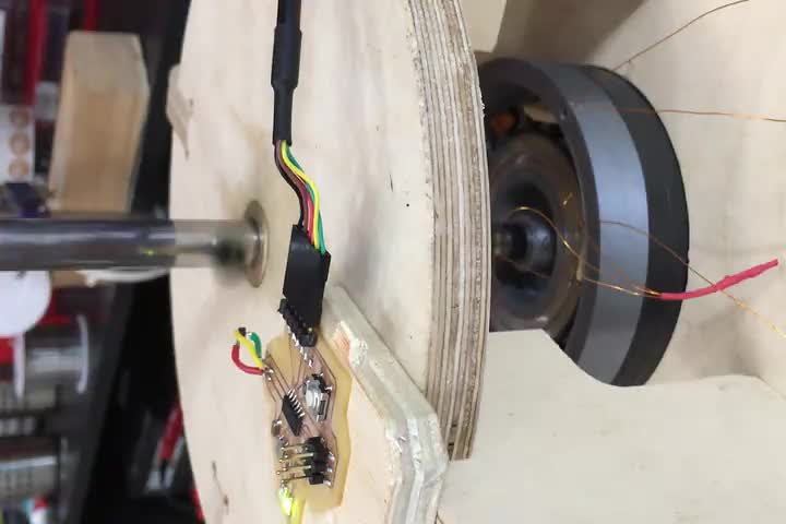
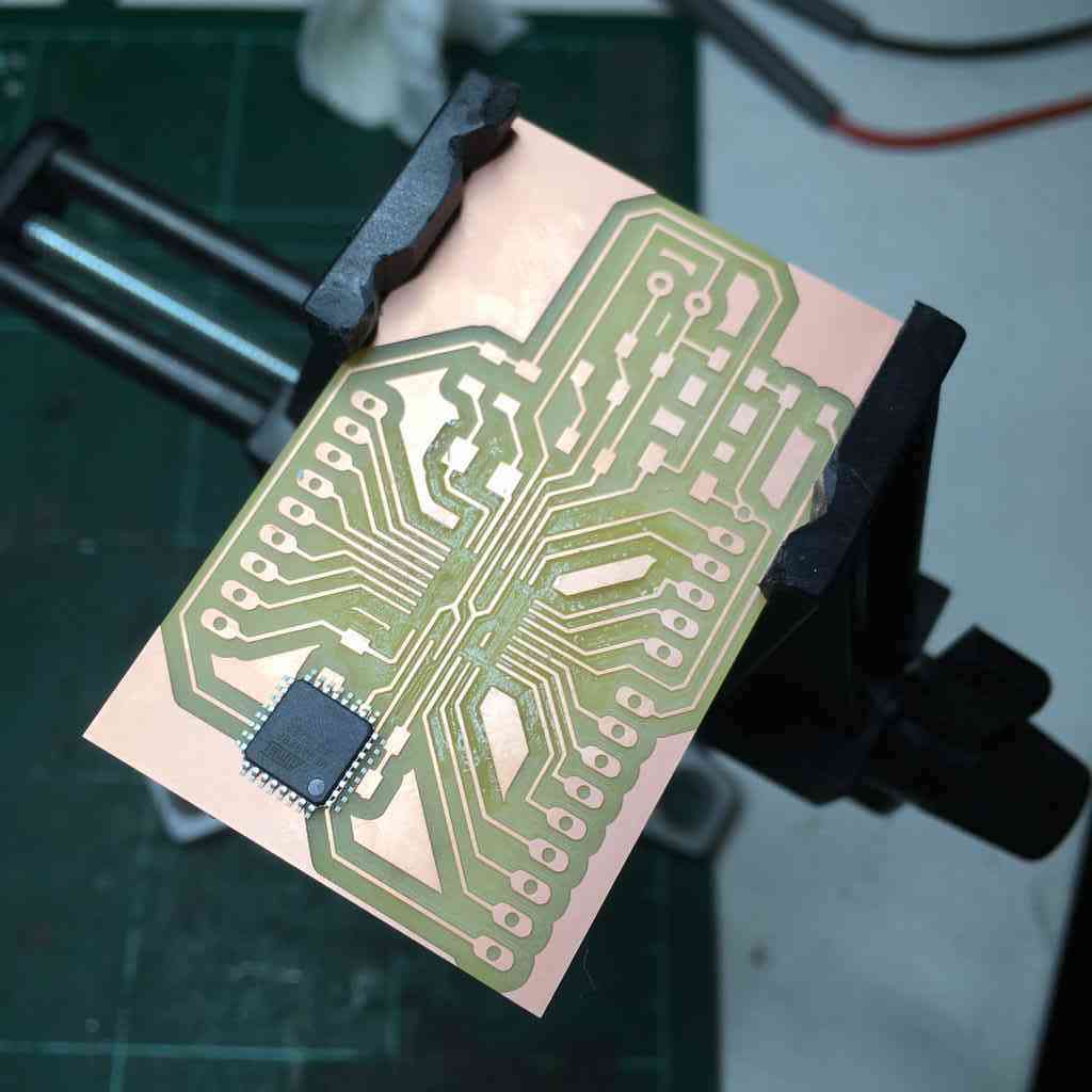
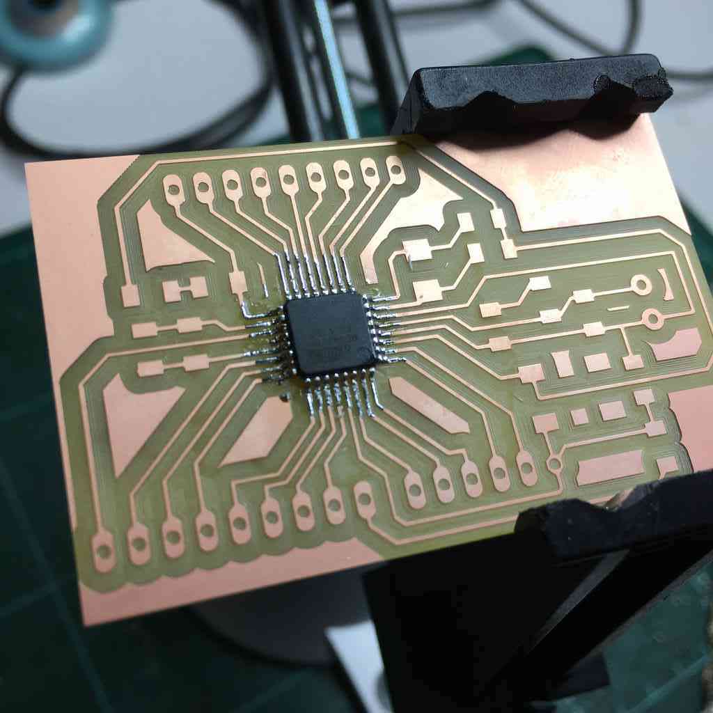
I also added a button to Pin 10 with the idea that if I wanted i could press it to turn the LED’s off to conserve power. Here is the PCB, milled and soldered. As you will notice I extended the reach of the tiny hall sensor because I wanted it to get as close to the axis as possible.
 |
 |
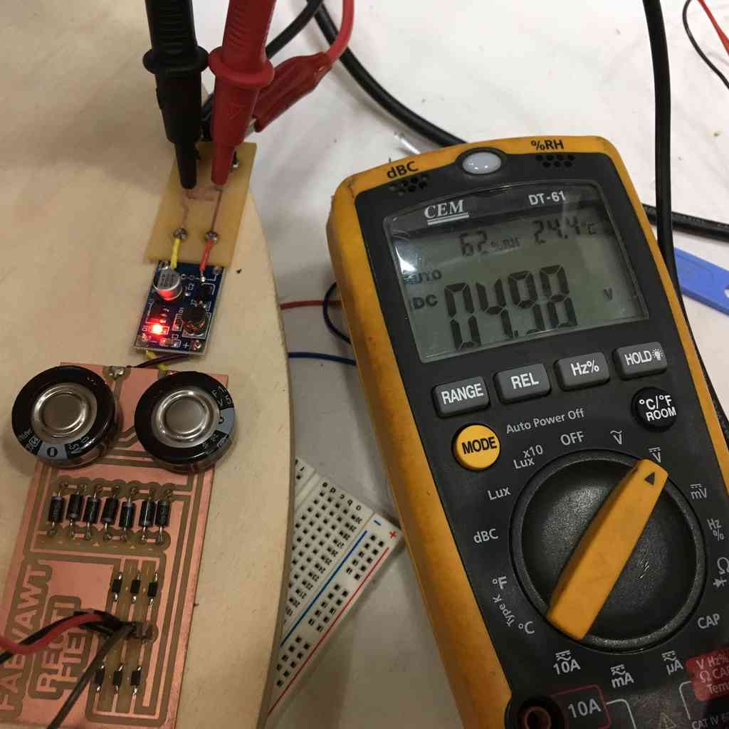
Here ere I am testing my tachometer, using an Arduino attached to an LCD display to read the serial output.
And here is my tachometer working with while I was testing my generator, and I am reading the RPM and Hz readings directly in the serial monitor.
You can download my Eagle PCB files here.
Rectifier + Charge Controller
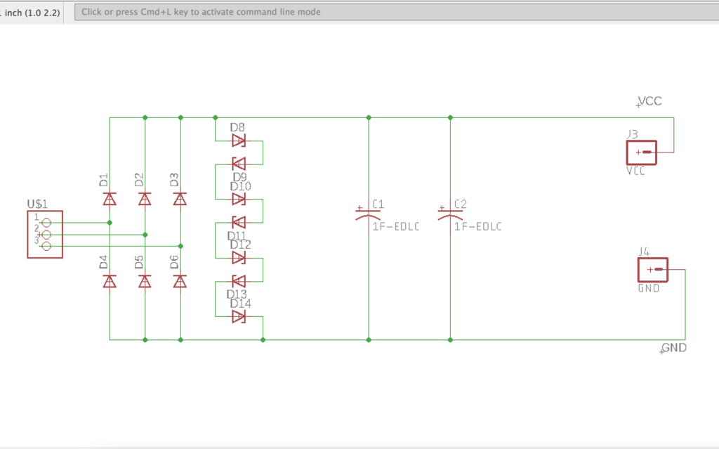
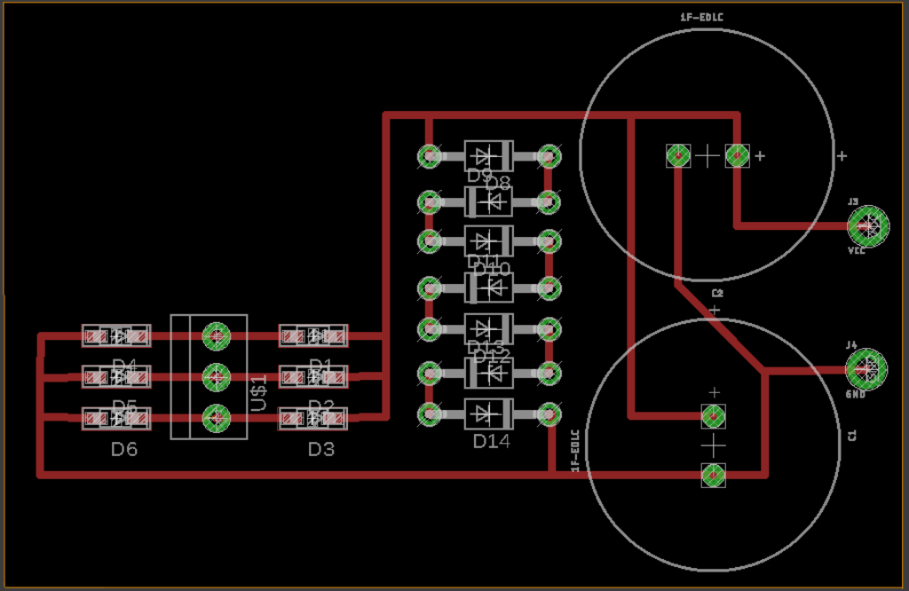
Now that I had the rectifier working on my breadboard (see generator), I went ahead and designed the electronics in Eagle using the components we had available in the lab. For the 3 rectifying diodes, I used the Shottky SMD components as they are supposed to have a lower voltage drop that regular diodes. For the dump load I used regular diodes.
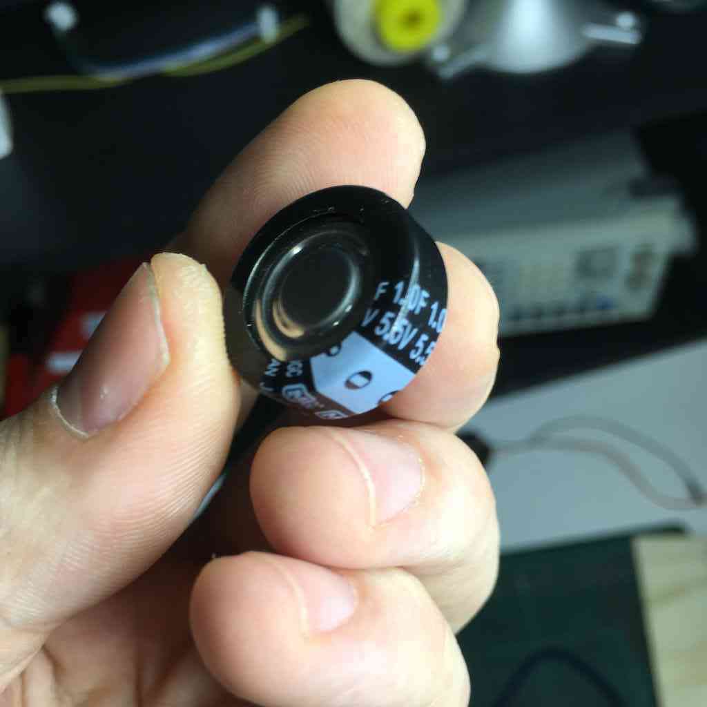
As for the supercaps, the the time being I am using 2x 1Farad (5.5V) capacitors connected in parallel, simply because I could not fit more onto the PCB board for the time being.
 |
 |
And here are my supercaps:
Because I was going to connect the PFM module. With an input voltage of 0.9V to 5V DC, the module gives a stable 5V DC output through its USB socket.
Pulse-Frequency Modulation (PFM) is a modulation method for representing an analog signal using only two levels (1 and 0). It is analogous to Pulse-Width Modulation (PWM), in which the magnitude of an analog signal is encoded in the duty cycle of a square wave. Unlike PWM, in which the width of square pulses is varied at constant frequency, PFM is accomplished using fixed-duration pulses and varying the repetition rate.

The module comprises of two capacitors (C1-C2),one resistor (R1), one inductor (L1), one rectifier diode (D2), one LED (D1), and an IC (U1). The conversion efficiency of the PFM module is supposed to be up to 96%, I have been testing it with a breadboard and so far so good. It seems to be “stepping up” the voltage ever with a low as 0.5 volts input.
I have de-soldered the USB socket connecting the VCC to GND connectors to a simple bridge board where I have added a simple output LED and a 499k resistor to indicate power out.
As I mentioned earlier, this would be simple enough to prototype in the lab but I simply did not have the time to make an inductor, plus these modules come for about a euro a piece on Amazon. So in the interests of spiral development, onwards.
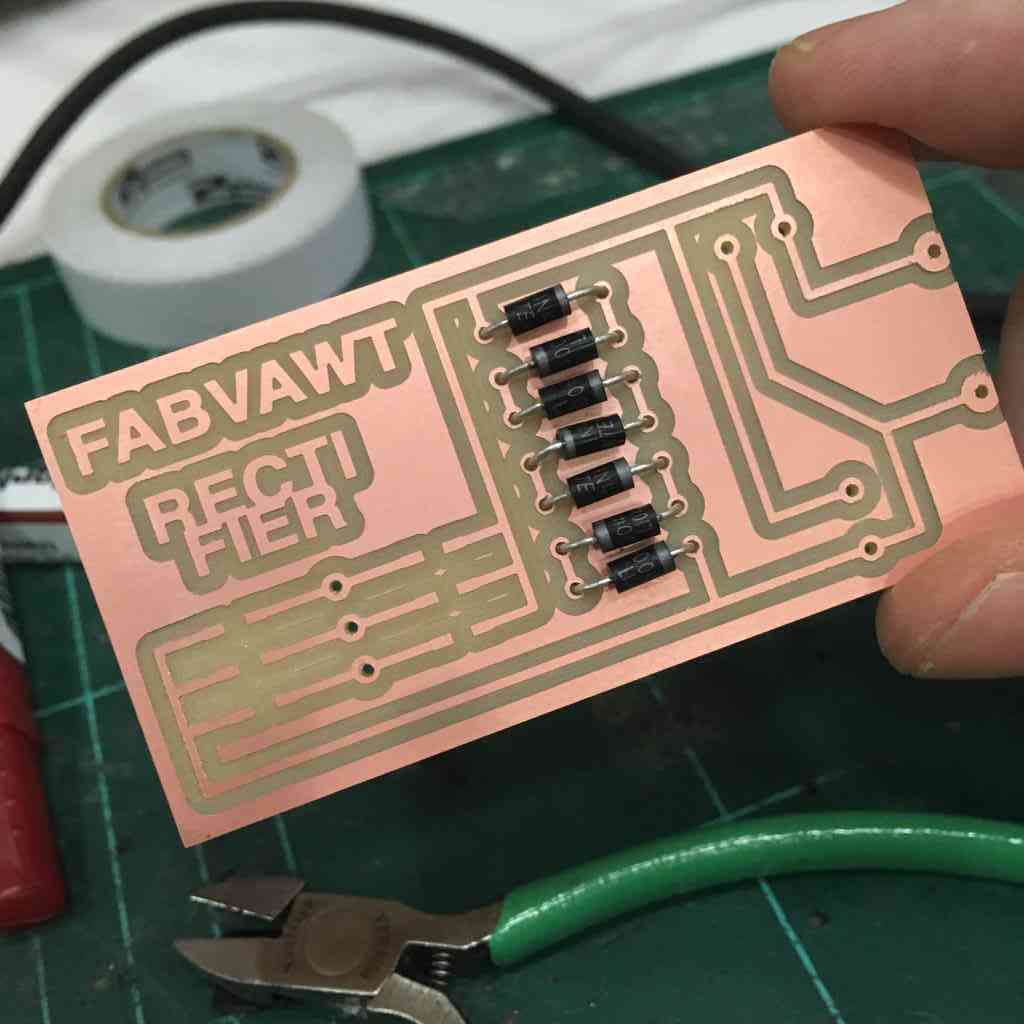
Here is my rectifier, dump load and capacitors, milled and soldered:
 |
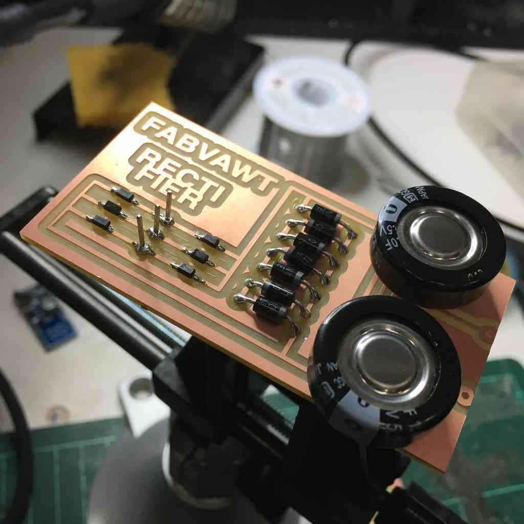 |
And here it is connected to the PFM modules. With a couple of hand spins I managed to charge the supercaps. These gave a consistent 5 volt charge for a good couple of minutes before dying down.
Designing my nikoduino
Arduino has popularised rapid prototyping electronics because it simplifies programming AVR microcontrollers via it’s integrated development environment (IDE), making complex electronics fun, easy to learn and relatively straightforward.
The Arduino hardware and software is also completely open-source and it is possible to download their schematics, modify their board designs while still leveraging the use of their IDE, extensive libraries, and wide support network. I plan to do just that.
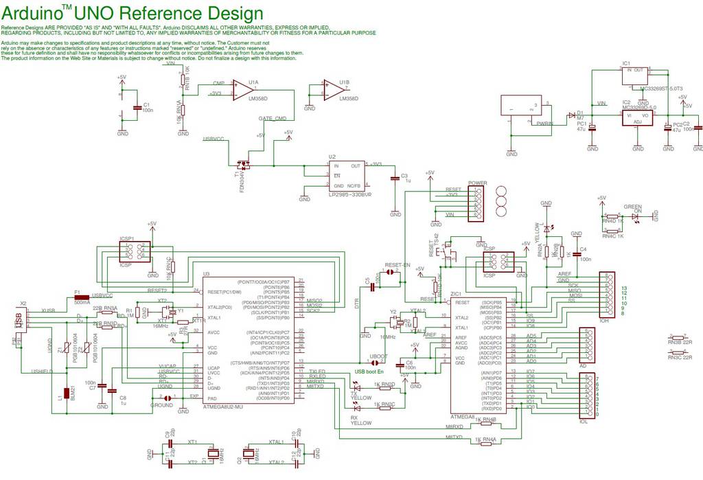
Atmega238 Schematics
The Arduino UNO uses AMTEL's ATMega328 microcontroller and it’s board layout here is the reference design. Important to notice here though, that there are two chips on the UNO board, one deals with USB to Serial communication (on the left) and the smaller one is the 28 pin ATMega328 (on the right). This is what we will be focusing on.
Satchakit
As there were quite a few uncertainties in getting started with the AtMega328P (see datasheet here) I decided to follow Daniele Ingrassia’s Satchakit which is an improvment on the earlier Fabkit mainly in that it:
- uses 16Mhz instead of 8Mhz timer
- Uses a crystal instead of resonator
- It liberates the ADC6/7 analogue pins for use
Hats off for his well documented work. If the intention of designing a board with the ATMega328 is to make the micro controller compatible with the Arduino Software (IDE) we need to burn a boot-loader with either the FabISP or another Arduino. Here below I tried both.
The whole process of loading the bootloader code and burning properly the fuses to make an ATmega microcontroller an “Arduino” is well described here.
The ATMega328P
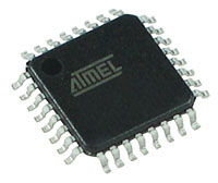
The ATmega328 or “Arduino Uno” microchip comes in various “packages” and formats that can be confusing at first. The ones we have in the lab correspond to the ATmega328/P 32-pin TQFP which looks like this and have written on it AU 1722 What does all this mean?
If you search for this component, there are many variations. Here are some clarifications:
-
The ATMega328/P is a 32KB ISP Flash memory, 8-bit microcontroller from the AVR family (same as the ATtiny’s we have been using). It has read-while-write capabilities, 1KB EEPROM, 2KB SRAM, 23 general-purpose I/O lines, 32 general-purpose working registers, serial programmable USART, and more. See Datasheet here
-
Prefers to the chips picoPower low voltage running capability, which enables the microcontroller to reduce power consumption in active and all sleep modes. -
AUmeans that it is a surface mount component, as supposed to aPUwhich is a dual in-line package (DIP or DIL) component. The latter refers to the rectangular housing with two parallel rows of pins that can be through-hole or breadboard mounted. -
1722was the year it was made, same year Dutch admiral Jacob Roggeveen lands on Easter Island and Johann Sebastian Bach composes The Well-Tempered Clavier. Or more likely a serial or manufacturing number. -
TQFPstands forThin Quad Flat Packagewhich is a surface mount integrated circuit package with thinner “gull wing” leads extending from each of the four sides to make it easy (or easier) to mill and solder. -
ATMega328 SMDis the other, surface mount version of the 328, with 2 extra analogs. This is usually the chip found on Lilypad and Nano boards and boasts two extra analogs.
For more AVR advice, I highly recommend the AVR Freaks forum. Lots of juicy tips.
Updating EAGLE libraries
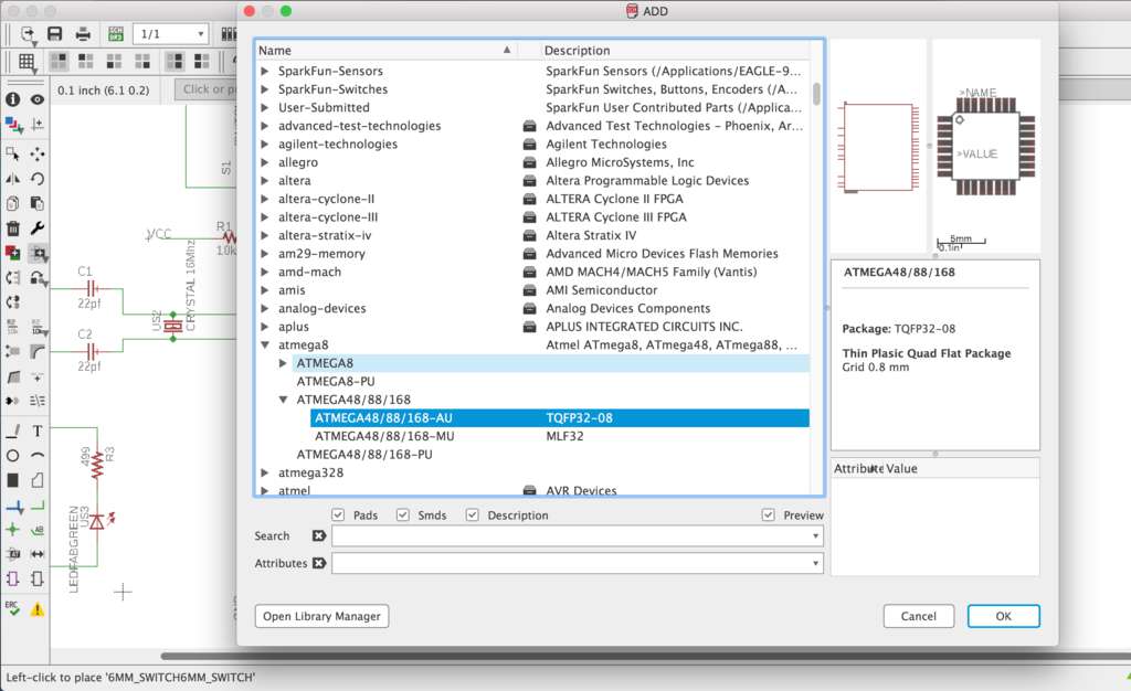
At this point I was finding the Fab library in EAGLE lacking, outdated or simply confusing with regards to the inventory we have available. I downloaded the entire Sparkfun library here to start with, as it has some other very useful components that we have in the lab. As well as this, I was desperately looking for the Atmega328P TQFP package that has a similar schematic layout as the Satchakit so that I don’t confuse too many pins as I try and figure out it’s design features. I found what I was looking for with the Atmega8 Eagle library.
-
Download or clone desired libraries from Github.
-
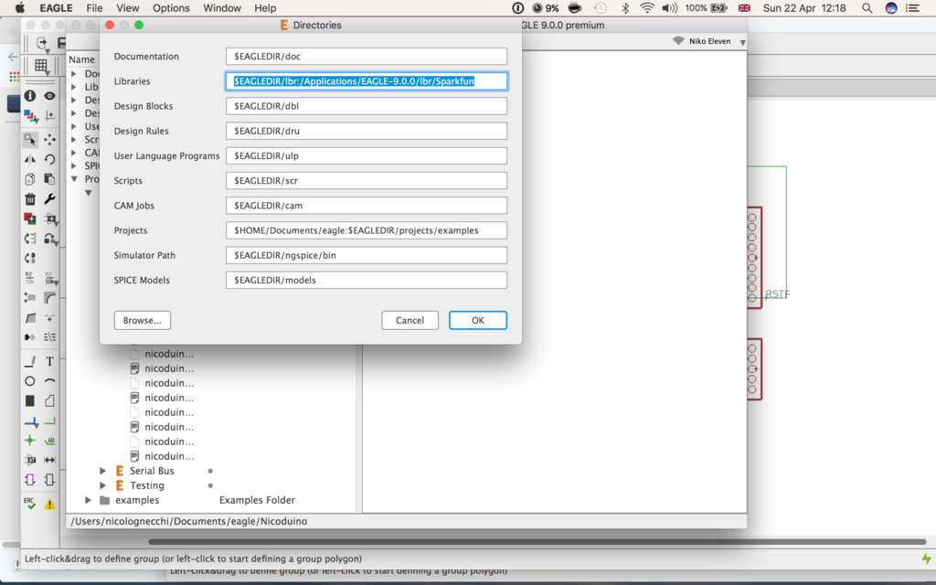
In the EAGLE Control Panel window go to
Optionsmenu and then selectDirectories. This is a list of computer directories where EAGLE looks when it populates the component libraries. -
In the
Librariesbox add a link to the directory where your new libraries are stored. If you want to keep the default EAGLE libraries and add the SparkFun library, add a colon (:) after$EAGLEDIR\lbr, and link the directory location after that, in my case I added the library it to the default app Eagle-9.0.0/lbr like so:$EAGLEDIR\lbr: Applications/Eagle-9.0.0/lbr/Sparkfun/
-
Now in the Libraries tree, you should see your new folders included. To activate them right click on the “lbr” folder, and select
Use AllorUse Noneto disactivate. -
Back in your Schematic or Board Layout view, go to menu Library and
Update All. You should now have all these new components available. For more detailed instructions this is a useful tutorial for setting up Eagle libraries.
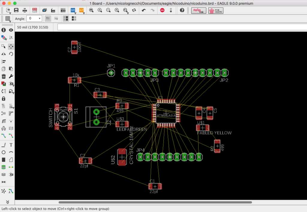
Desinging the PCB
Up to now we have been designing our boards with 16mil default traces width. This is too wide to mill with the 1/64 tool that we are using, and it is not necessary to use the super fragile 0.010 tool for this component.
I wanted to keep as many pins available for general use, so I also kept the ADC6/7 analogue pins free, and used a 16 megahertz crystal in accordance to the components we have in the lab. Make sure to check this first.
Here aligning my pins, resistors, leds, capacitors before tracing.
Modifying Eagle components
The ATmega8 library comes with a TQFP32 package, which I assumed would mean it had thinner pads. This proved incorrect.
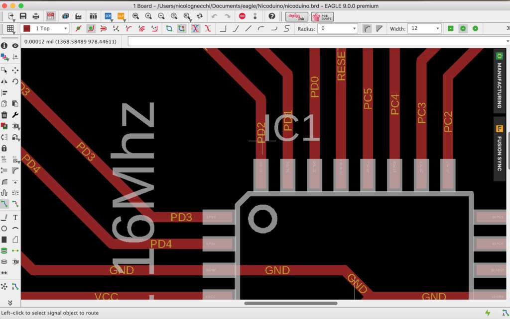
Even though I was designing with 12mil traces, as you can see here, the footprints were actually more like 16mil.
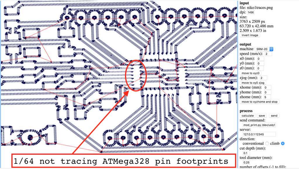
This was a problem, because once exported and uploaded to FabModules to create my milling strategy, you can see on the right that the 1/64 toolpath does not pass through the component pins.
 |
 |
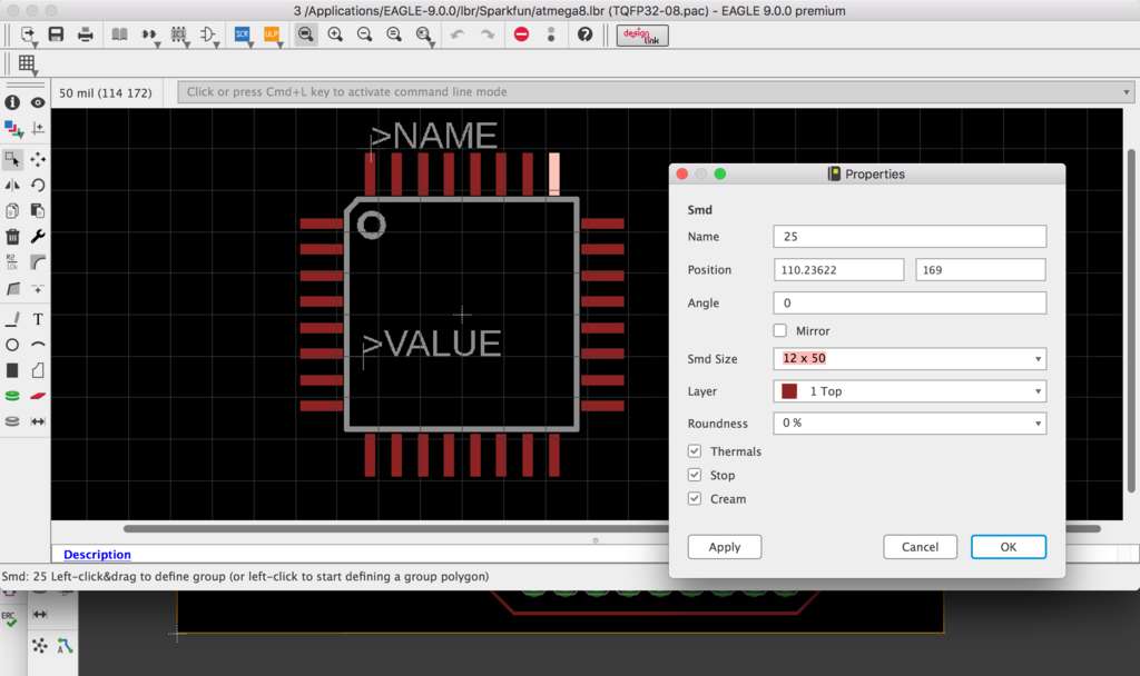
So thanks to Baptise for discovering this suuuper useful way to edit components in Eagle.
Under Library > Open Library Manager, you can edit the components which are either in your design, in use or available. Click on the component, Edit and under the Package column you click on the component (in this case the TQFP-32) and you can edit the component layers like you see below.
Here I am setting the SMD (surface mount) footprint size to 12mil (12 thousands of a inch or 0.3mm width) keeping 50mil length as default. This is the actually size of my microchip pin legs.
Make sure to Apply, it will ask you to save this as a default, and then back in board layout: Library > Update All. This should change the component SMD dimensions in the design.
After much fiddling around and trying different dimensions, this worked and I was able to mill the board using the 1/64!
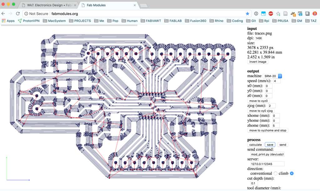
As you can see, here the is the board milled. The 12 mil traces are quite thin and on retrospect, I think it would be fine to design the “tentacles” of the SMD mount in 12 mil and doing the rest in 16 mil, if conserving board space is not an issue.
Sweep soldering
When microcontroller pins are too small to solder individually, the way to do it is using “pin sweep” method of soldering. This goes like so:
-
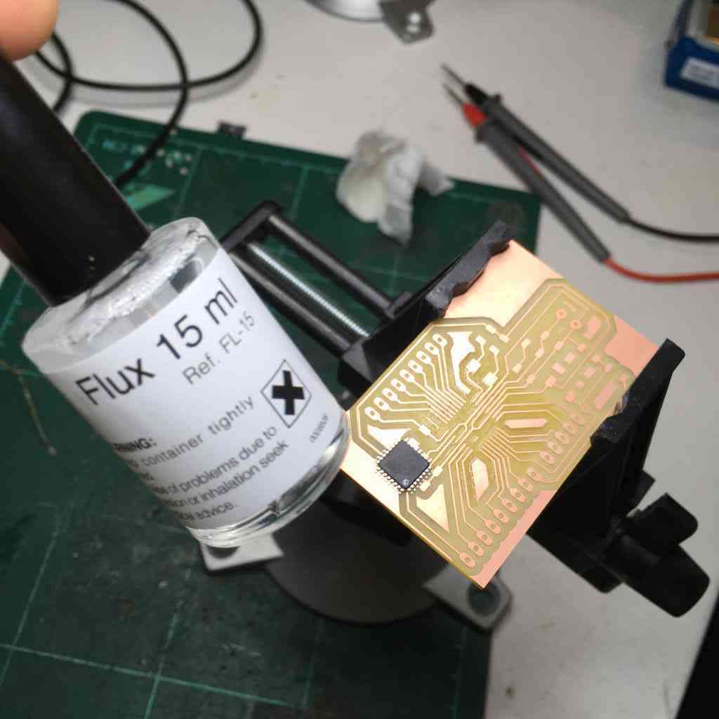
Apply a Flux to the pin traces. Fluxes facilitate soldering (also brazing and welding) by removing oxidation from the metals to be joined.
-
Make sure you correctly align the chip (look at the schematic!!) and using tweezers and magnifying glass if possible, carefully place the component so it sits flush on the traces.
-
Wet the soldering iron, and carefully solder two opposite corner pins of the micrcontroller to “pin down” the chip. Don’t worry about the solder spreading, keeping the component aligned with the traces is more important.
-
With the chip pinned down, wet the iron again and liberally “sweep” all the remaining pins making sure that they are heated long enough to suck up the solder.
-
Place a wick (a weave of copper wire) on your soldered pins and iron above to wick away the excess solder. This should leave clean and shiny soldenred pins.
Here is a good tutorial for this method.
 |
 |
Also as you can see I did not mill my through holes, with my outline. This would have required an extra milling strategy, and instead I did these manually using the dremel tool we have in the lab. This gives one the sadistic sense of power dentists must feel when doing a root canal.
 |
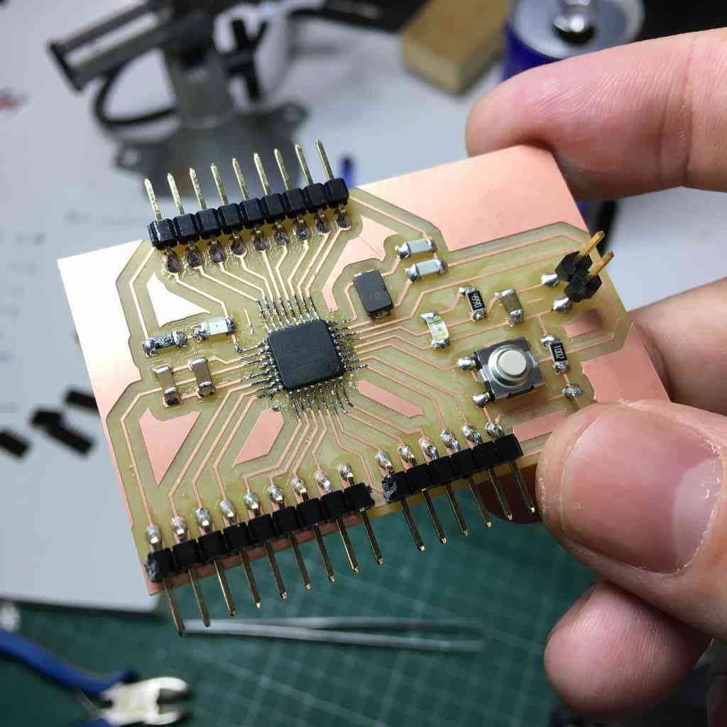 |
After checking all my connections (make sure to do this carefully with every pin) I was ready to program.
Programming
First things first, make a good diagram labelling your every pin and port. See below with corresponding Arduino (unofficial) pinout diagram.
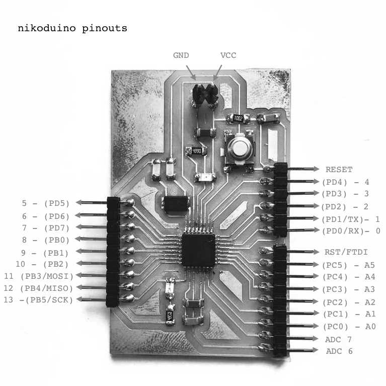

The pins on this PCB were kept exactly like the Arduino UNO board so that I can use the IDE without any trouble to rapid prototype. To upload sketches to the ATMega328 via the serial port (like you do using the USB with a standard Arduino) it first needs a bootloader.
In electronics production week we learnt that a bootloader is basically a program that loads an operating system when a computer is turned on. For Arduino, the bootloader supports re-programming the program memory (or Flash memory) over the serial ports (rx and tx) without needing a dedicated programmer like our FabISP all the time.
Bootloader tradeoffs
There are a few reasons that Neil keeps repeating why he programs his AVR’s in C-code directly. Since the Arduino bootloader runs before your code, this delays executing the “real” program C code. The Arduino Uno Bootloader also takes up 508 bytes of memory which if might be an issue if you have a big program.
The bald engineer describes this well. Also good reading material is:
E Fuses?
At first I followed Satcha’s example by burning the Arduino bootloader using my FabISP programmer like so:
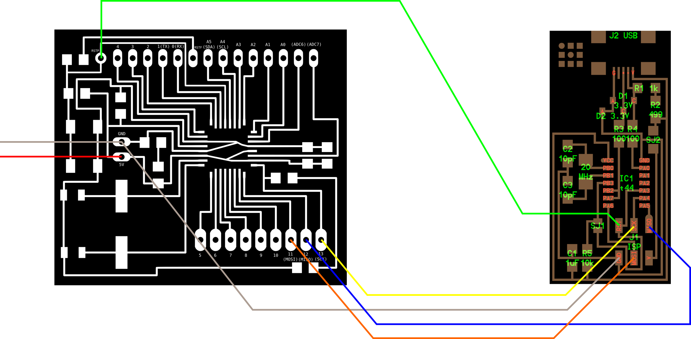
As you can see, we are simply connecting the MOSI, MISO, SCK (CLOCK) and RESET pins with jumper wires.
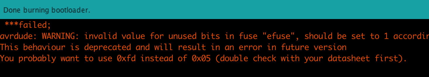
Then in the Arduino IDE, I selected the USBtinyISP as programmer, ArduinoUNO as board, and under Tools > Burn Bootloader
The Led’s flickered, the universe expanded, and after a second or two I got this contradictory success message with a big fat warning caveat:
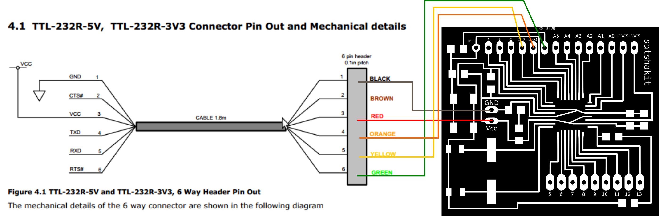
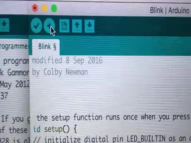
I tried uploading the basic blink sketch. So I was able to upload the sketch using the FabISP, but this defeated the purpose of having a bootloader. So I burnt the bootloader again, this time using another Arduino board as an ISP and then connected the FTDI (USB to Serial port connector) as how Satcha illustrates:
Now attempting to upload my blink sketch I wasn’t getting any luck, all I was getting in the IDE was:
avrdude: stk500_getsync(): not in sync: resp=0x00
avrdude: stk500_disable(): protocol error, expect=0x14, resp=0x51
This seemed to suggest there was no communication with the board whatsoever. I tried changing to see if designating the board as an “Arduino mini” or “pro” would work but no luck there either.
Changing Bootloaders
After a fair bit of head scratching I stumbled upon Nick Gammon’s amazing site where he has customised his own Arduino bootloader which specifically sets the EFuse = 0xFD. I decided to give this a go, downloaded his bootloader sketch from Github.
- Make sure your board is wired to the Arduino ISP as above
- Upload the Gammon’s ATMega_Board_Programmer sketch
- Open the serial monitor and follow the prompts
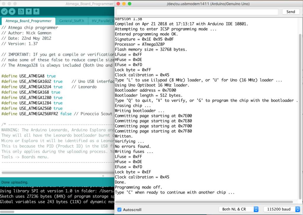
Nota Bene: NL & CR are selected and 115200 Baud Rate for serial comms. Otherwise you see gibberish.
Serial Programming
Now connecting the FTDI again as above, BOOOM!
Lessons learnt
There is a lot to be learnt about how the Arduino bootloaders work in general. After reading through the ATMega328P datasheet (page 277), and looking over Mr. Gammon’s bootloader code, this seems to be about how the Flash memory is organised between it’s bootloading section and application section.
-
The size of the different sections is configured by the BOOTSZ Fuses as shown in Table 24-7 on page 289 and Figure 24-2.
-
These two sections can have different level of protection since they have different sets of Lock bits.
My laymans understanding up until now is that this is how you configure the Read-While-Write Self-Programming mechanism for downloading and uploading program code by the MCU itself.
I need to investigate this further. For now, let’s plug and play.