Wk7. Electronics Design
-
Individual assignment: redraw the echo hello-world board, add (at least) a button and LED (with current-limiting resistor) check the design rules, make it, and test it. For extra credit measure its operation and simulate its operation.
-
Group project: use the test equipment in your lab to observe the operation of a microcontroller circuit board
What’s in electronic design?
Electronic design workflow generally involves:
-
Designing a Printed Circuit Board (PCB) circuit using an Electronic Design Automation (EDA) software. In this case the two options I decided to try are Eagle and Kikad.
-
Placing the components in a schematic and connecting them to each other, as well as a power and ground source.
-
Routing the traces between the components and laying out the board. Exporting a PNG file of the traces that can then be converted into machine code to mill the PCB.
-
Stuffing and soldering the PCB, check the connections using an multimeter, and proceed to program. What’s in Neil’s board?
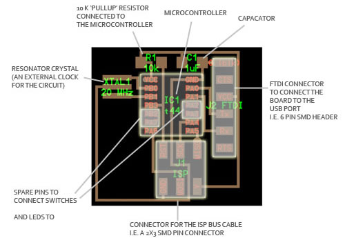
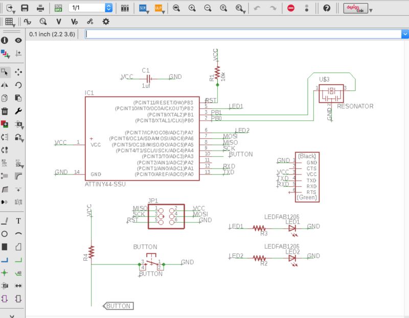
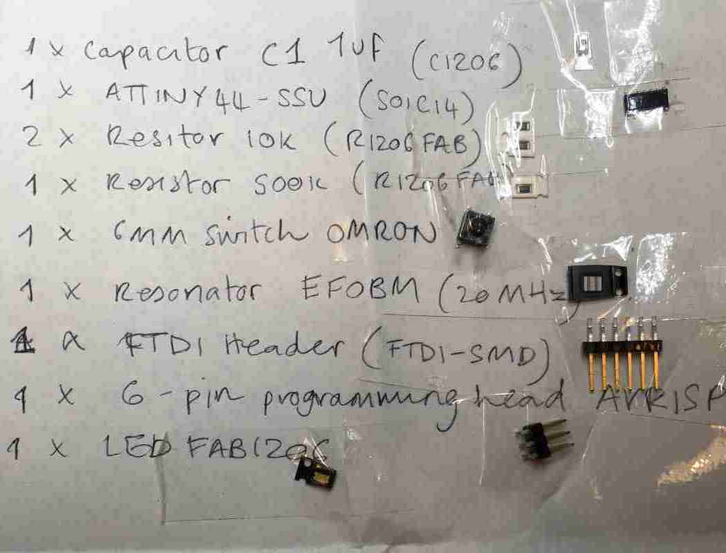
I think it is good to first have a look a Neil’s board, and get an understanding of what components are in it, why and what they do. I found great documentation and help from Pip, a past fabstudent from whom I sourced this image. Thanks Pip! Going clockwise up from the ATTiny44, this is what we have:
-
Microcontroller: this is an ATtiny44 programable chip that controls all the parts on the board and is programmed from the computer.
-
Pull-up resistor: this 10K resistor keeps the power flowing into the microcontroller steady near VCC or zero and needs to be connected to the VCC pin on the ATtiny.
-
Capacitor: this is a device used to store electric charge, consisting of one or more pairs of conductors separated by an insulator. This will help filter devices to remove voltage or signal spikes in our circuit.
-
FTDI Connector: This will connect the circuit to the computer to both program and power the board. It’s VCC and GND pins need to be connected to the respective VCC and GND circuits on the board, and it’s Tx and Rx pins connect to the two free pins on the microcontroller.
-
SMD Bus Connector: Takes in information from the FabISP and connects it to certain pins on the Microcontroller to program the board. This also needs to be connected to VCC and GND on the respective pins on the Microcontroller, and the other pins need to be connected to free input and output pins.
-
Resonance crystal: This is an external clock for the circuit. It needs the input traces to be connected to two pins on the board and the ground trace to the GND circuit.
-
Spare pins: these are the free pins on the chip to which we must connect our button/switch and LEDs.
Getting Started with Eagle
For convenience sake, and because most of our instructors are familiar it, I choose to do this assignment in Eagle. EAGLE is owned by AutoDesk and stands for Easily Applicable Graphical Layout Editor and is free on a limited licence, but this is enough for what I need to do. With more time, I would like to explore KiCad as it is free and open source.
To get myself started, I followed the Fab tutorial here. Eagle can also seem clunky and annoying at first, so I recommend Jeremy Blum’s tutorials to get the hang of the tool. Also essential reading are the Sparkfun Eagle tutorials, how to read a schematic and integrated circuits.
After downloading and installing Eagle, I downloaded the fab library (fab.lbr) file and drop it into the libraries folder in Mac OS under, Applications/Eagle/lbr. To activate the library launch Eagle and go to libraries/use.
Schematics
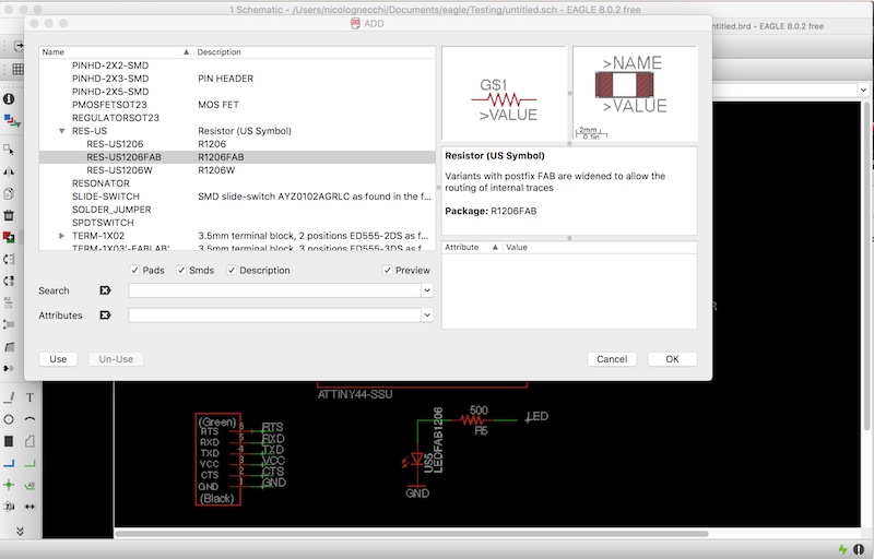
Once inside Eagle, I created a new project, and new schematic. This layout allows me to start adding in my components. To do this I used the add button on the left toolbar, which pops up the library window with millions of components. They are listed alphabetically, so under the fab library I was able to locate and choose all the components for my board. See below:
- 1 x 6MM_SWITCH OMRON SWITCH
- 2 x RES-US1206FAB
- 1 x 500k RES-US1206FAB
- 1 x ATTINY44-SSU
- 1 x 6 pin header AVRISPSMD
- 1 x 1 uF CAP-US1206FAB
- 1 x LED 1206
- 1 x 6 pin header FTDI-SMD-HEADER
- 1 x 20 MHz RESONATOR
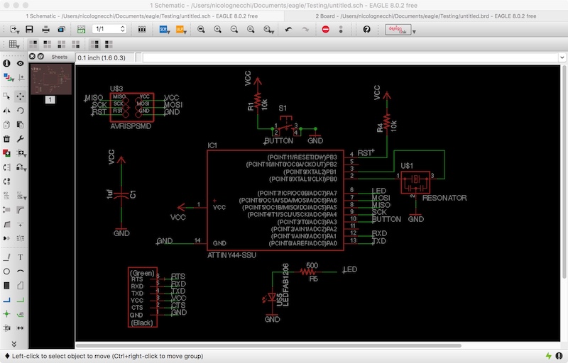
Connecting the components on the schematic is not so intuitive, but once you get the hang of it, it’s pretty straight forward. To do this we use the NET tool.
You don’t need to draw direct lines to each pin or connection as this will inevitably lead to cross-overs and spaghetti junctions. Creating a path with the NET from a component, and naming it will suffice. Do this by right clicking the path and selecting NAME. Remember to LABEL the path the same way.
NET -- NAME -- LABEL
Some components will need connect to both ground GND and power VCC so it is normal to have more than one connections to both VCC and GND.
It is also good practice to put values on our resistors and capacitors, as in this exercise we will be using different size resistors with the LEDS and they are easily confused.
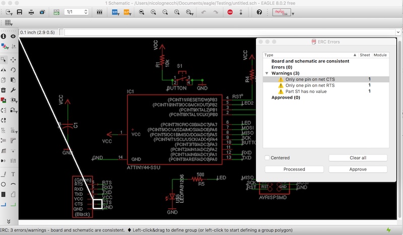
Finally, in TOOLS: ERC (electronic rules check) I made sure my board will actually work. When I first did this it presented a few problems that I had to remedy. See here:
Laying out the circuit
When you open up the board layout, Eagle should have linked it to the schematic. If you by mistake opened a board before the schematic it may not recognise it. The connection points should show up as red rectangles in the board window and the connections between components should appear as yellow lines.
I now re-arranged the components on the board using the select and the move tool. Once selected, right clicking will rotate the selected component. Bring the components as close as possible to their connecting parts. By using the move tool and you can also move components in groups.
Once components are more or less aligned and as close to their corresponding connections, draw the traces using the traces tool. Click in the centre of a component to start a trace, then right-click to change angles.
The traces will snap according to a preset grid, which is annoying when trying to route through narrow spaces like under the ATtiny. Type the command: GRID FINEST to bring allow for more tolerance and then rest it with GRID LAST.
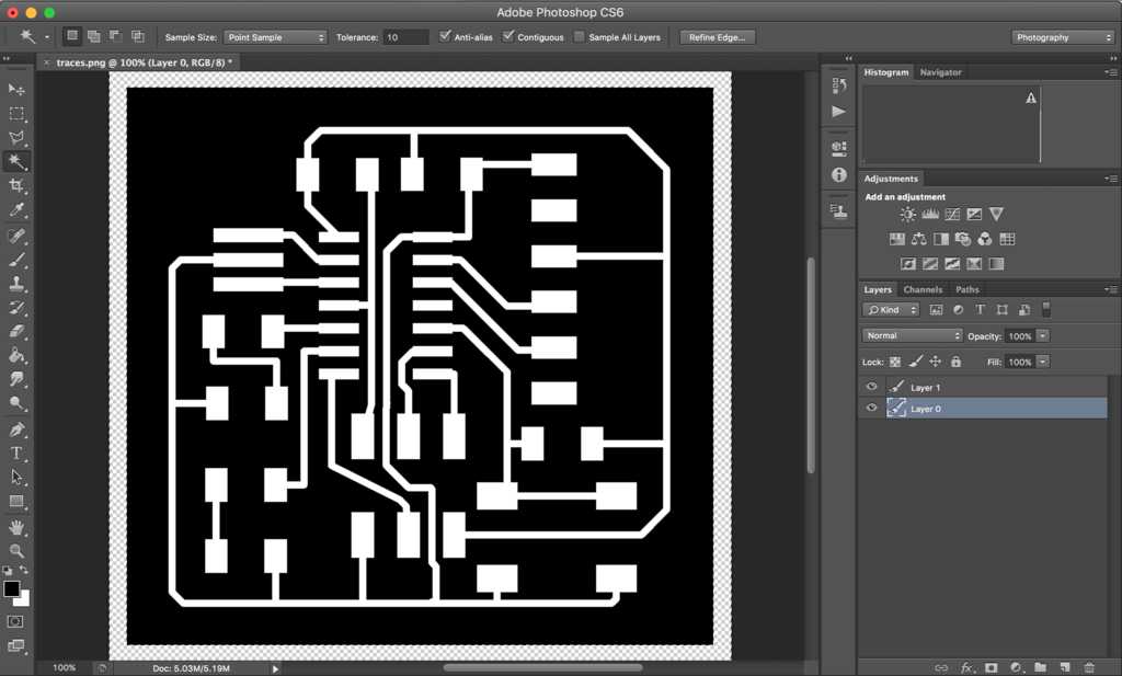
This part took some patience. Below you can see how I redesigned the board added two LEDs and corresponding resistors.
 |
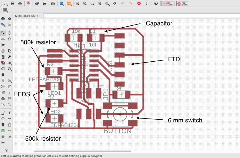 |
NOTE: It is good to turn the various layers on and off using the layers tool, at the top left of the toolbar. This allows you to see which component is which, or can turn off labels to help you concentrate with those traces.
Fails, errors, lessons:
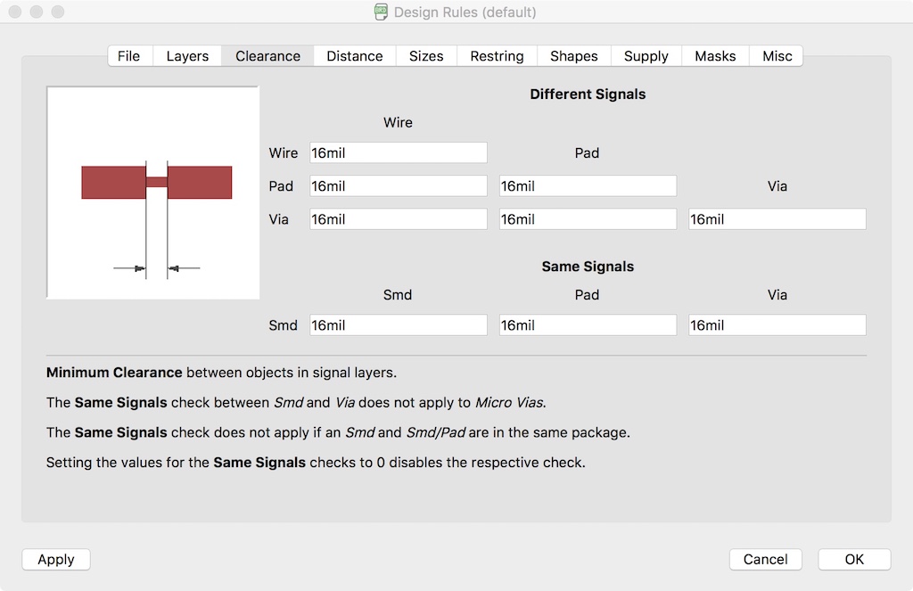
Using the DRC or design rules check (back in board view) I made sure all the default settings were in 16 mil. This showed me multiple errors where the traces were too close together, and where I did not have them properly connected. I also realised that I hadn’t been using the fab resistors which are of a different pad size, so I had to go back and replace those.
At first I also had mis-connected the RXD and the TXD between pin 12 and 13 on the Micro controller and FTDI connector as these all look the same, and my dyslexia doesn’t help. MOSI and MISO are also easily confounded. I recommend doing a thorough pin to pin check through the circuit once you are done tracing.
Export, Import
A number of our class MACOS users had trouble getting a good enough resolution PNG when exporting an image directly from EAGLE. I tired using the CAM PROCESSOR file: Cam Processor to create an EPS file. To do this make sure in Eagle board view I only had top, pads and vias selected. Then when setting the file location to save, make sure to write the extension .eps before clicking PROCESS JOB.
This however, failed to work so I ended up exporting from Eagle as a PNG as usual, recording the file dimensions and resizing the image (not the canvass) in Photoshop.
The process is as follows:
- In Eagle (Board Layout) File > Export Image:
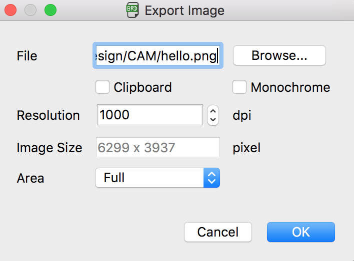
- Select where you want to save the image, add a resolution greater than 500dpi (on the safe side I go for 3000) and make sure you have Area > Full. Also select Monochrome as this will export the image in black and white.
- RECORD the image size in a screen shot like above.
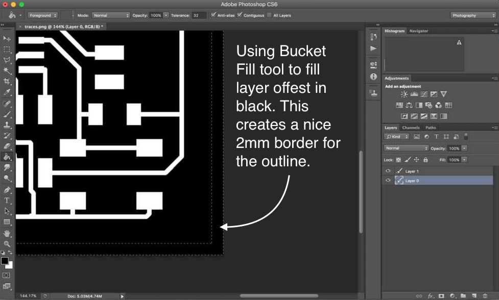
Making an outline in Photoshop
- Open the .png in Photoshop and go to Image > Mode and make sure the image is set to RGB Color.
- Select the image and copy background to layer.
- Go to Image > Size and reset the pixel dimensions to the ones you recorded. Width and height should be interlinked so by changing one you should get the other.
- Create new layer
- Got to Image > Canvas Size and putting the units in millimetres I expand the canvas by 2mm in each direction.
- Return to original Layer, using the Magic Wand tool I selected the offset gap left between the two canvasses. Returning to Layer 2 used the Bucket Fill tool to fill this area in black. This creates a nice 2mm border for the outline.
- Then, still in Layer 2, deselect (CMD-D) and change the Fill Bucket color to white and fill the inside of the Layer 2 black border in white.
- Make sure the original layer sits above the Layer 2 and turning on and off the eye view button, save each layer as individual .png
 |
 |
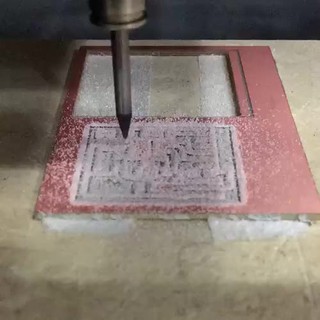
Milling on the Roland Modela
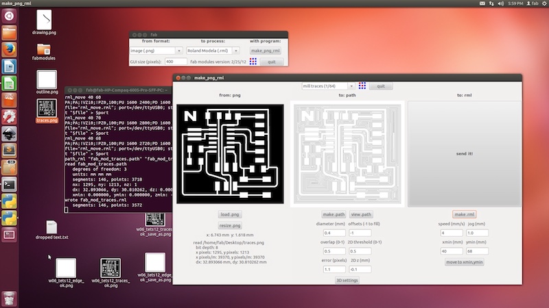
Milling on the Roland Modela a little more tricky than the Roland SRM-20 I used in Week4. It runs on our Linux Ubuntu desktop which means you have to run FabModules from the Terminal which takes getting used to.
 |
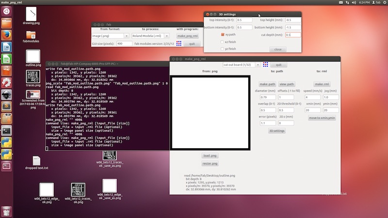 |
Once launched, the Python program of Fabmodules works much the same as the online one. Select the .png image in the format and then in process select our friend Roland Modula. Then click: make.png_rml. The PNG (let’s start with our traces using the 1/64 bit) should appear on the left. When you click MAKE:PATH the milling outline will appear. As with the Roland Mill, you can define the offests, or have none by sticking to -1.
Modula is not as friendly setting the X/Y as the fancier Roland. Basically, you have to add values in the Xmin and Ymin boxes, under the to:rml panel. Depending on where you stuck your PCB on the mill floor this will vary. The Z axis can only by found using the arrow keys on the machine. Once you have the X/Y more or less, bring down the Z (with the right size bit added a-priori) then as with the Roland, un tighten and gently bring the bit down to board.
With all three axes defined, only then select: MAKE RML. This will set the 0 axis. When you are ready, hit SEND IT in the right panel and the machine will start.
Milling and Stuffing
First, make an “organised” list of all your components. Name them and MAKE SURE YOU CHECK YOUR RESISTOR VALUES.
Now I really recommend to put on some concentrating beats and get soldering!
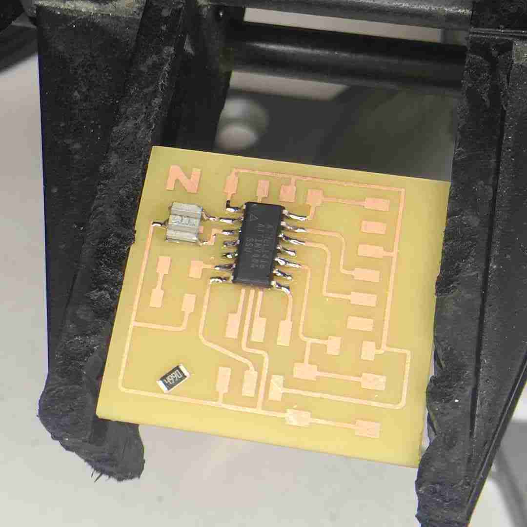 |
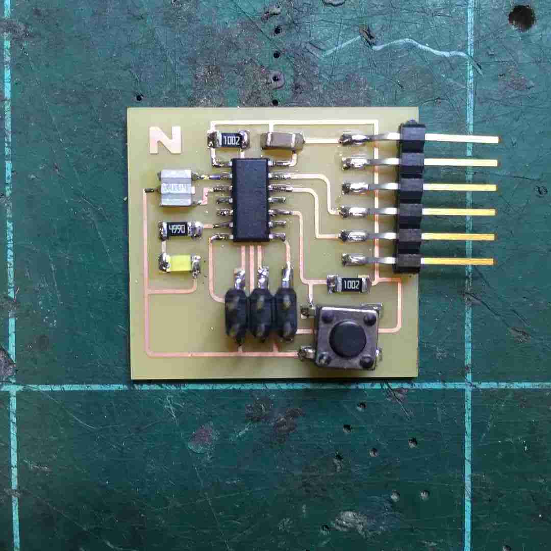 |
Dry testing on the digital multimeter (DMM)
First step before programming, we must use the digital multimeter to check that all our connections are working. The multi-meter is your best friend because it will save you going crazy debugging if you know that your circuit is not working as it is supposed to.
Checking for continuity
- Turn the dial to Continuity Test mode ( continuity ). It will likely share a spot on the dial with one or more functions, usually resistance (Ω). With the test probes separated, the multimeter’s display may show OL and Ω.
- First insert the black test lead into the COM jack.
- Then insert the red lead into the V Ω jack. When finished, remove the leads in reverse order: red first, then black.
- With the circuit de-energized, connect the test leads across the component being tested. Usually it is good to check your VCC connections and your ground connections going, and then the connections to each pin on the micro-controller.
- The digital multimeter (DMM) beeps if a complete path (continuity) is detected. If the circuit is open (the switch is in the OFF position), the DMM will not beep.
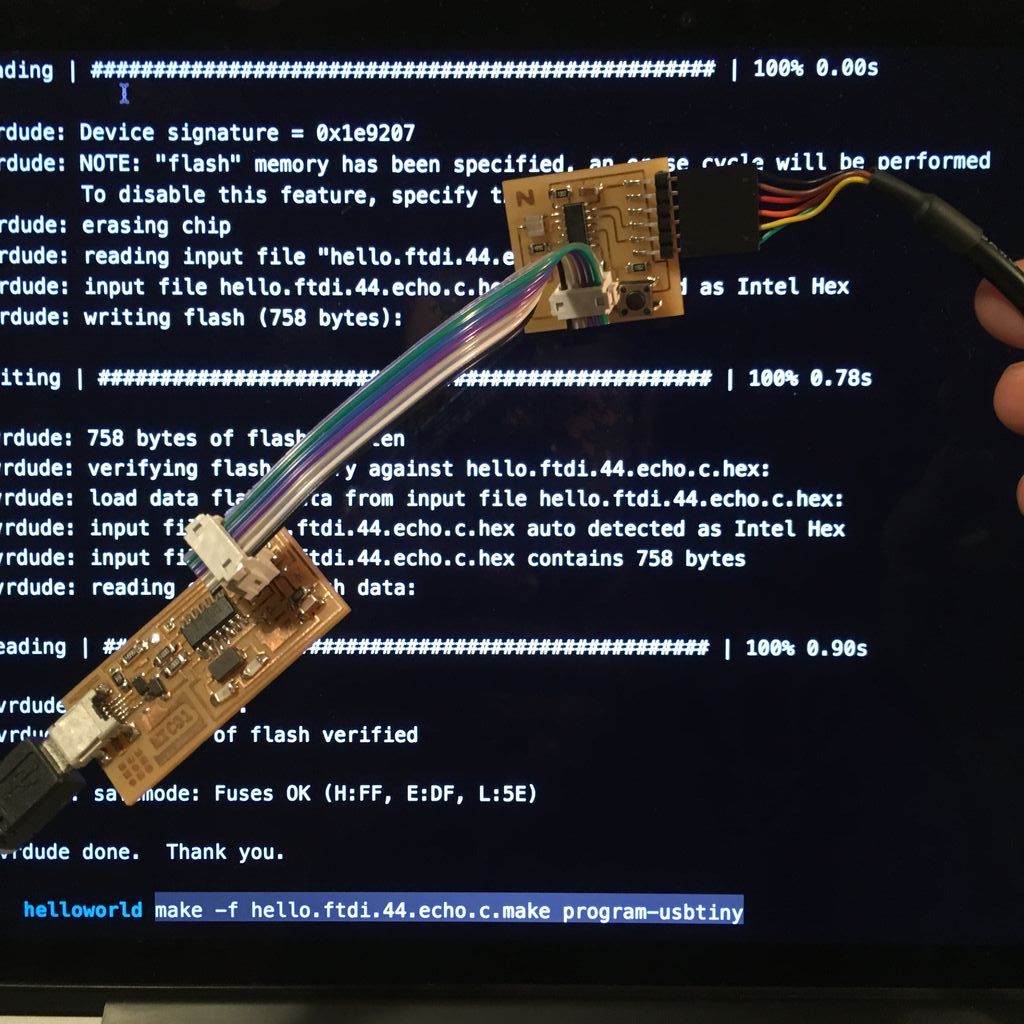
Programming Hello World
The first step is to connect the newly created Hello Board to the computer using an FTDI ←→ USB cable. The FTDI head looks like this:

TO check which usb port our hello board is connected in MacOs go to terminal and run:
$ ls -l /dev/cu*
This gives me:
/dev/cu.Bluetooth-Incoming-Port
/dev/cu.usbserial-A505DVC9
This is my computer telling me what peripherals I have connected. I am looking for /dev/cu.usbserial-A505DVC9.
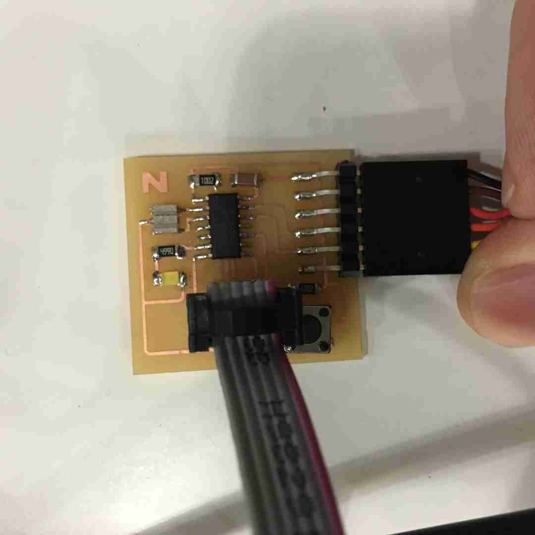
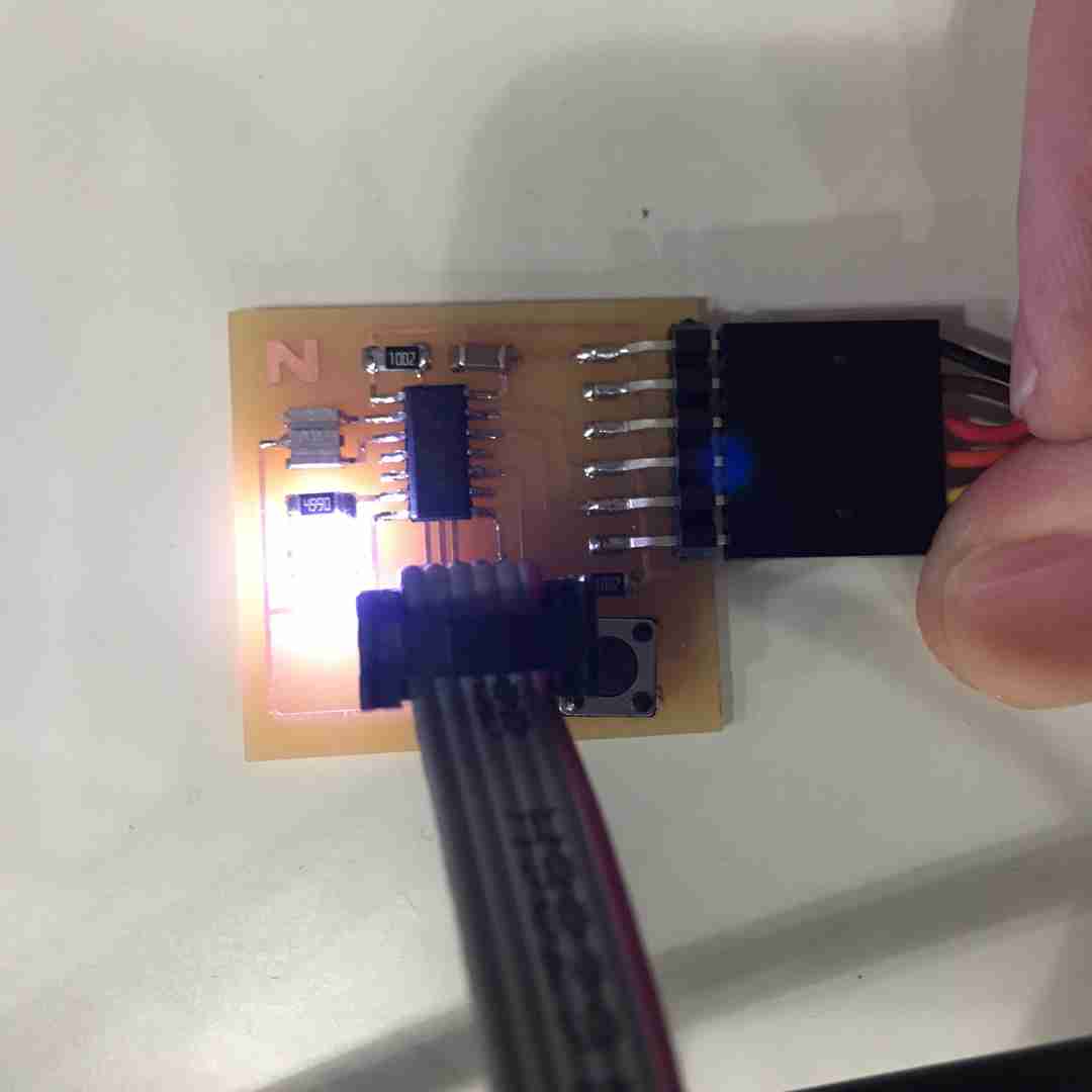
Connecting the ISP programmer
Now connect the ISP programmer (we made in week 5) to the other USB port. Use the ribbon cable to connect the FabISP and the Hello World board using the two six-pin headers soldered on each. Usually there is a twist in the cable because GND and VCC need to be aligned. Check the board layout from Eagle to make sure. It looks something like this:
Notice the black of the ribbon cable is connecting to the same side of the six pin header of both ISP and Hello boards.
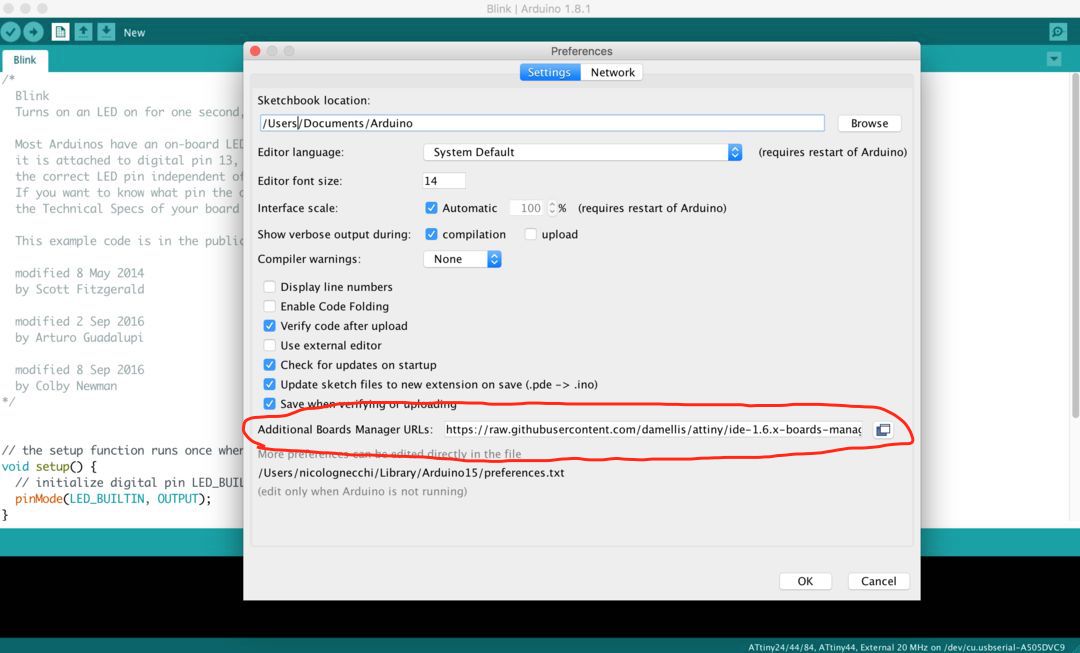
Blink Test on Arduino
For a very first blink test I will use Arduino Integrated Development Environment. If you have not downloaded Arduino IDE do so NOW. This has a number of prebuilt sketches for us to use. However, first we need to enable Arduino Boards Manager to find the ATtiny board we are using.
- Arduino → Preferences and look for the Additional Boards Manager URL’s. This is going to enable Arduino Boards Manager to be able to find the ATtiny boards package.
-
Here under
Additional Board Manager URLsadd this url:https://raw.githubusercontent.com/damellis/attiny/ide-1.6.x-boards-manager/package_damellis_attiny_index.json -
Go to Tools → Board → Boards Manager… And select the Attiny package. At the time of writing this the version was 1.0.2.
-
Now you should be able to see the ATtiny24/44/64 entry under Tools → Boards. This allows Arduino to speak to the ATtiny44 microcontroller on our our Hello Board.
-
Select the processor by going to Tools → Processor and selecting ATtiny44.
-
Select the clock by going to Tools → Clock and selecting External 20 MHz.
-
Next we have to burn the bootloader baby. Select the ISP programmer from Tools → Programmer. Here under Processor you should see Attiny44.
Now I am ready to program my board.
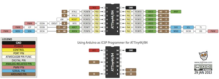
This diagram is SUUUPER helpful to figure out which pin to define within the Arduino sketch.
Here is my Arduino blink sketch:
#define LED 7
#define BUTTON 2

void setup() {
  pinMode(LED, OUTPUT);
  pinMode(BUTTON, INPUT);
}

void loop() {
  if (digitalRead(BUTTON) == LOW) { // IF the button is NOT pressed
      digitalWrite(LED, HIGH);   // turn the LED on
  } else {
      digitalWrite(LED, LOW);   // turn the LED off
  }
}
Whoop Whoop! Is it on? Is it working?
 |
 |