Week 6: Electronics Design
For this week's assignment, we will explore the world of PCB design using KiCad software.
Group Assignment
For this week's group work, we will test multiple types of electrical signals, including:
- Digital Signal
- Analog Signal
- PWM (Pulse Width Modulation) Signal
Here is the full group assignment documentation:link

Individual Assignment
For this week's assignment, I tried multiple circuits, including a sample PCB for my final project.
0. What Is a PCB?
A printed circuit board (PCB) is a flat board made of insulating material, such as fiberglass or plastic, with conductive pathways etched or printed onto its surface. These pathways, often made of copper, allow electrical components to be connected and communicate with each other. PCBs are used in almost all electronic devices, from simple gadgets to complex systems, providing a compact and organized way to connect components and ensure reliable electrical connections. They can have multiple layers to accommodate more complex circuits and are essential for the functionality of modern electronics.

The PCB design process typically involves several steps, including schematic capture (creating a diagram of the circuit), layout design (arranging components and routing connections), and manufacturing (producing the physical board). PCB designers use specialized software, such as KiCad, to create and optimize their designs before sending them for fabrication.
Here is a good reference for learning more about PCBs: link.
1. Download KiCad
KiCad is free and open-source software used for designing electronic circuits and printed circuit boards (PCBs). It allows users to create schematics, place components, route electrical connections, and visualize the final board in 3D before manufacturing. KiCad is widely used by students, makers, and professional engineers because it provides powerful PCB design tools without licensing costs.
You can download KiCad software from its official site.
2. What I Designed
I designed three PCB circuits: a simple three-blinking-LED circuit, a DHT11 circuit, and a sample PCB from my final project.
- Blinking LEDs circuit
- DHT11 PCB circuit
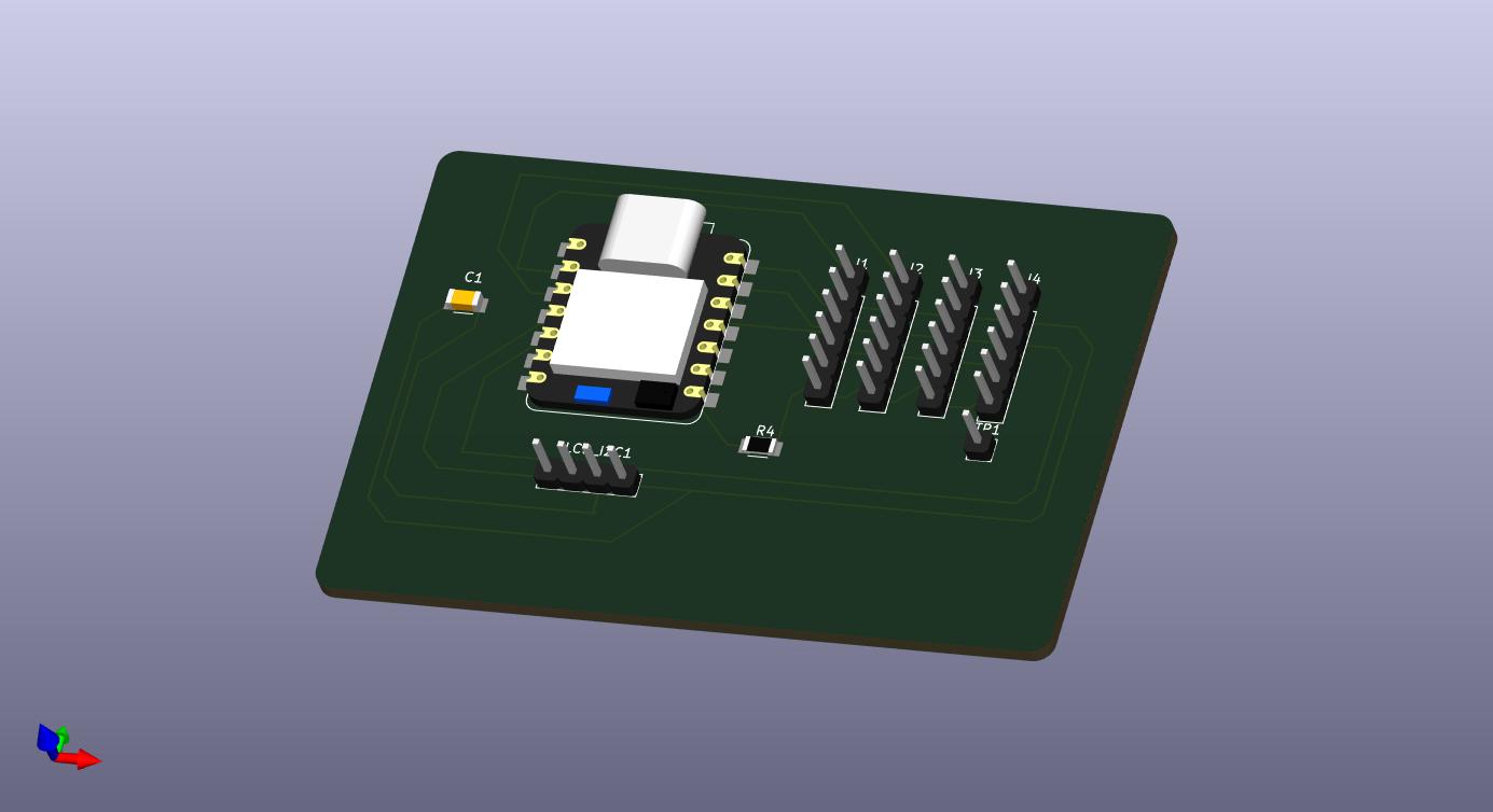
- Final project sample PCB circuit
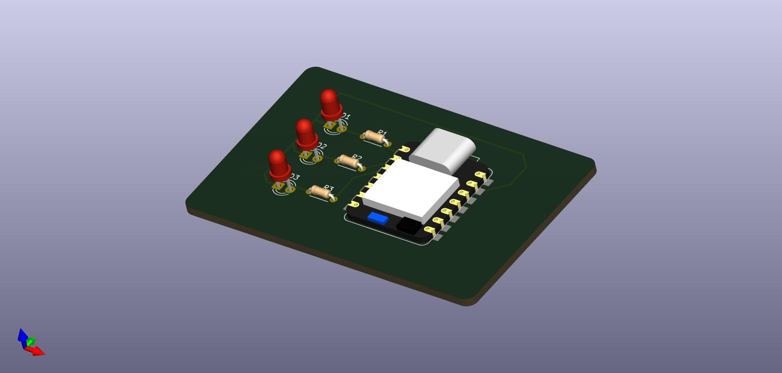
Here is the KiCad project file for the blinking LEDs circuit: Download
Here is the KiCad project file for the DHT11 circuit: Download
You can see my conversation with Gemini, which helped me understand how to build a PCB for my final project: link
Here is the KiCad project file for the final project sample PCB circuit: Download
3. Process
- First, I chose what I wanted to design and decided which components I would use.
- Then, I chose which software to use for the design.
- Now I will create the schematic design.
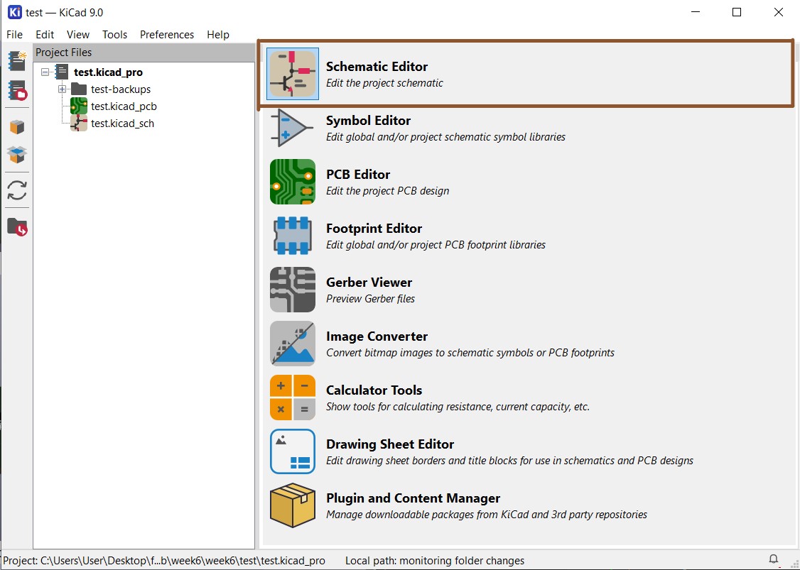
- First, I selected Schematic Editor to start the schematic design.
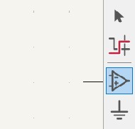
- Then, I started adding components by clicking the Place Symbol button and selecting the parts I needed from the library.
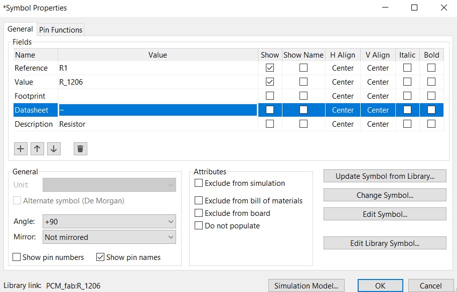
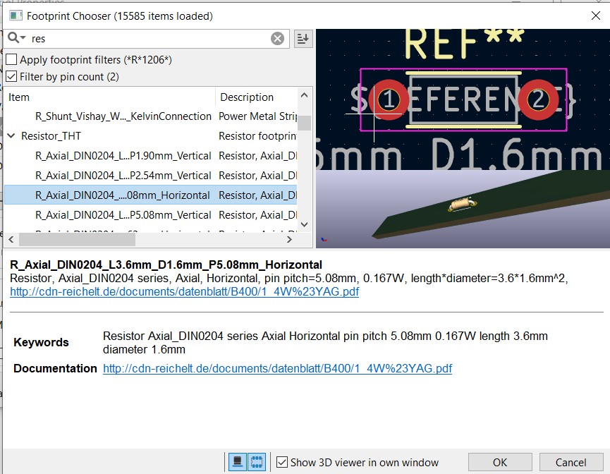
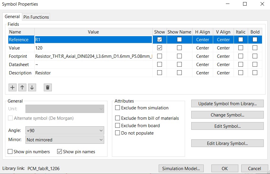
- After adding the components, I verified their values and footprints by double-clicking each component and checking its specifications.
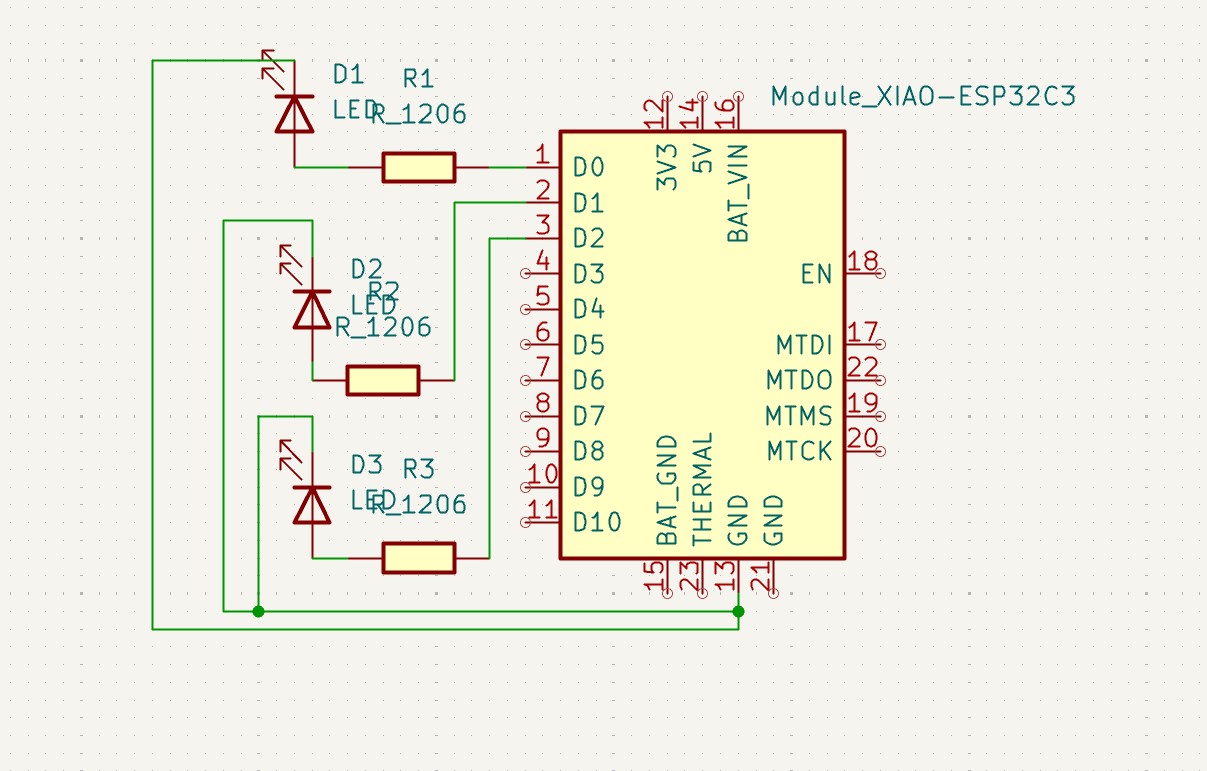
- After adding all required components, I connected them using the Place Wire tool.
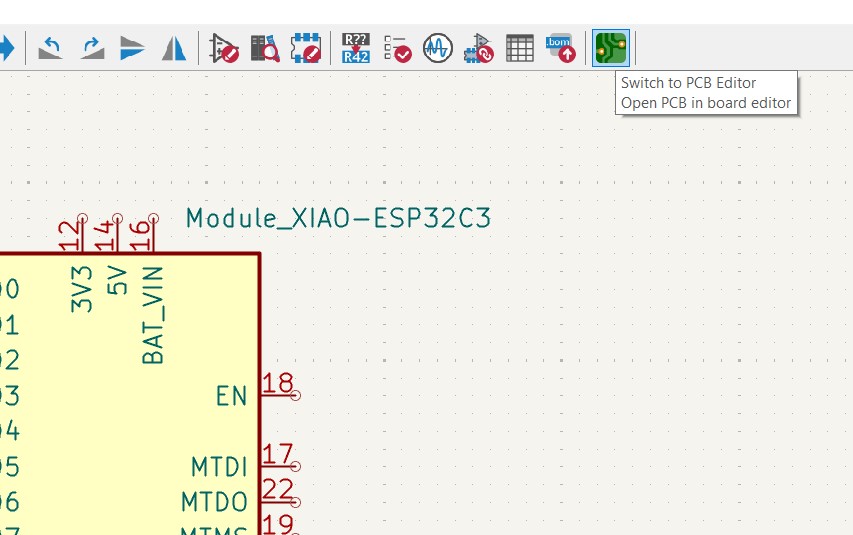
- After finishing the schematic design, I moved to PCB design.
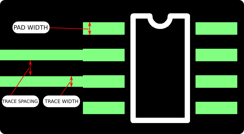
- First, I set the PCB design rules in Board Setup.
- Minimum PCB clearance (trace spacing in the image) is the smallest spacing between conductive elements (traces, pads) to prevent arcing and shorts. It is typically 4–5 mils, depending on the tool diameter used by the fabrication machine.
- Minimum trace width is the narrowest copper path allowed for current capacity and manufacturing constraints, often 3–4 mils.
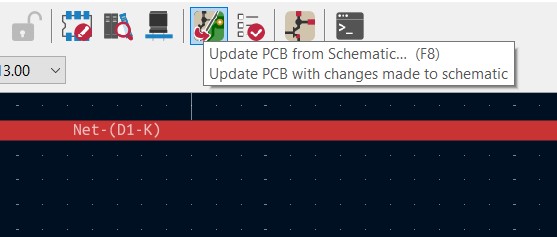
- Then, I updated the PCB based on the schematic by clicking Update PCB from Schematic.
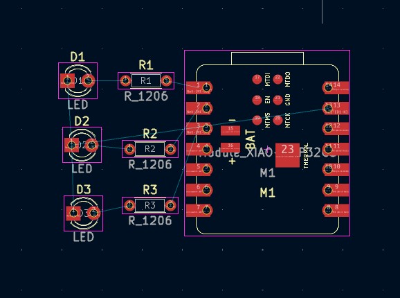
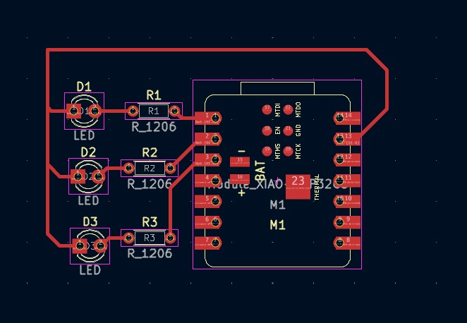
- The PCB was updated from the schematic, but it was not arranged properly, so I arranged the components.
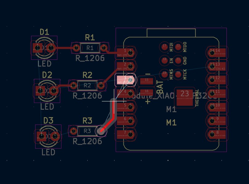
- After arranging the components, I routed the connections using the Route Tracks tool.
- After routing, I checked for errors using the Design Rules Check tool.
- Here is the final PCB design for the blinking LEDs circuit.
I created a new project and gave it a name to start the design process.
This step involves creating a diagram of the circuit using the selected components and setting specifications such as values and footprints.
You can enable the 3D view to check component footprints and confirm they are correct.
I made sure to set everything correctly for each component.
In this step, I arranged the components on the board, routed the connections, and ensured the design followed the required design rules.
This step is important to ensure the design meets manufacturing requirements and avoids fabrication errors.
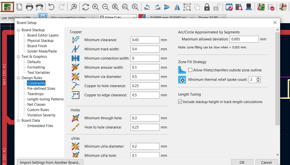
I focused on minimum PCB clearance and minimum trace width because they are essential for PCB functionality and manufacturability.
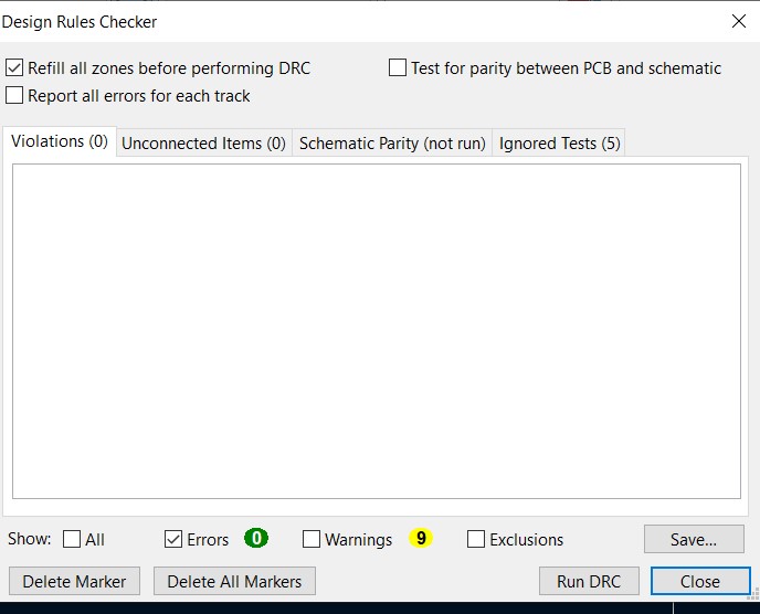
Hopefully, everything is correct and there are no design errors.
4. Notes on the Other Designs I Made
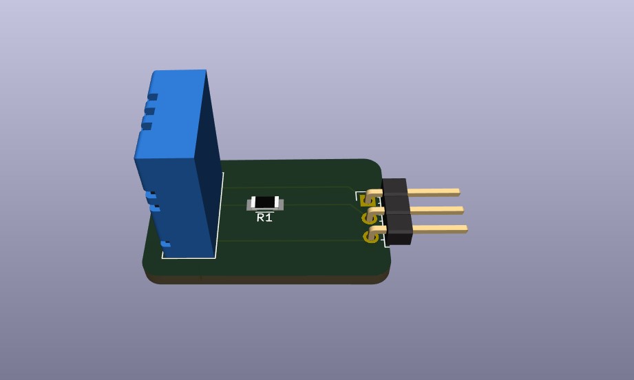
- For the DHT11 PCB design, I followed the same process as the blinking LEDs circuit, but I used different components and connections based on the DHT11 sensor requirements. I used this website as a reference.
- For the final project sample PCB design, I created a more complex design that includes multiple components and connections based on my final project requirements. I also paid more attention to component placement and routing to ensure a compact and efficient design.
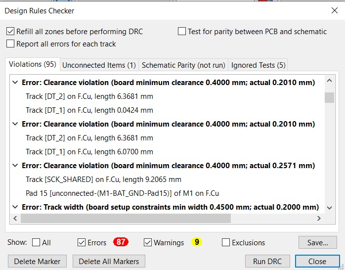 So, I had to fix these errors by editing the line widths for each trace, and believe me, it took a lot of time.
5. Simulation
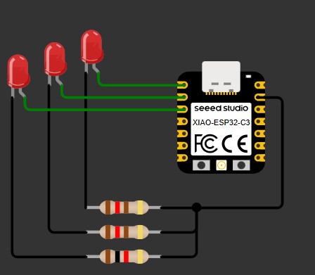
I used Wokwi to simulate the circuit behavior.
- What is Wokwi?
- To create a new project and simulate it, you should sign up on the Wokwi website.
- After signing up, I created a new project by going to my projects on my dashboard and selecting New project.
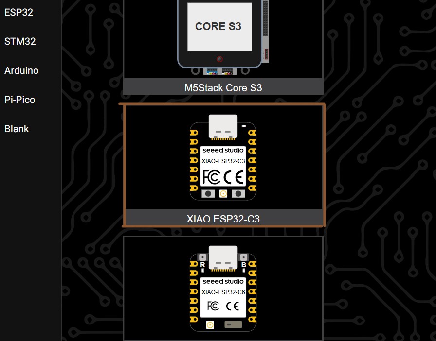
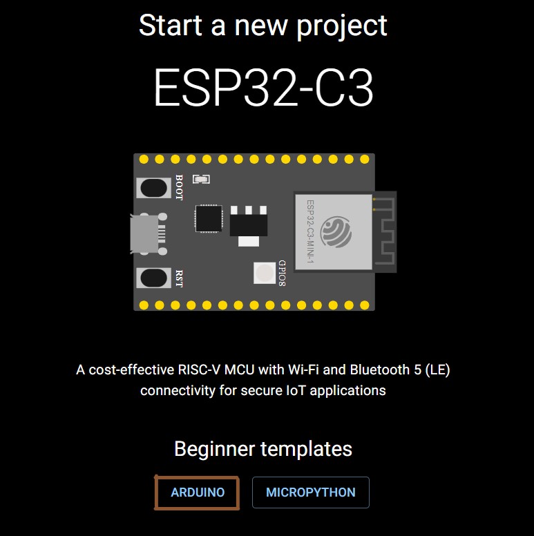
- Then, I selected the same board that I used for the PCB design, which is ESP32-C3.
- After selecting the board, I selected the template and language I wanted to use. Here, I selected ARDUINO because I am familiar with it.
- Now, I have a new project with the selected board and template, and I can start designing my circuit and writing code to simulate it.
- I wrote a simple code snippet for blinking the LEDs, then I ran the simulation to see how it works.
- Then, I could see the simulation results and debug any issues.
Wokwi is an online platform that provides a virtual environment for simulating and prototyping electronic circuits. It allows users to design, test, and debug their circuits using a wide range of components and microcontrollers without the need for physical hardware. Wokwi supports various programming languages and offers features like real-time simulation, code editing, and collaboration tools, making it a valuable resource for students, hobbyists, and professionals in the field of electronics.

      int led1 = D0;
      int led2 = D1;
      int led3 = D2;

      void setup() {
      pinMode(led1, OUTPUT);
      pinMode(led2, OUTPUT);
      pinMode(led3, OUTPUT);
      }

      void loop() {
      // Turn ON LEDs
      digitalWrite(led1, HIGH);
      digitalWrite(led2, HIGH);
      digitalWrite(led3, HIGH);
      delay(500);

      // Turn OFF LEDs
      digitalWrite(led1, LOW);
      digitalWrite(led2, LOW);
      digitalWrite(led3, LOW);
      delay(500);
      }