Week 8: Electronics Production
Group Assignment
For this week's group assignment, we explored our machine specifications and capabilities. We also tried to estimate how much it could cost to produce different PCBs.
You can find the full documentation: Group Assignment Documentation

Individual Assignment
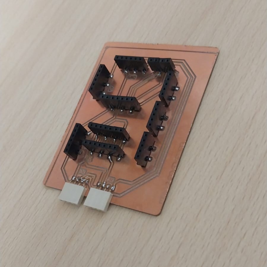
For the individual assignment, I designed and cut a PCB so I could use it for the input and output devices weeks.
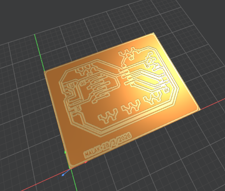
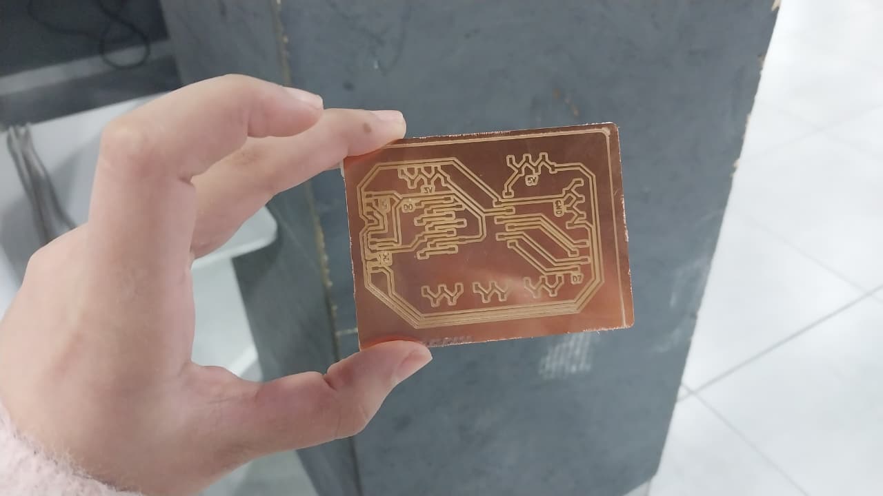
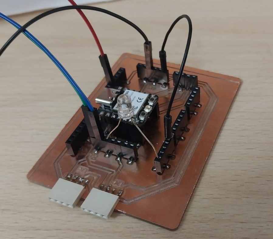
Here is a hero shot of the finished PCB:
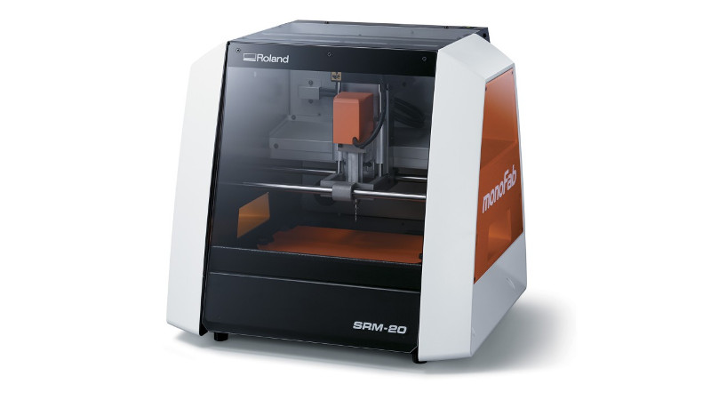
About The Machine
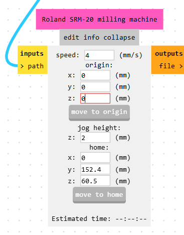
To do My Assignments, I used the Roland SRM-20, as it is the one available in our lab.
Design Process
To design my PCB, I used KiCad software, which I used in the electronics design week and felt comfortable with.
Here are the steps to design the PCB:
- First, I had to check which components were available in the lab so I could design the PCB around them and select the footprints in my design accordingly.
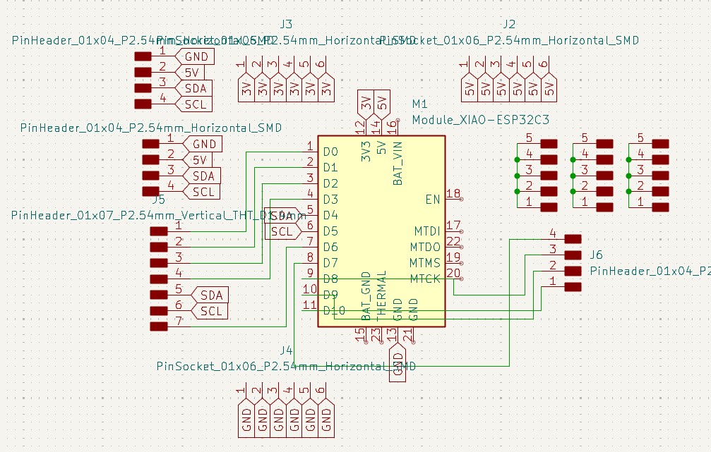
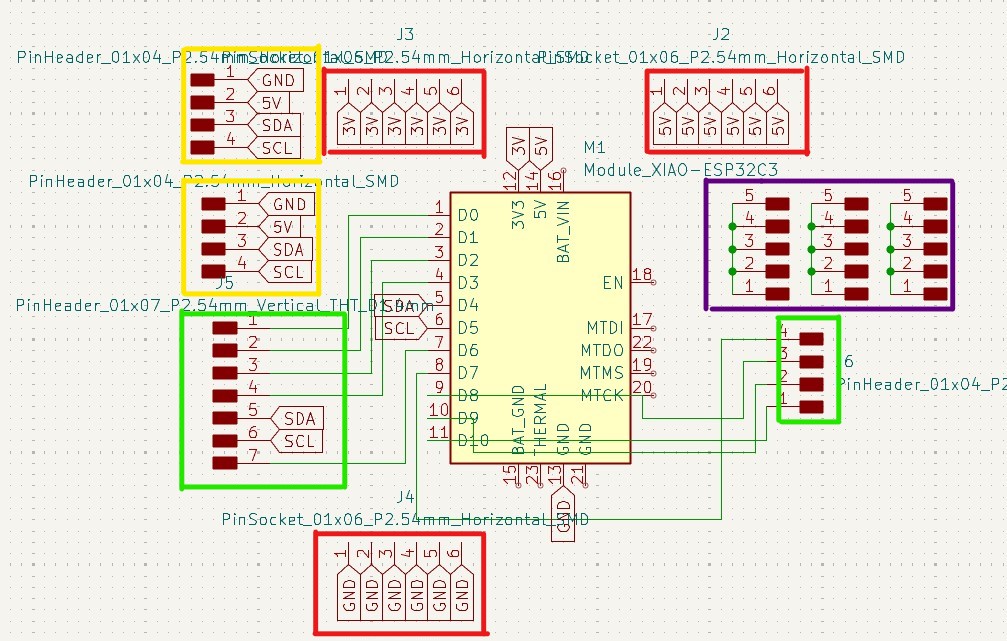
- Then, I created the schematic and layout for the PCB by selecting my components and setting their footprints. Here is the schematic:
- Red Boxes: These represent the source nodes for 5V, 3V, and GND.
- Green Boxes: These represent the input and output pins for the microcontroller.
- Purple Boxes: These represent external nodes that could be used to expand any node in the future.
- Yellow Boxes: These represent I2C connections, so I can connect any I2C device easily.
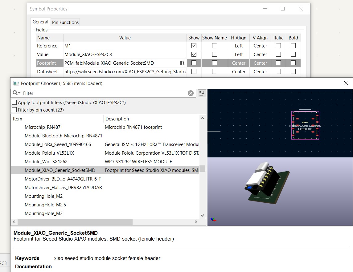
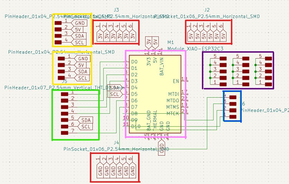
- After that, I selected the footprint for each component. Here are the details for each one:
- Pink Box:
- Value: Module_XIAO-ESP32C3
- Footprint: Module_XIAO-ESP32C3
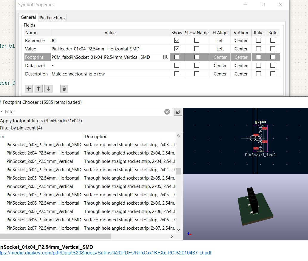
- Blue Box:
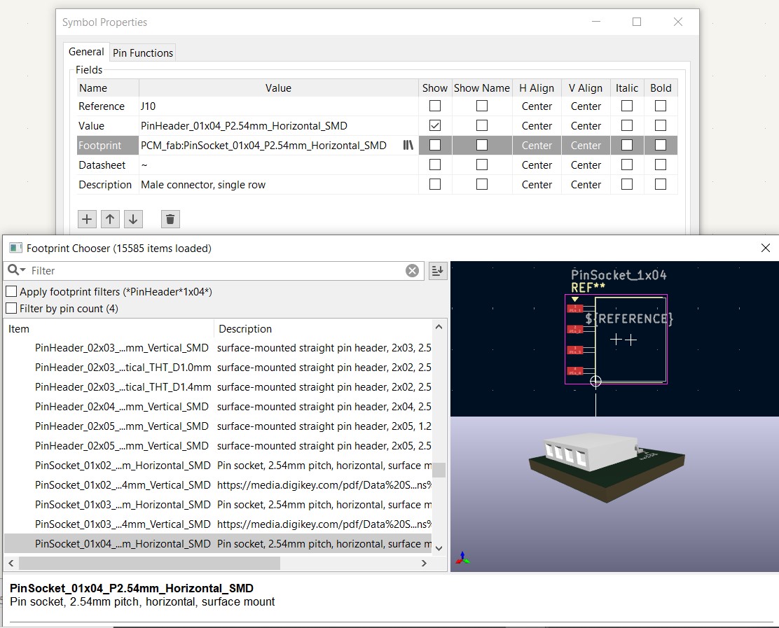
- Value: PinHeader_01x04_P2.54mm_Horizontal_SMD
- Footprint: PCM_fab:PinSocket_01x04_P2.54mm_Vertical_SMD
- Green Box:
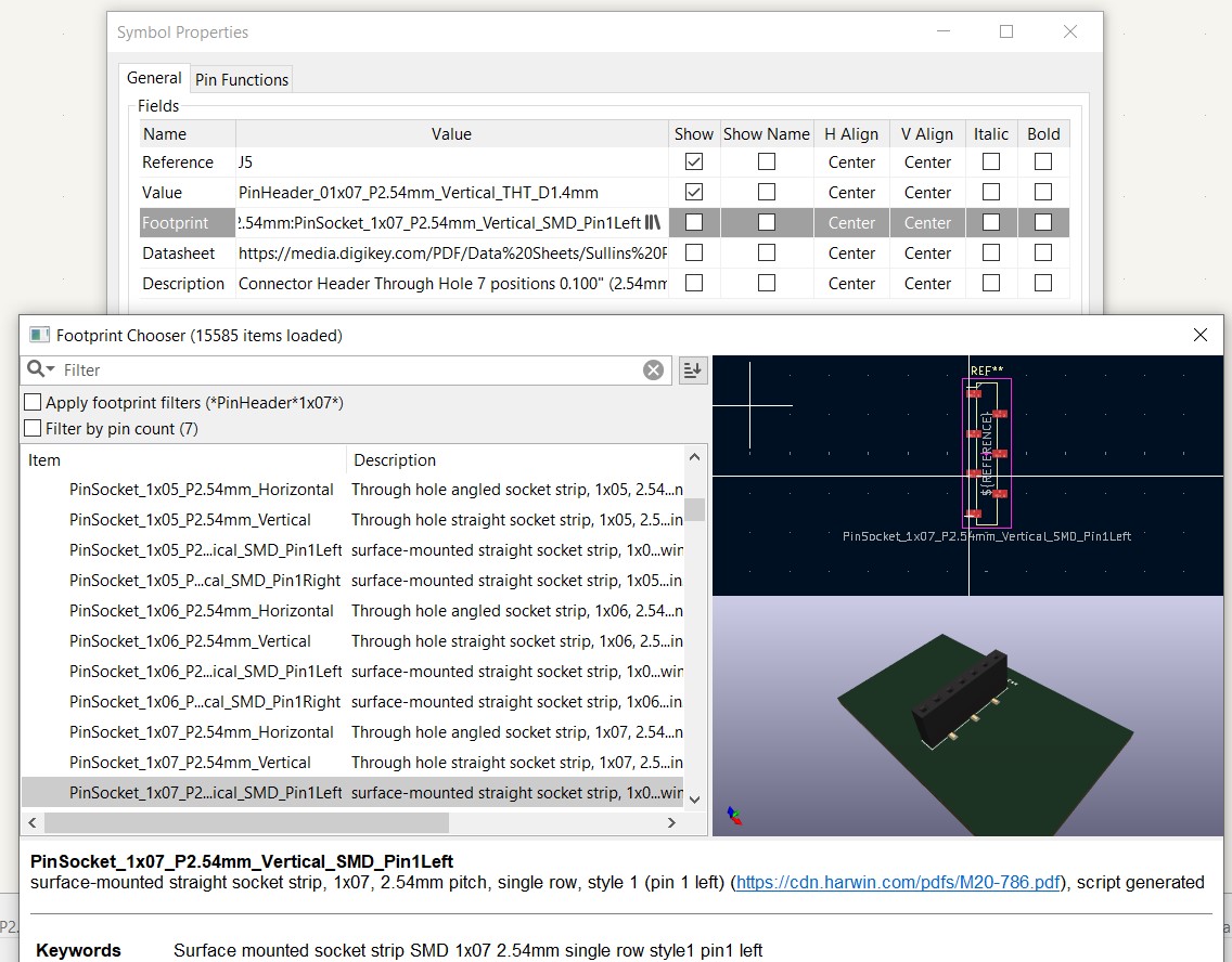
- Value: PinHeader_01x07_P2.54mm_Vertical_THT_D1.4mm
- Footprint: Connector_PinSocket_2.54mm:PinSocket_1x07_P2.54mm_Vertical_SMD_Pin1Left
- Yellow Box:
- Value: PinHeader_01x04_P2.54mm_Horizontal_SMD
- Footprint: PCM_fab:PinSocket_01x04_P2.54mm_Horizontal_SMD
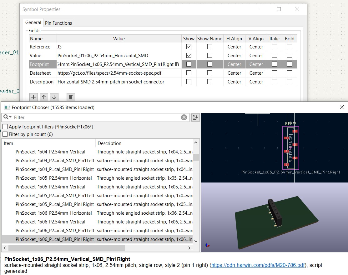
- Red Boxes:
- Value: PinSocket_01x06_P2.54mm_Horizontal_SMD
- Footprint: Connector_PinSocket_2.54mm:PinSocket_1x06_P2.54mm_Vertical_SMD_Pin1Right
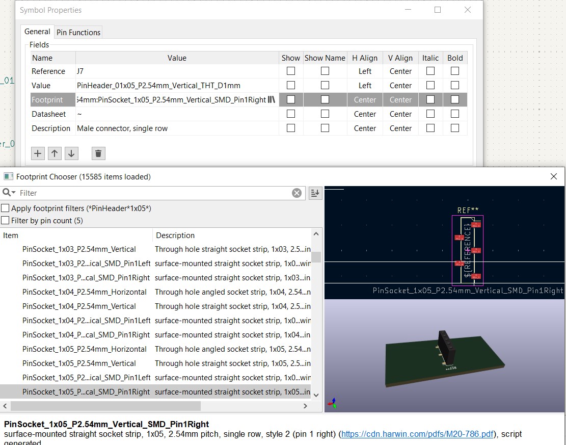
- Purple Box:
- Value: PinHeader_01x05_P2.54mm_Vertical_THT_D1mm
- Footprint: Connector_PinSocket_2.54mm:PinSocket_1x05_P2.54mm_Vertical_SMD_Pin1Right
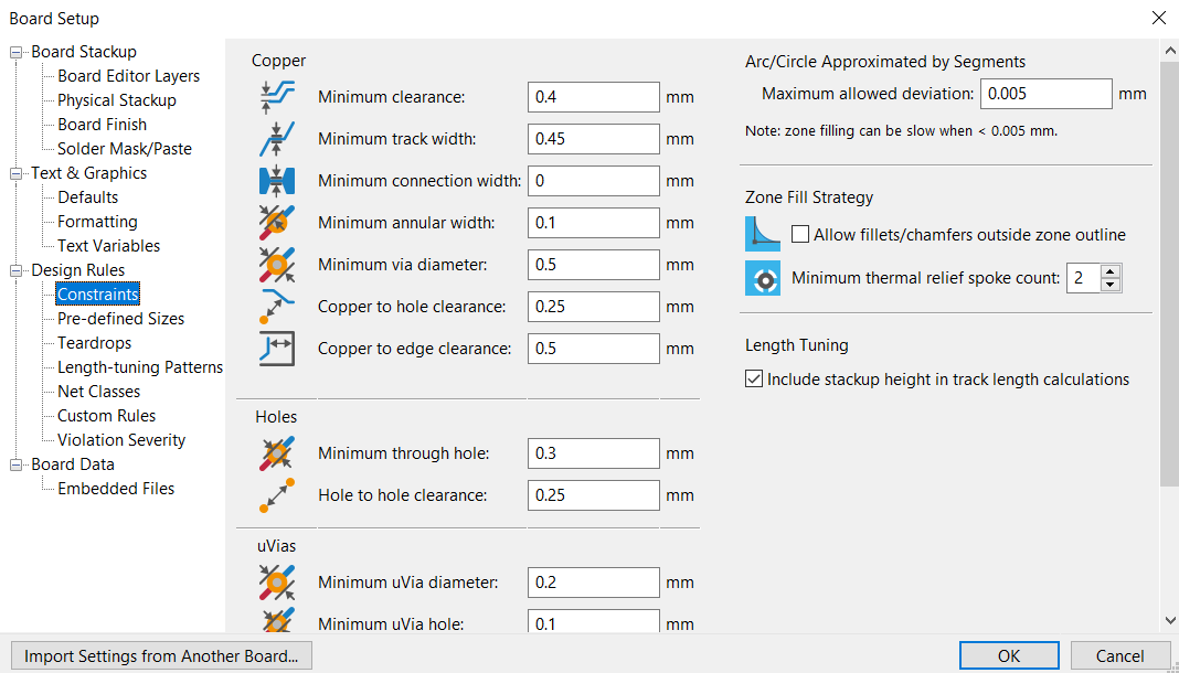
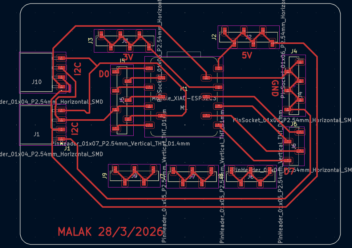
- Then I transferred my schematic to the PCB and set the design rules.
- Next, I routed the connections on the PCB.
- Finally, I ran the design rule checker.
My idea was to create an expansion board for the Xiao Seeed ESP32C3. Here are the details of the design:

Export Files
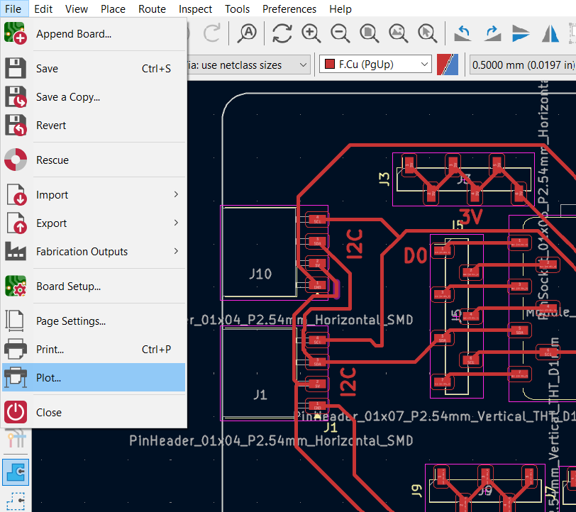
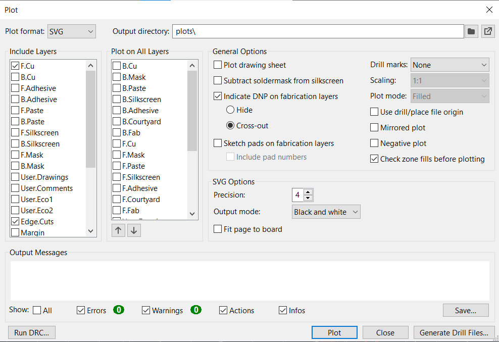
After finishing the design, I exported the cutting files for the CNC machine. Here are the steps:
- Go to the "File" menu and select "Plot"
- In the plot menu, select "SVG" as the plot (output) format, choose the layers you want to export, then click "Plot." In my case, I exported the F.Cu layer for milling and the Edge.Cuts layer for the PCB outline.
You can download the KiCad files and the cutting files for my PCB design: Download PCB Design Files
Prepare files for CNC cutting
After exporting the cutting files, I had to prepare them for cutting on the CNC machine using the MODS website.
Here are the steps to prepare the files for cutting:
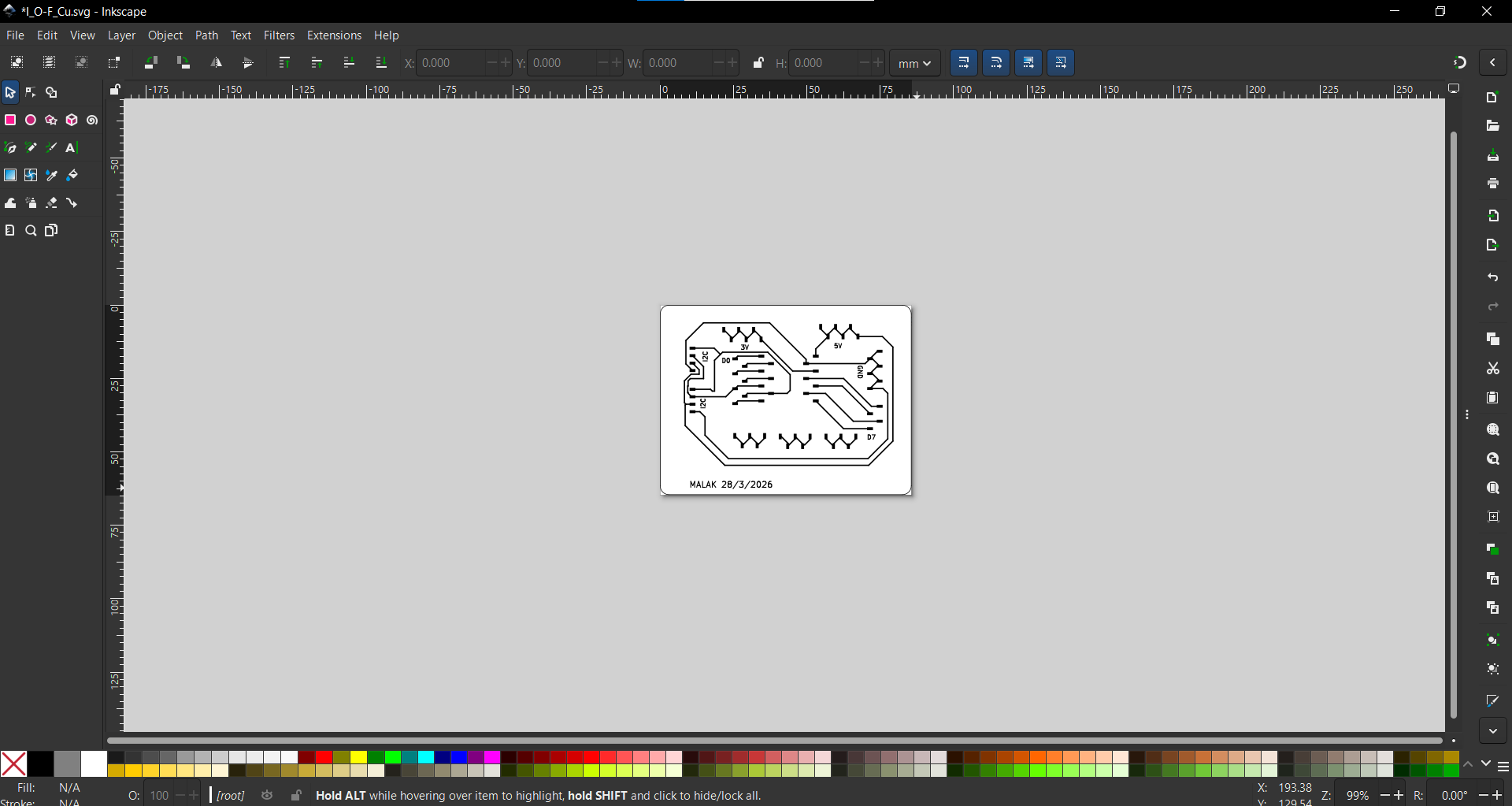
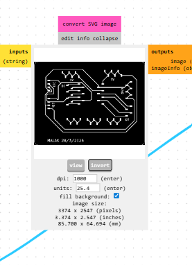
- First, I resized the cutting files in Inkscape by pressing "Ctrl + Shift + R" to set the canvas size to the board size.
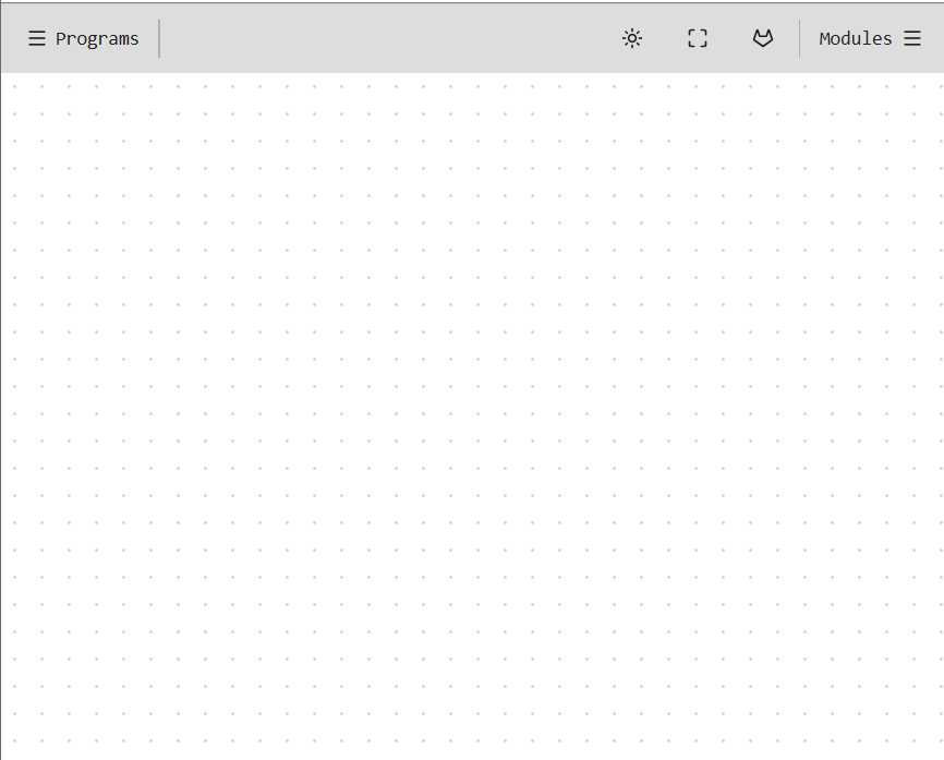
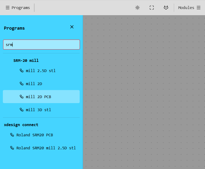
- Then, go back to MODS, open Programs, search for SRM, and select "mill 2D PCB."
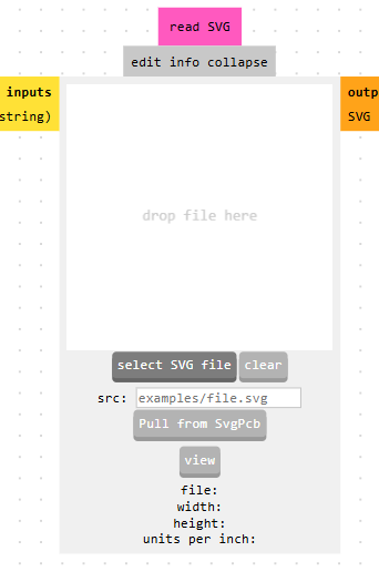
- Next, I uploaded the cutting file for the F.Cu layer by pressing "select SVG file" on "read SVG" block and selecting the correct file.
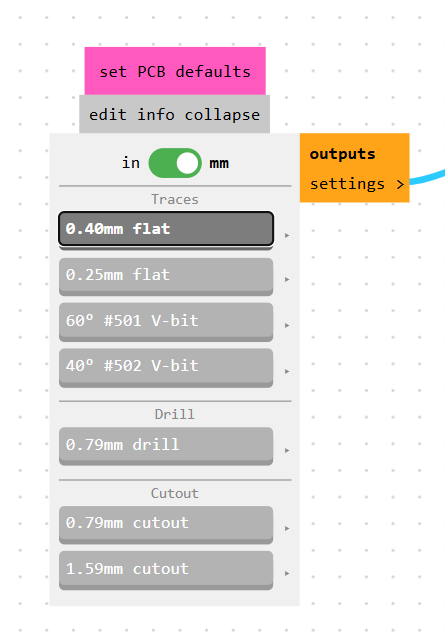
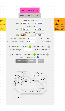
- Select the correct cutting tool. For milling, I used a 0.4 mm tool diameter.
- Check the origin, because by default it is set incorrectly, so reset it to zero.
- Then, press "calculate" in "mill raster 2D" block to generate the cutting paths.
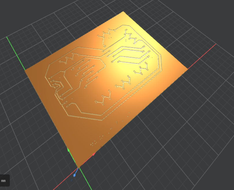
- After that, check the PCB result simulation so you can verify the cutting paths.
- Finally, enable "on/off" block before the save block so when you press recalculate the file downloads automatically.
After that, I had to change some settings such as:
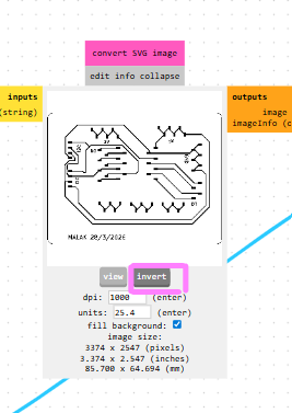
As you can see, this path isn't correct; it is cutting the path instead of what's around it.
To fix this issue, I had to press "invert" in "convert SVG image" block
Now recalculate and see the new simulation.
As you can see, the cutting paths are now correct and it is cutting around the traces instead of cutting the traces.
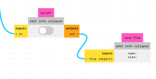
Now you can recalculate and the file will be downloaded automatically.
Redo the same steps for the other layer.
You can download the prepared files for CNC cutting: Download Prepared CNC Files
and here is the Inkscape files: Download Inkscape Files
Machine Setup and Cutting
After preparing the files, I set up the machine for cutting the PCB. Here are the steps:
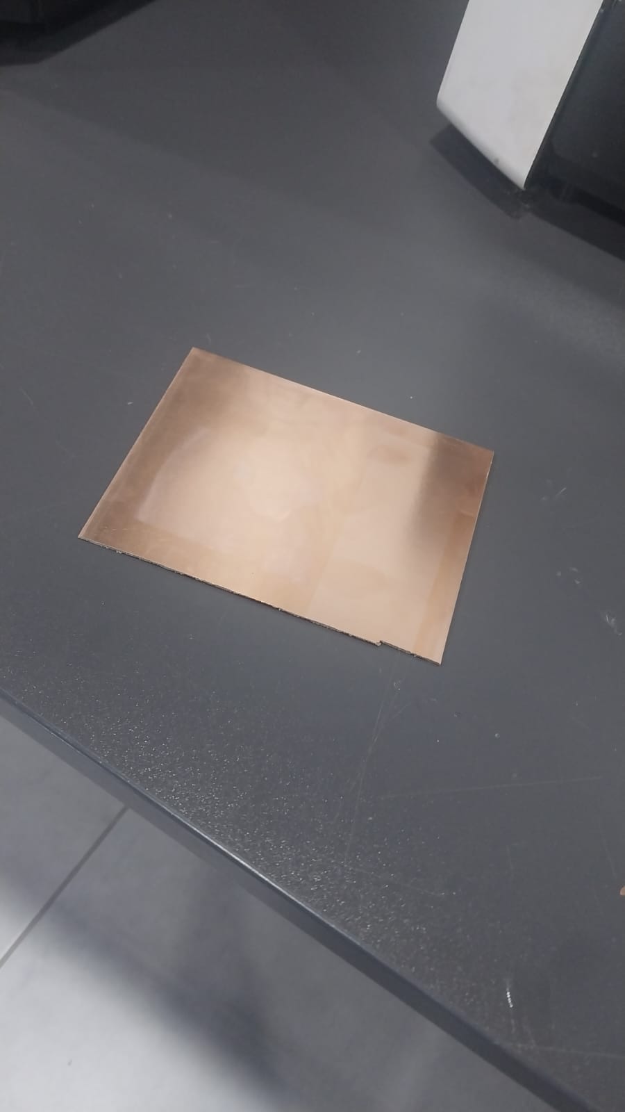
- First I prepared the pcb board since the one we have in our lab is big which make it not 100% flat.
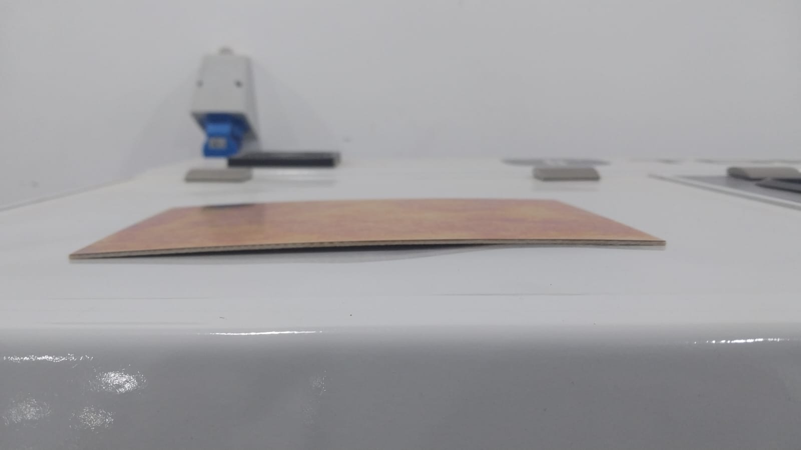
To prepare the board, I had to cut it into smaller pieces that fit the machine and are easier to work with.
So I have now a flat board that make the cutting in all point equal.
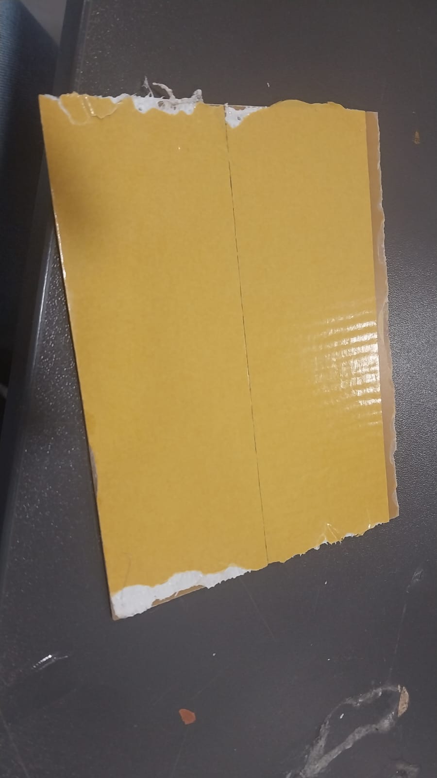
- Then put a double face sticky in the board so we ensure that the board will not move during the cutting process.
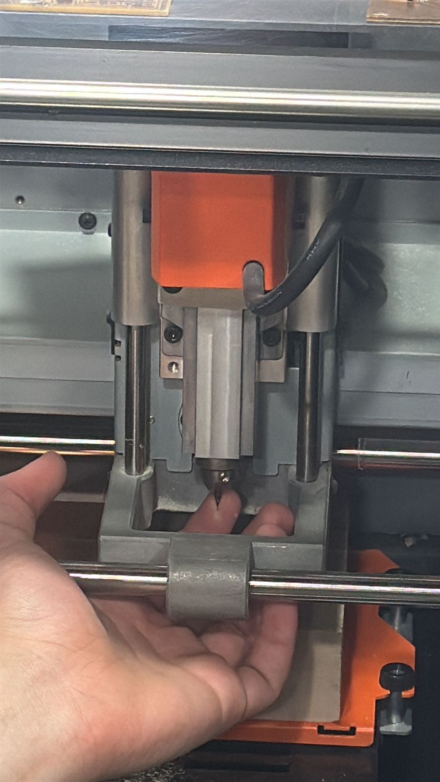
- First, I installed 0.4 mm cutting tool in the machine.
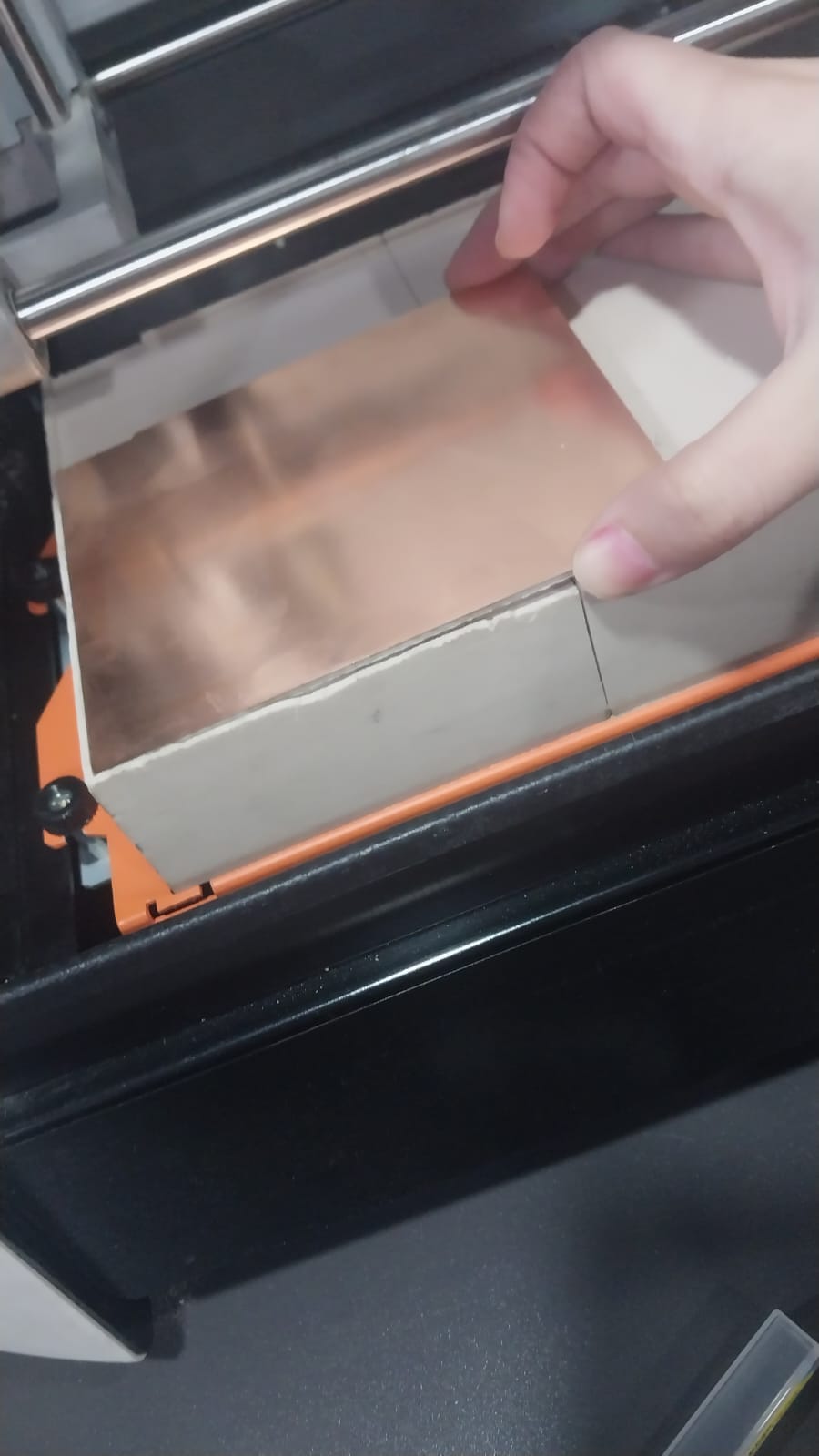
- Then, I set the X and Y axes origin by moving the tool to the top-left corner of the PCB board and setting that position as the origin for both axes.
- Then, I set the Z-axis origin by lowering the tool until it just touches the surface of the PCB board, then set this position as the Z-axis origin.
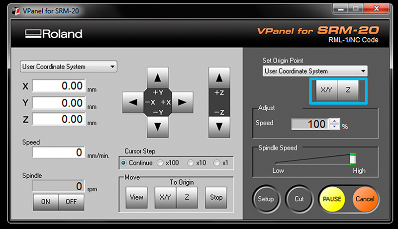
Then, I started the cutting process by running the first file for the F.Cu layer.
Soldering
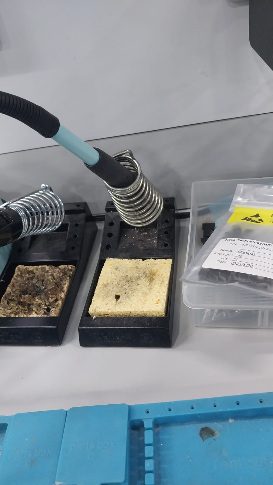
After cutting the PCB, I soldered the components to the board. Here are the steps:
- First, I gathered all the components and tools I needed for soldering, including the soldering iron, solder wire, flux, and the components themselves.
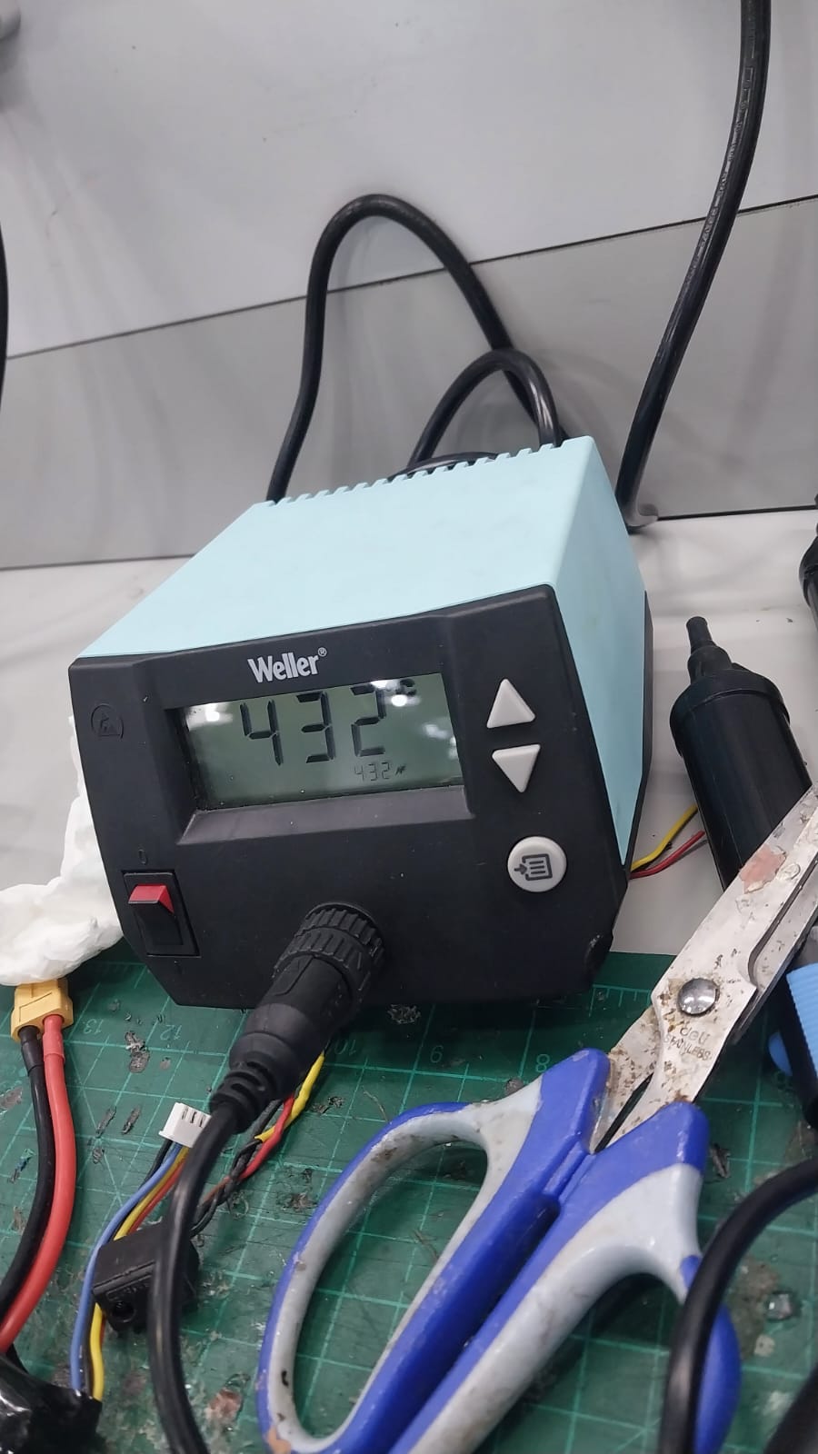
- Then, Started soldering the components to the PCB by following the schematic and layout I designed. I made sure to apply flux to the pads before soldering to ensure good solder joints.
Here is the finished PCB:
Usage Example
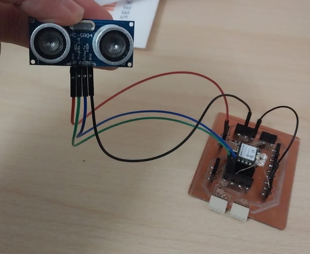
Here is an example of how I can use this PCB to connect a sensor to the Xiao ESP32C3 microcontroller:
Here is the physical connection:
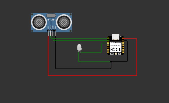
Here is the connection diagram using Wokwi:
Ultrasonic Sensor Code:
Here is the code I used :
// Ultrasonic Sensor Code for Xiao Seeed ESP32-C3
#define TRIG_PIN 2
#define ECHO_PIN 3
#define LED_PIN 4

long duration;
float cm, inches;

void setup() {
  Serial.begin(115200); // ESP32 usually uses higher baud

  pinMode(TRIG_PIN, OUTPUT);
  pinMode(ECHO_PIN, INPUT);
  pinMode(LED_PIN, OUTPUT);
}

void loop() {
  // Clean trigger
  digitalWrite(TRIG_PIN, LOW);
  delayMicroseconds(5);

  // Send pulse
  digitalWrite(TRIG_PIN, HIGH);
  delayMicroseconds(10);
  digitalWrite(TRIG_PIN, LOW);

  // Read echo
  duration = pulseIn(ECHO_PIN, HIGH);

  // Convert to distance
  cm = (duration / 2.0) / 29.1;
  inches = (duration / 2.0) / 74.0;

  // LED control
  if (cm < 18) {
    digitalWrite(LED_PIN, HIGH);
  } else {
    digitalWrite(LED_PIN, LOW);
  }

  // Print
  Serial.print(inches);
  Serial.print(" in, ");
  Serial.print(cm);
  Serial.print(" cm");
  Serial.println();

  delay(250);
}
You could download the full code from here.
Simulation:
Before I upload the code to the board, I simulated the behavior using Wokwi.
You could see the simulation from here.
Connect to the board:
After simulating the code, I uploaded it to the board .