6. Electronics design
Group assignment:
- Use the test equipment in your lab to observe the operation of a microcontroller circuit board (as a minimum, you should demonstrate the use of a logic analyzer)
To see our group assignment click here
Individual assignment:
- Use an EDA tool to design a development board that uses parts from the inventory to interact and communicate with an embedded microcontroller
My individual reflection:
During this group session, we tested the operation of a microcontroller circuit board using four measurement instruments.
With the multimeter connected in parallel across the terminals of a blinking 5mm red LED, we observed a voltage varying between 0 and 2V, corresponding to the alternation between the LED's off and on states (2V being close to its forward threshold voltage).
We then reconnected the multimeter in series with the same LED to measure the current flowing through it, recording a variation between 0 and 12.34 mA, which allowed us to verify that the current stayed within a safe range for a standard LED (typically limited to 20 mA).
On the oscilloscope, we again probed the voltage across the blinking LED, which let us directly visualize the transition between the high and low states over time, unlike the multimeter which only gives a single value or a range.
Finally, using the logic analyzer mounted on the I2C bus between an Arduino Uno and a 0.96" OLED display, we were able to capture and decode the communication frames exchanged between the two components, confirming that the I2C protocol was working correctly.
This exercise helped me concretely understand the difference between the instruments.
Kicad installation
Installing KiCad is fairly straightforward, but depending on your operating system, there are a few specifics you need to know in order to get the most stable version (currently 8.0).
Always visit the official website to avoid outdated versions: 👉 : Kicad
Choose your system:
-
Windows: Download the .exe installer (often via the
GitHublink). -
macOS: Download the
.dmgfile. -
Linux: KiCad is available on almost all distributions (Ubuntu, Fedora, Arch). On Ubuntu, it is recommended to use the official PPA to get version 8.

Adding the “Fab” library (For your project)
-
Download the
kicad-fabfolder from Gitlab Fabcloud. -
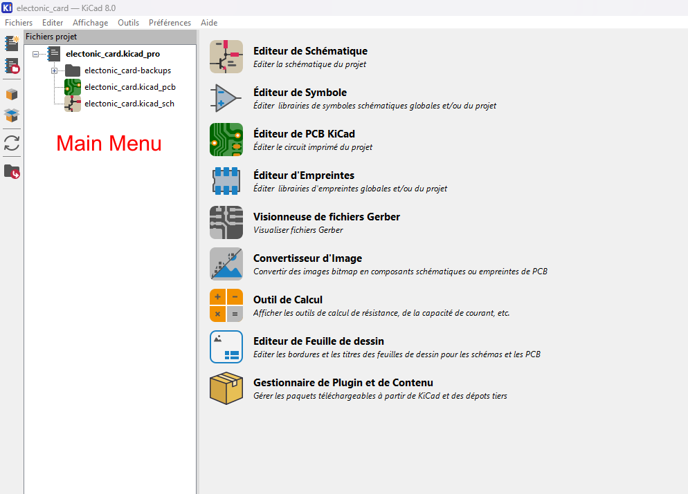
In KiCad (Main Menu):
-
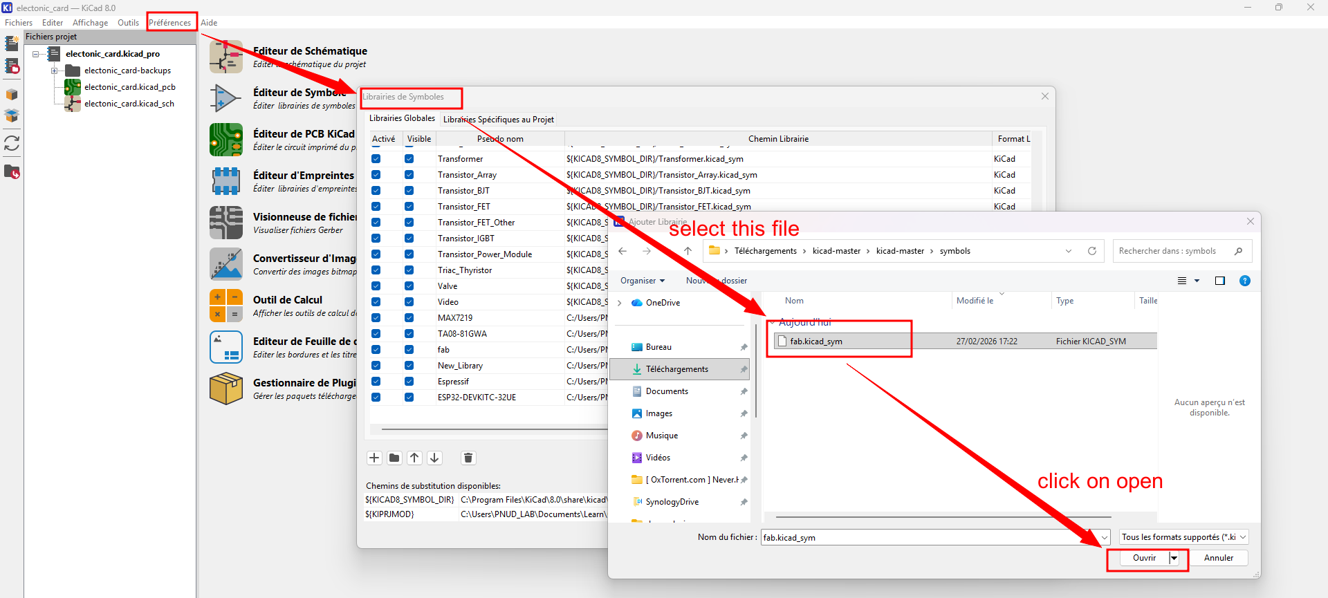
Go to Preferences > Manage Symbol Libraries.
-
Click on the Global Libraries tab.
-
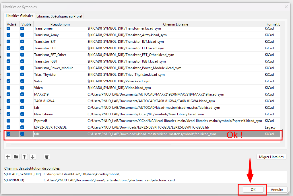
Click on the Folder icon (+) and search for the
fab.kicad_symfile. -
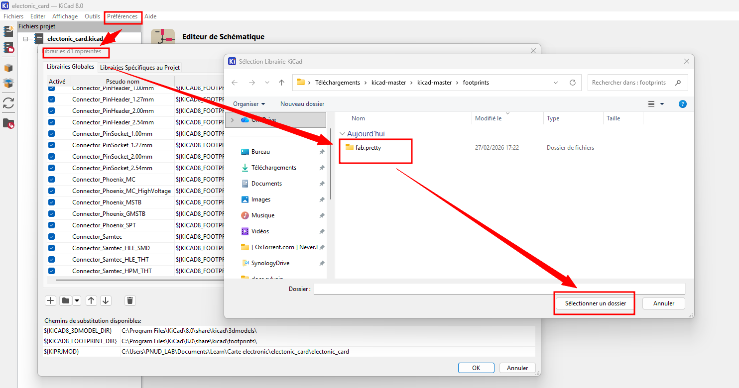
Repeat the same thing in Manage Footprint Libraries for the
fab.prettyfolder.
Design circuit board
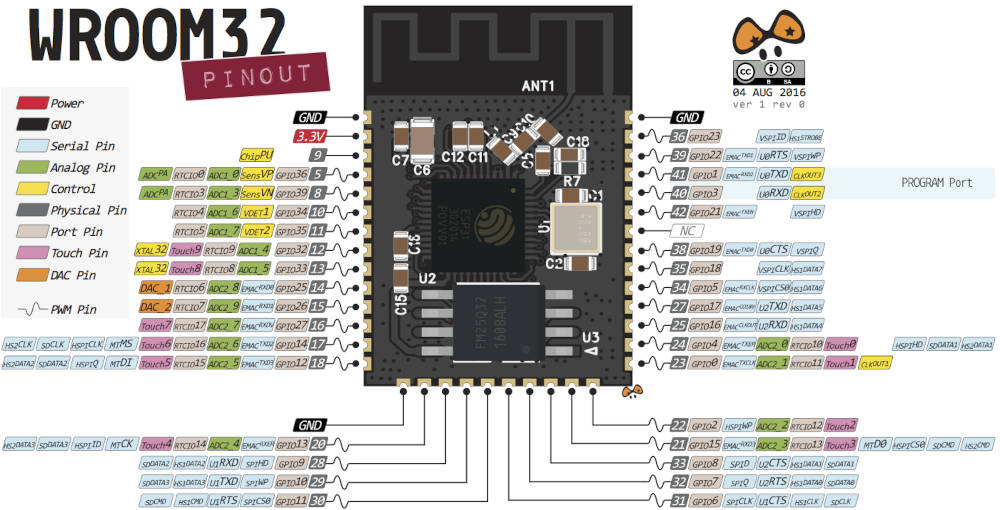
Before beginning the circuit design, we conducted a detailed study of the ESP32 microcontroller to identify the most suitable pins for our project and determine the essential external components required for proper operation.
We first consulted the official ESP32 datasheet, carefully reviewing the description and electrical characteristics of each pin. This analysis enabled us to understand the specific functions, limitations, and multiplexing capabilities of the GPIOs, and to select the terminals that best match our application requirements.
During this review, we also identified an important note in the datasheet regarding certain pins that are not recommended for general use. Recognizing these restrictions early in the design process helped us avoid potential hardware conflicts and ensured a more reliable circuit implementation.
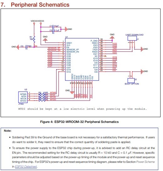
Another key piece of information found in the datasheet is the section titled Peripheral Schematics (Page 19). This section provides essential design recommendations and reference circuits for integrating the ESP32 properly into a hardware system.
Schematic design
This table lists the components used to design our card.
| Reference | Value | Name |
|---|---|---|
| U1 | ESP32-WROOM | ESP-WROOM-32U |
| U2 | Voltage regulator | 3.3 V 100 mA LDO Regulator |
| R1 | 10 kΩ | 10 kΩ NTC Thermistor |
| R2 | 100 Ohm | 100 Ohm Resistor |
| R3 | 100 Ohm | 100 Ohm Resistor |
| R4 | 10 kΩ | 10 kΩ NTC Thermistor |
| R5 | 100 Ohm | 100 Ohm Resistor |
| C1 | 0.1 µF | 0.1 µF Ceramic Capacitor 250 V |
| C2 | 10 µF | 10 µF Ceramic Capacitor 50 V |
| C3 | 10 µF | 10 µF Ceramic Capacitor 50 V |
| LED1 | Transparent Green LED | |
| LED2 | Transparent Green LED | |
| LED3 | Clear Red LED | → Green |
| S1 | Push Button Switch | |
| S2 | Slide Switch | |
| S3 | Push Button Switch | |
| M1 | FTDI SMD Pin Header Connector | SMD CON HEADER |
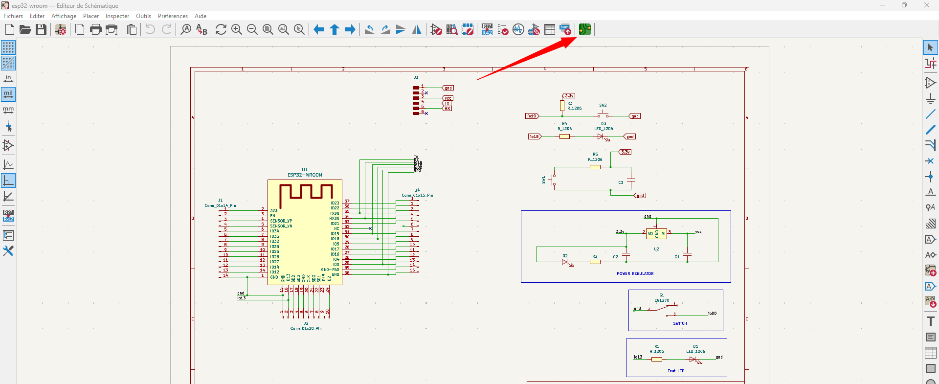
Using the Kicad tool summary table, add the various components to your workspace. Use the Wire and Label tools to achieve the following:
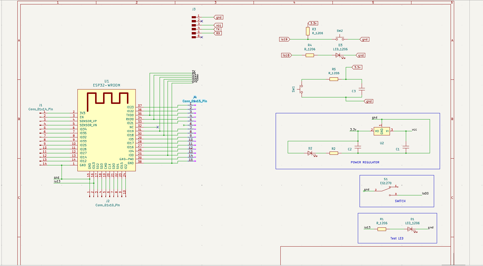
Once your diagram is clean and each symbol is associated with its footprint, save your work.
Circuit simulation
To verify the behavior of the LED + resistor sub-circuit used in the design (LED1/LED2 with their 100 Ω series resistors R2/R3), I simulated it in TinkerCad Circuits. The circuit consists of a 5V DC supply, a 100 Ω resistor, and a red LED in series, with a virtual multimeter measuring the current.
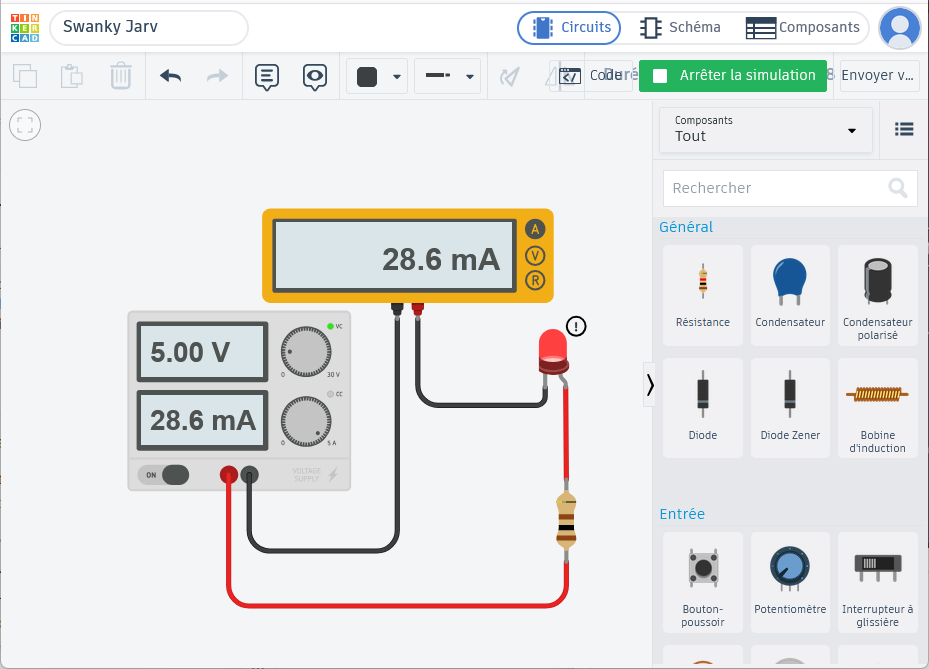
The simulation shows a supply voltage of 5.00V and a current of 28.6 mA flowing through the LED. This corresponds to a calculated LED forward voltage of approximately 2.14V (Vf = 5V − 0.0286A × 100Ω), which is consistent with typical datasheet values for a red LED. The simulation confirms that the 100 Ω resistor value chosen in the schematic keeps the LED current within a safe operating range, validating the resistor sizing used in the design.
Routing design
Click on the symbol indicated by the red arrow to go to the routing area.
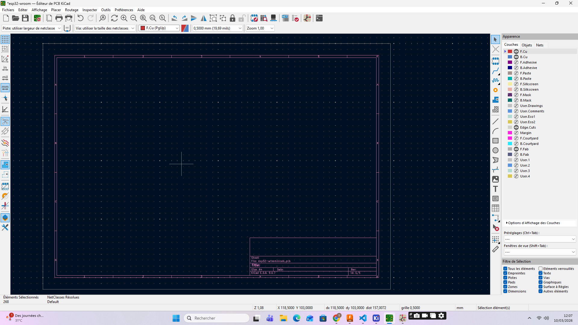
Once in the routing space, KiCad requires the user to perform an update. To do so, do the following:
Click on the symbol indicated by the red arrow to go to the routing area.

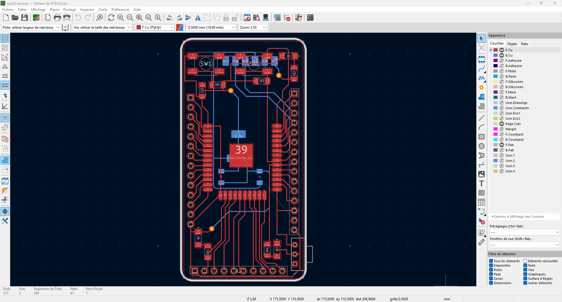
Correction
-
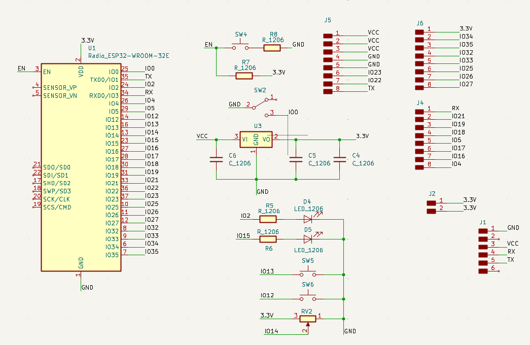
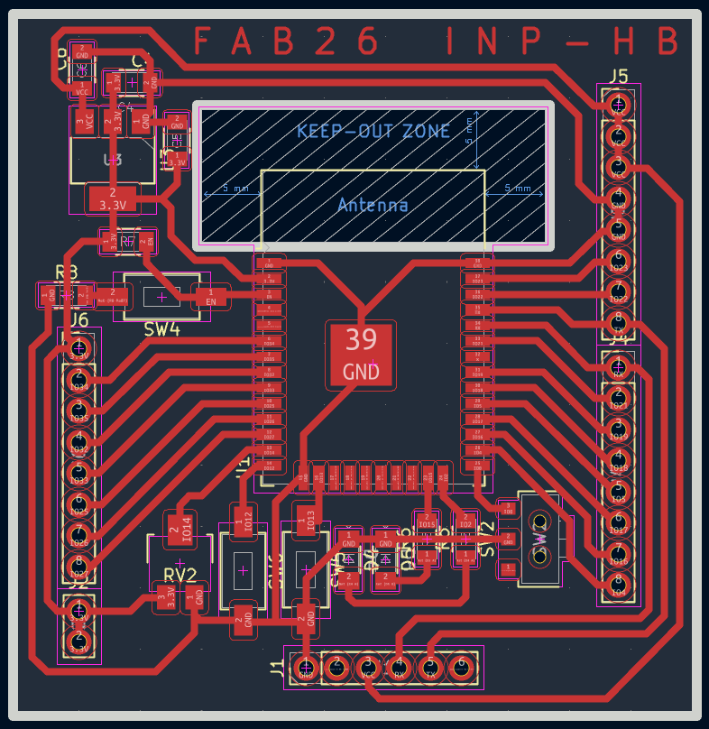
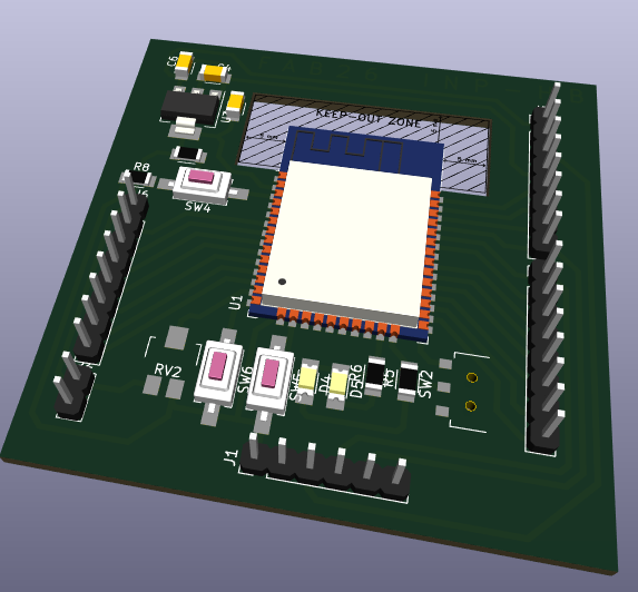
After presenting our work to our local instructor, several issues were pointed out regarding our PCB design, namely:
-
The trace widths
- The component footprints
-
The spacing between traces
-
After applying the various recommendations we were given, we obtained the results shown below.
Design rules verification (ERC / DRC)
ERC result:
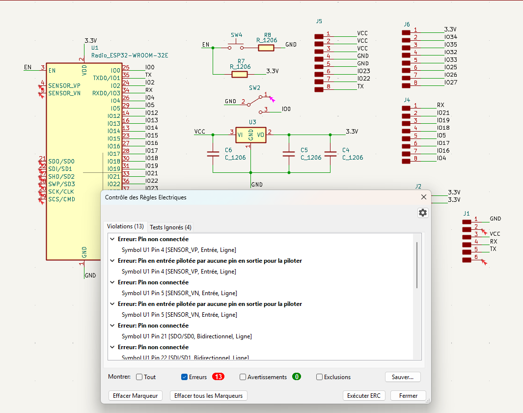
After running the ERC, the only errors reported concerned the pins we deliberately chose to leave unconnected. This confirms that all the other connections in the schematic are properly terminated.
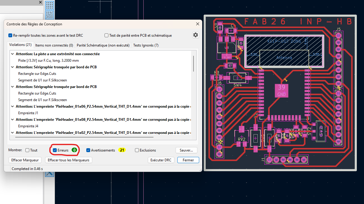
DRC result:
Before running the DRC, we set the track clearance to 0.4mm, since we are using a 1/64" end mill to cut the traces of our circuit. For the holes, we set a minimum diameter of 0.8mm, since we are using a 1/32" tool.
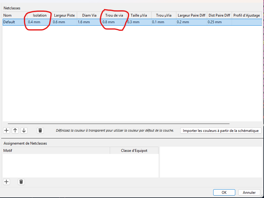
Here is the DRC result: all the remaining warnings are related to the silkscreen positioning of the different footprints, which has no effect on the manufacturability of our circuit.
SVG files generation
To generate the SVG files, click on the Plot tool and select the options as shown in the image below.
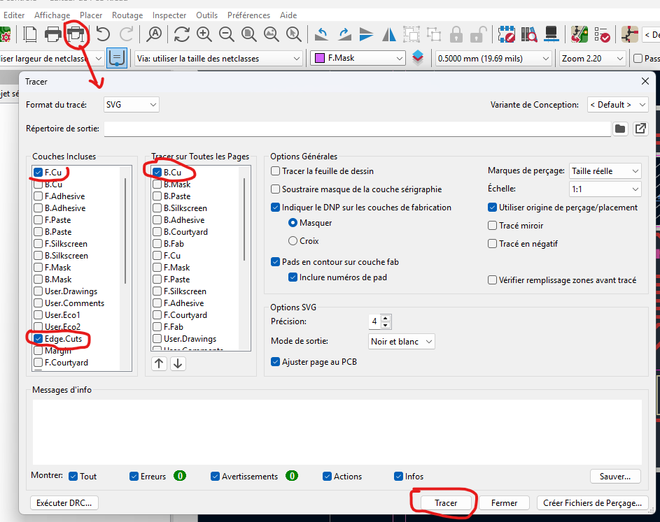
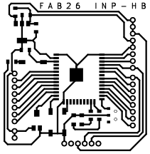
Here are the results:
- Traces
- Holes
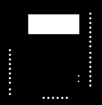
- Outline

Warning
All the SVG files generated above (traces, holes, outline) will undergo a color inversion before generating the toolpaths for milling. This step is necessary because the isolation routing process requires the milling tool to remove the copper around the traces rather than the traces themselves — so the black/white areas of the exported SVG need to be swapped to correctly define what the mill should cut.