Week 8: Electronics Production
Week 8 Assignment:
-
Group Assignment
- Characterize the design rules for your in-house PCB production process
- Submit a PCB design to a board house
-
Individual Assignment
- Make and test an embedded microcontroller system that you designed
-
Extra credits:
- Make it with another process
Notes from the Lecture
-
Design rules: what is the actual spacing, how close can it be together. and how skinny can you make a trace and it still survive.
-
end mill
- material
- fixturing -> to hold the position. one way to do it is with tape underneath, another way is with clamps. with clamps -> make sure it doesn’t bow/no bending -> stress the board and can break end mills. MAKE SURE THE BOARD STAY FLAT
top to bottom
- materials
- underlay -> sacrifical layer. it must be flat, or else it will be a problem: your board won't be uniform. you periodically need to replace the underlay.
- moving bed
PCB Materials
- FR4 -> a glass fiber in epoxy metrics. this is hazardous for machining, we don't do it inside the labs
- FR1 -> copper with phenolic materials, safe and no hazard
- garolite
- copper -> usually we use 1.0 oz: 35 um
GROUP ASSIGNMENT
Chai Huo Week 8 - Group Assignment
PCB Production
(18 March 2026) This week, I explored different ways to produce a PCB. While waiting for the new CNC milling machine to arrive, I tried vinyl cutting, but it did not turn out as planned…
CNC Milling
(18 March 2026) The CNC milling machine is not working, so we are still waiting the new one to arrive.
(22 March 2026) The new CNC milling just arrived, but not yet set up.
(April 2026) Tried the CNC milling!
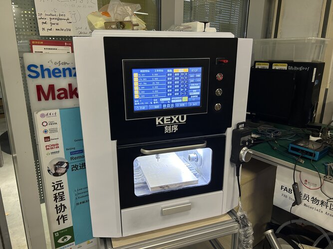
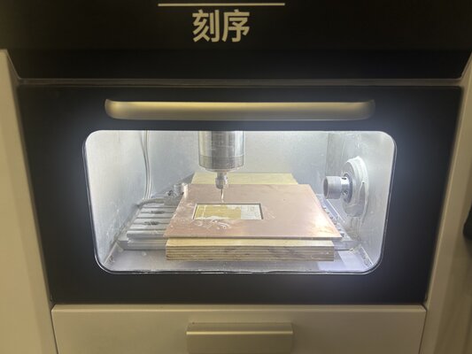
CNC Milling Machine - KEXU (刻序)
KEXU (刻序) CNC machine, likely used for precision modeling or prototyping.
- Features a touchscreen interface for control and monitoring
- Includes a small enclosed working chamber with internal lighting
- Equipped with a physical controller for manual adjustments
- Commonly used in industrial or educational makerspaces for engraving materials
Specifications:
- Working area: 190 mm (X) × 120 mm (Y) × 110 mm (Z)
- Spindle speed: 0–24,000 RPM
- Supported tool diameter: 1–6 mm
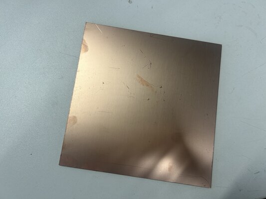
Copper FR4
Copper-clad FR4 is a widely used material for printed circuit board (PCB) fabrication.
Properties:
- Substrate: FR4 (a glass-reinforced epoxy laminate known for its strength, electrical insulation, and flame resistance)
- Copper layer: Single-sided (copper is laminated on one side only)
- Board thickness: 1.5 mm (standard thickness for many PCB applications)
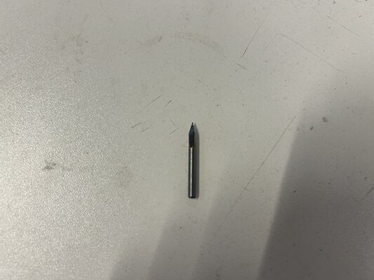
Milling Bit
40° V-bit
- Used for engraving fine PCB traces and cutting board edges
- The sharp angle allows for precise detail and narrow trace isolation
- Suitable for shallow cuts and high-precision milling tasks
CNC Milling Safety
- Wear eye protection and a mask – FR4 dust (fiberglass) is harmful to inhale and can irritate skin and eyes
- Secure the PCB firmly before milling to prevent movement or tool breakage
- Keep hands away from the spindle while the machine is running
- Ensure proper ventilation or dust extraction when milling FR4
Make Your Own Development Board
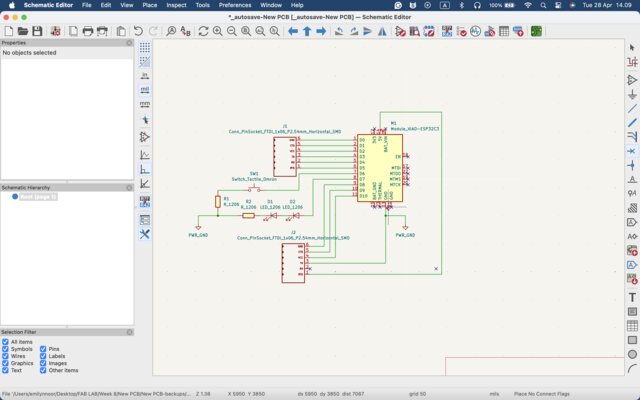
I used KiCad to design both the schematic and the PCB layout for this project.
-
I started by creating a new project on Schematic Editor.
-
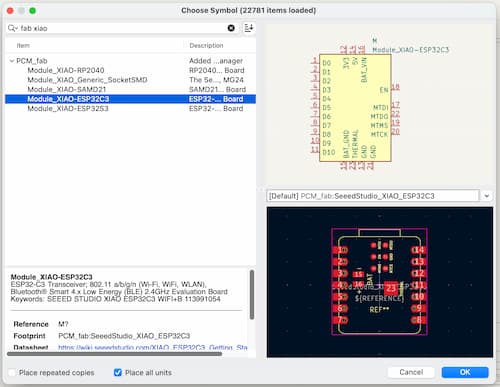
Press
Place->Place Symbols. Then, I used the KiCad FabLib plugin to add the components from the inventory to the schematic and arrange them.-
XIAO ESP32-C3 (microcontroller)
-
Buttons
Switch_Tactile_Omron(input component)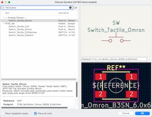
-
LEDs
LED_1206(output component)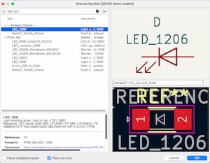
-
Resistors
R_1206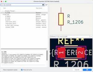
-
Ground
PWR_GND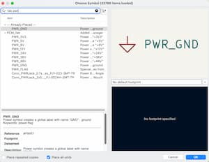
-
Pin Socket
Conn_PinSocket_FL_1x06_P2.54mm_ HorizontaL_SMD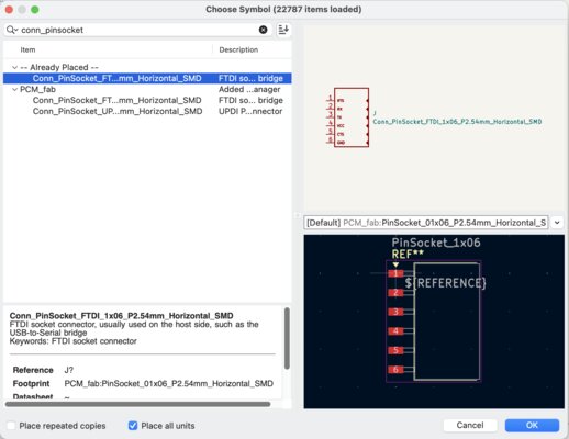
Why use Pin Sockets?
Pin sockets are essential for development boards because they provide modularity. They allow you to easily connect and disconnect different input/output components using jumper wires without the need for permanent soldering. This makes the board reusable for various projects, easy to prototype with, and simple to troubleshoot.
The component assemblies are shown below:
-
-
After wiring the components according to my circuit design, I ran the Electrical Rules Checker (ERC) to ensure there were no logical errors or disconnected pins.
-
Click
Inspect->Electrical Rules Checker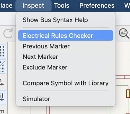
-
Click
Run ERC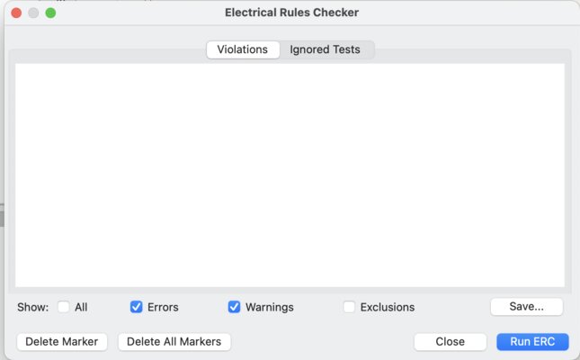
Found 2 Warnings
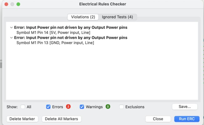
The checker flagged two warnings. After reviewing the connection, I determined it was a non-critical power flag issue and chose to ignore it, as the circuit logic is functional.
-
-
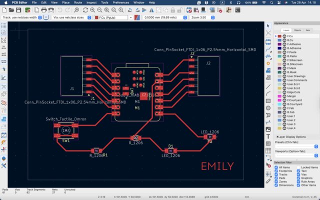
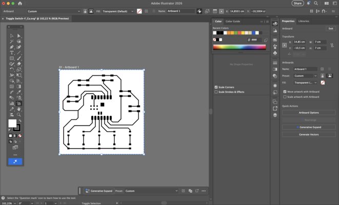
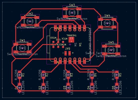
Once the schematic was finalized, I transferred the design to the PCB Editor. I arranged the components to minimize trace lengths and ensure a compact footprint.
Prepare the G-Code Files
-
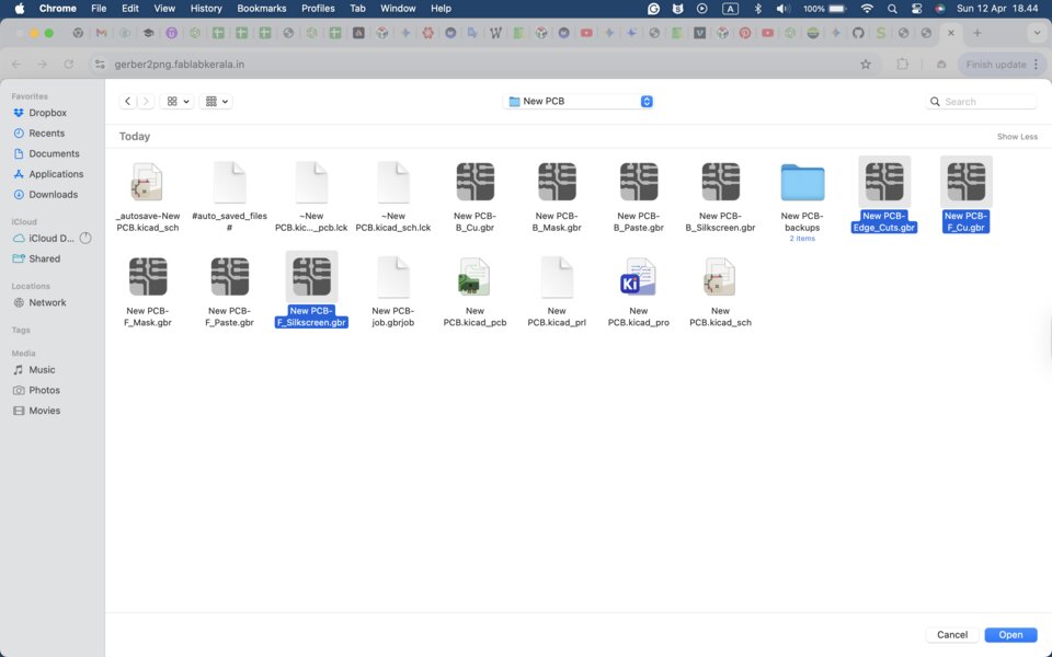
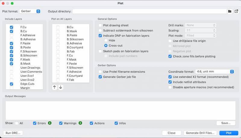
Firstly, we need to prepare the Gerber files from KiCad.
Go to File -> Fabrication Outputs -> Gerbers (.gbr)
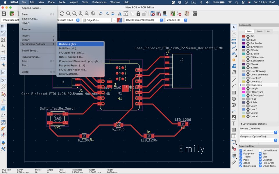
Then select the layers that you want to export.
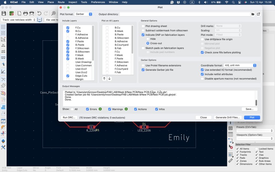
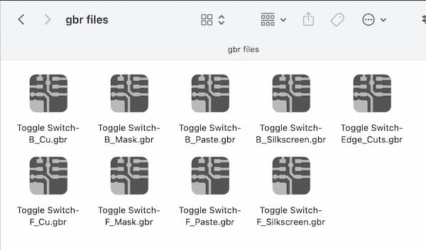
After that, the Gerber files will appear in the designated folder like this:
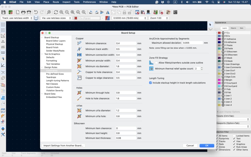
Design Rules
This shows the design rules for my board that worked well with CNC milling.
-
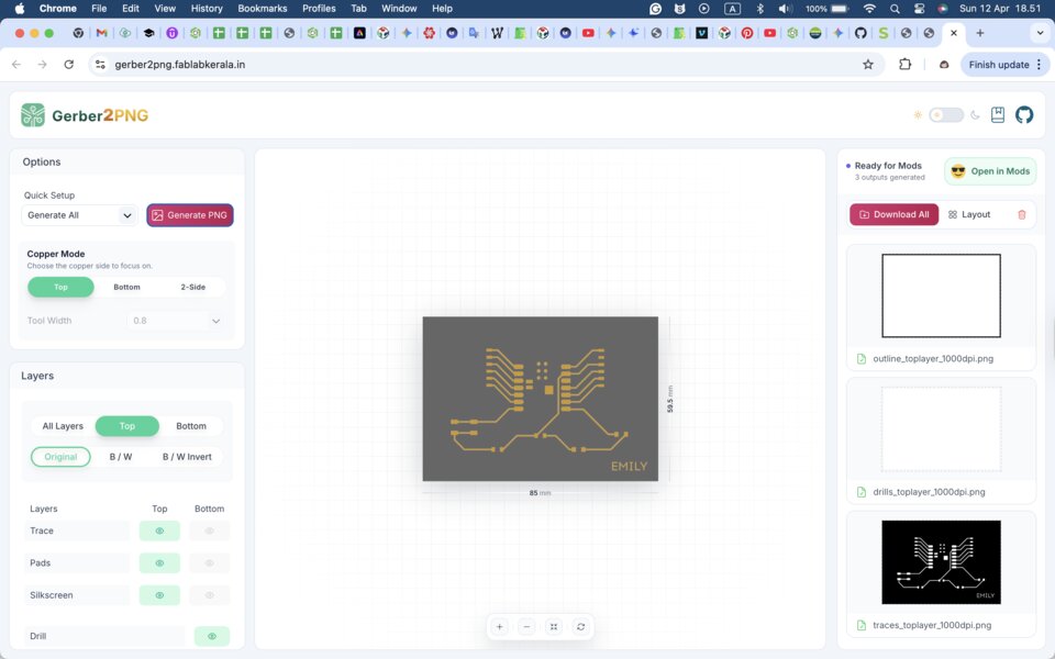
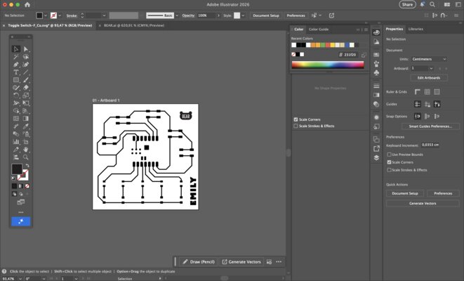
Next, convert the Gerber files to PNG files using gerber2png.
Open the website in your browser:
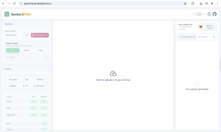
Upload the Gerber files:
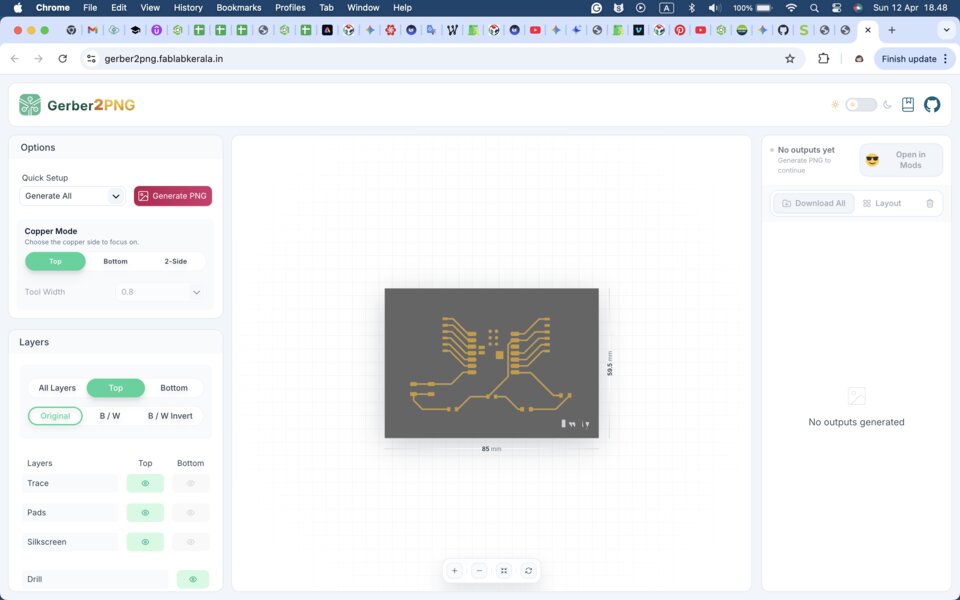
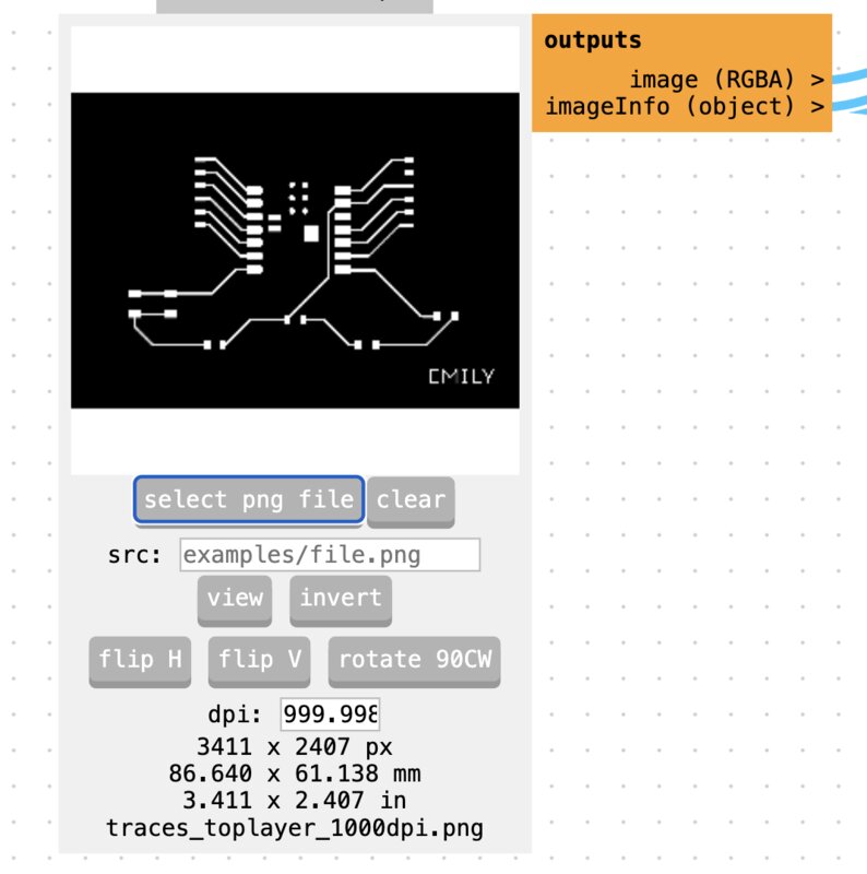
The output files will appear on the right side of the screen. Download them. I downloaded two files:
outline.pngandtraces.pngIf the trace file is correct, the traces should appear white, and the background should be black, like this:
-
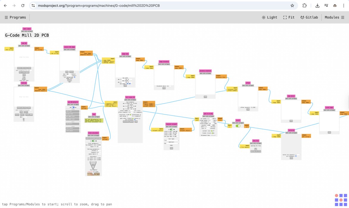
Next, convert the PNG files to G-code using Mods Project. I used both outline.png and traces.png as input for Mods.
Open the Mods Project website:
-
TRACES
-
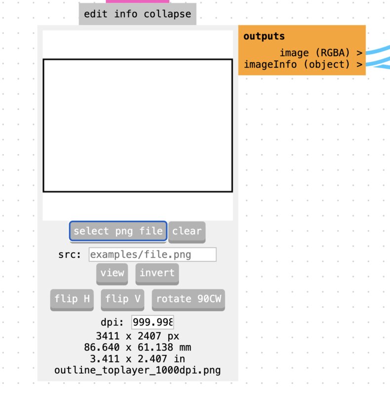
This tool works with both SVG (top section) and PNG (bottom section). I used PNG. Click “select png file”
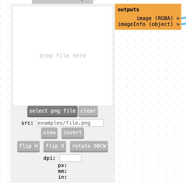
-
Select your traces.png file:
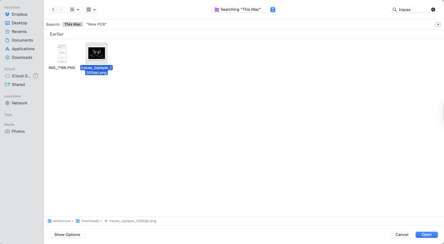
It will appear in the preview like this:
-
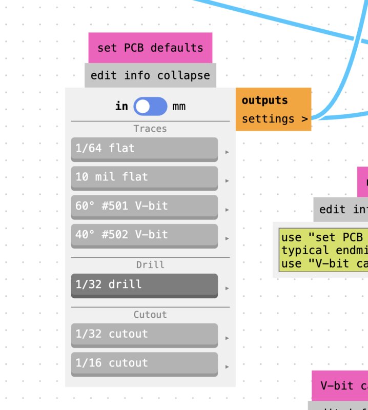
Set the PCB milling preset:
Choose “40°#502 V-bit”
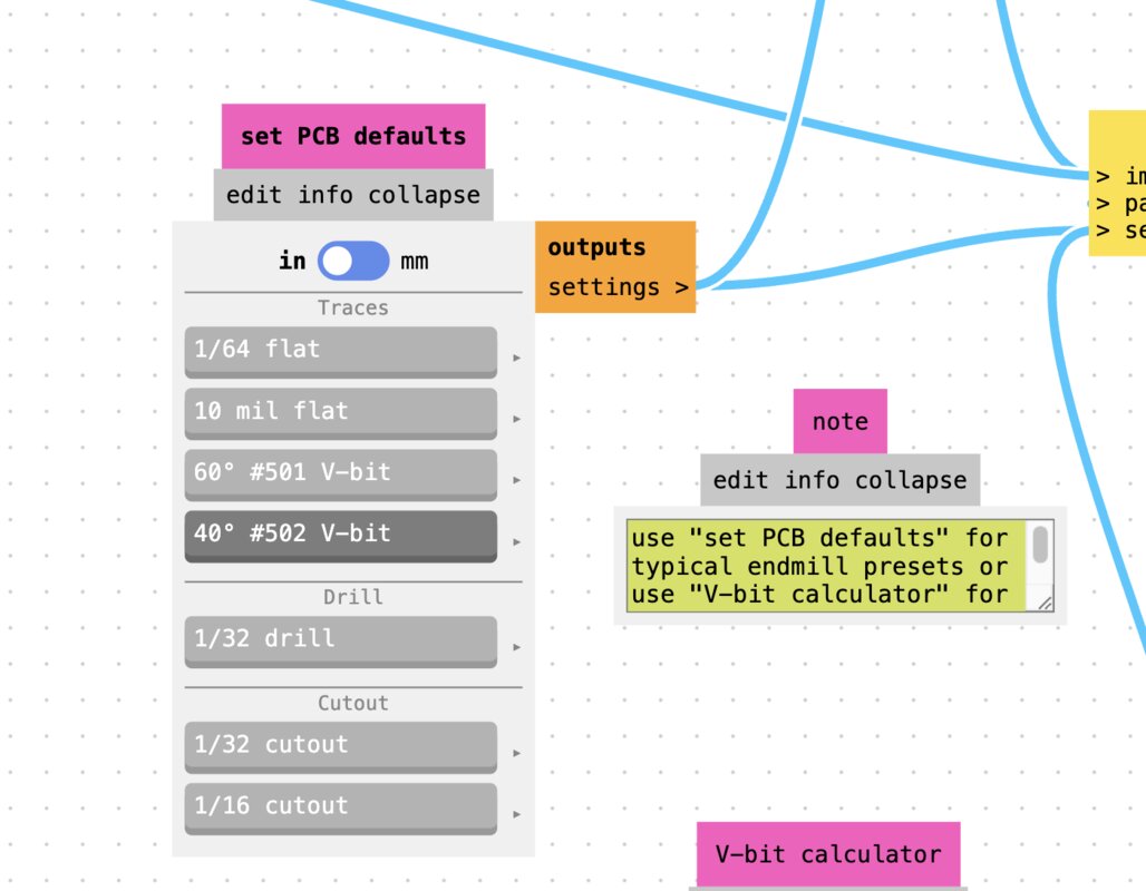
PCB Milling Presets
Includes presets for traces (1/64, 10 mil, 60° and 40° V-bits), drill (1/32), and cutout (1/32, 1/16), with in/mm toggle.
-
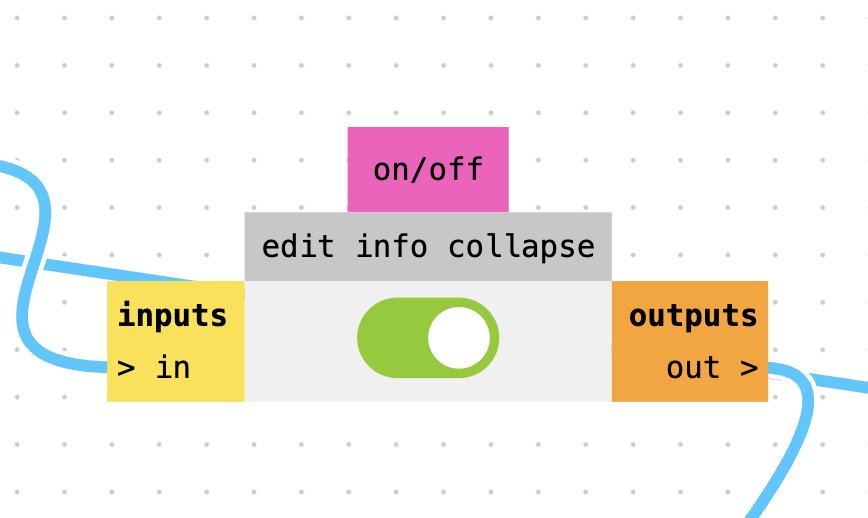
Enable file output by turning ON the toggle.
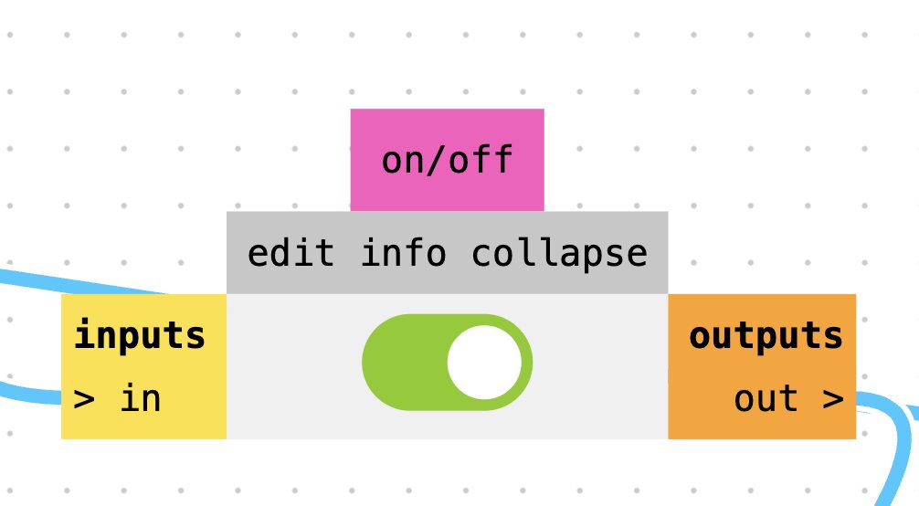
On/Off Toggle
When ON, the signal passes through to output. When OFF, it is blocked.
-
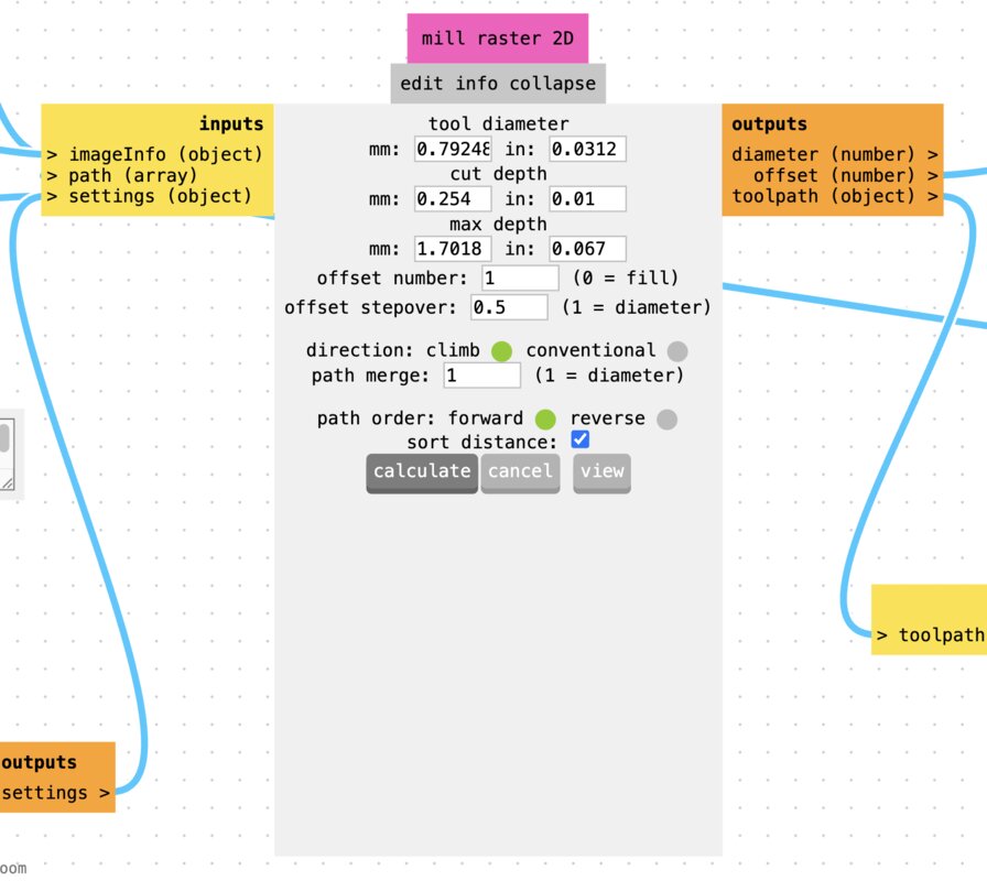
In Mill Raster 2D, click “calculate” to generate the G-code.
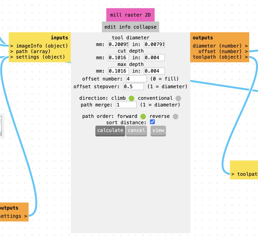
Mill Raster 2D
Configures parameters like tool diameter, cut depth, offsets, stepover, direction, and path sorting.
-
A 3D preview will be shown:
-
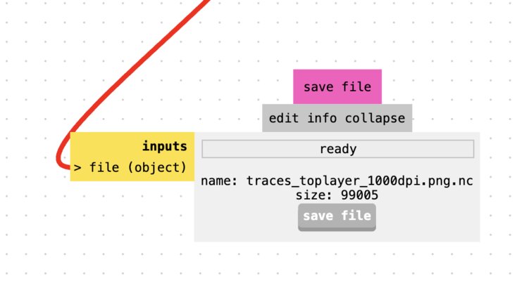
Click “save file” to download the G-code.
-
-
OUTLINE
-
Click “select png file”
 -
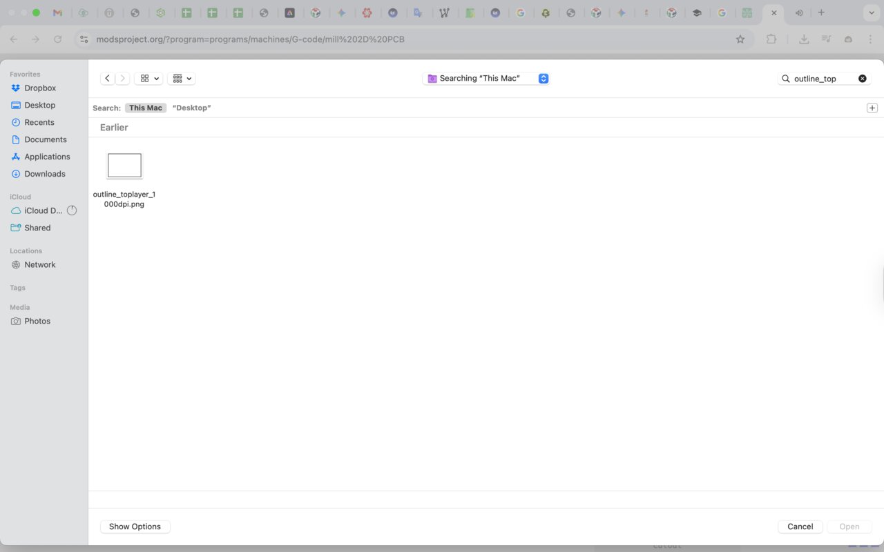
Select your outline.png file:
Preview:
-
Set the PCB milling preset:
Choose “1/32 drill”
-
Turn ON the output toggle:
-
Click “calculate” in Mill Raster 2D:
-
Save the file.
-
-
-
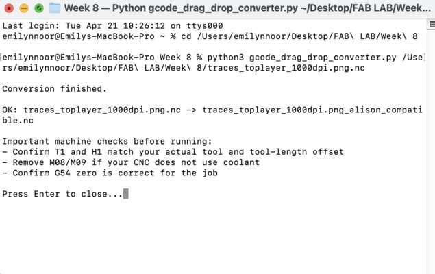
Convert the generated G-code to a machine-compatible format.
Our instructor, Matthew, provided a Python script for this.
#!/usr/bin/env python3
from pathlib import Path
import re
import sys

STARTUP_PATTERNS = [
    r'^G17$', r'^G21$', r'^G40$', r'^G49$', r'^G54$', r'^G80$', r'^G90$', r'^G94$',
    r'^G98$', r'^F[-+]?\d', r'^S[-+]?\d', r'^M0?3$', r'^G0?0Z'
]

def convert_file(src_path: Path, program_number: int) -> Path:
    lines = src_path.read_text(errors='replace').splitlines()
    clean = [ln.strip() for ln in lines if ln.strip() and ln.strip() != '%']

    body = []
    started = False
    for ln in clean:
        if not started and any(re.match(p, ln, re.I) for p in STARTUP_PATTERNS):
            continue
        started = True
        body.append(ln)

    while body and re.match(r'^(M0?5|M30|%)$', body[-1], re.I):
        body.pop()
    while body and re.match(r'^G0?0X0+\.?0*Y0+\.?0*(Z20(?:\.0*)?)?$', body[-1], re.I):
        body.pop()
    while body and re.match(r'^G0?0Z(2|5|20)(?:\.0*)?$', body[-1], re.I):
        body.pop()

    adapted = [
        '%',
        f'O{program_number:04d}',
        '(ADAPTED FOR ALISON2026-STYLE CNC STARTUP)',
        'G90 G40 G49 G80 G94',
        'G21 G17 G54',
        'T1 M6',
        'S11000 M03',
        'G00 G90 X0.0000 Y0.0000 M08',
        'G43 Z5.0000 H1',
        'Z2.0000',
    ]
    adapted += body
    adapted += [
        'G00 Z5.0000',
        'G00 X0.0000 Y0.0000',
        'M09',
        'M05',
        'M30',
        '%'
    ]

    out_path = src_path.with_name(src_path.stem + '_alison_compatible.nc')
    out_path.write_text('\n'.join(adapted) + '\n', encoding='utf-8')
    return out_path

def main():
    if len(sys.argv) < 2:
        print('Drag one or more .nc files onto this script, or run:')
        print('python gcode_drag_drop_converter.py file1.nc file2.nc')
        input('\nPress Enter to close...')
        return

    converted = []
    skipped = []

    for idx, arg in enumerate(sys.argv[1:], start=2):
        src = Path(arg)
        if not src.exists() or src.is_dir():
            skipped.append((arg, 'not a file'))
            continue
        if src.suffix.lower() != '.nc':
            skipped.append((arg, 'not an .nc file'))
            continue
        try:
            out = convert_file(src, idx)
            converted.append((src, out))
        except Exception as e:
            skipped.append((arg, f'error: {e}'))

    print('\nConversion finished.\n')
    for src, out in converted:
        print(f'OK: {src.name} -> {out.name}')

    if skipped:
        print('\nSkipped:')
        for name, reason in skipped:
            print(f'- {name}: {reason}')

    print('\nImportant machine checks before running:')
    print('- Confirm T1 and H1 match your actual tool and tool-length offset')
    print('- Remove M08/M09 if your CNC does not use coolant')
    print('- Confirm G54 zero is correct for the job')
    input('\nPress Enter to close...')

if __name__ == '__main__':
    main()
Run this in the terminal:
-> Replace the file path with your own .nc file.
-
Copy the new G-code files to a USB drive and load them into the CNC machine to start milling.
CNC Machine Process
After preparing the G-code files, we proceed to the milling process.
-
Fix the copper plate onto the machine bed.
-
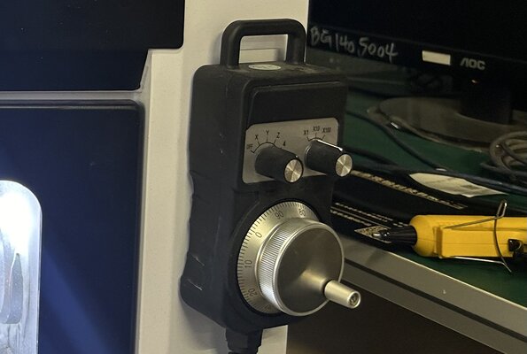
Set the zero points for the tool.
You can move the tool along the X, Y, and Z axes using this controller:
The milling process will start from the bottom-left corner:
-
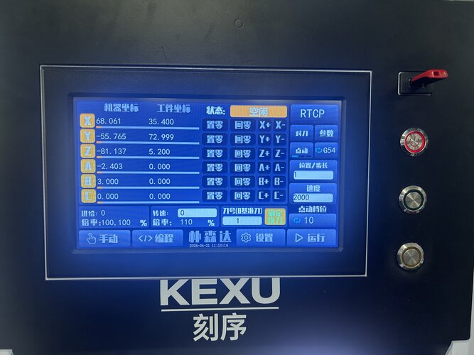
Reset the coordinates to zero.
Since we manually moved the axes, the coordinates are no longer zero.
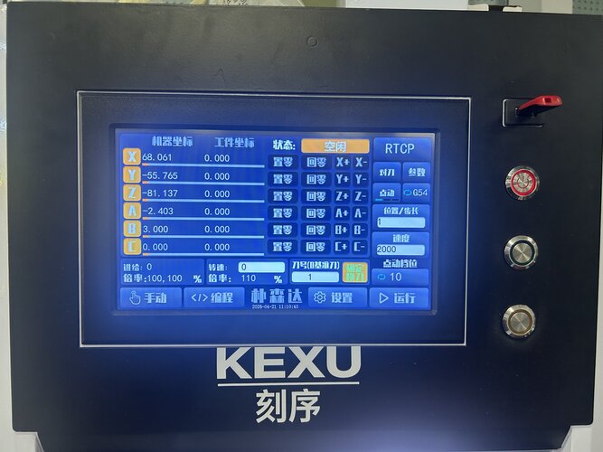
Press “手动” (Manual) to display coordinates:

This window will appear:
Press “置零” (Set Zero):
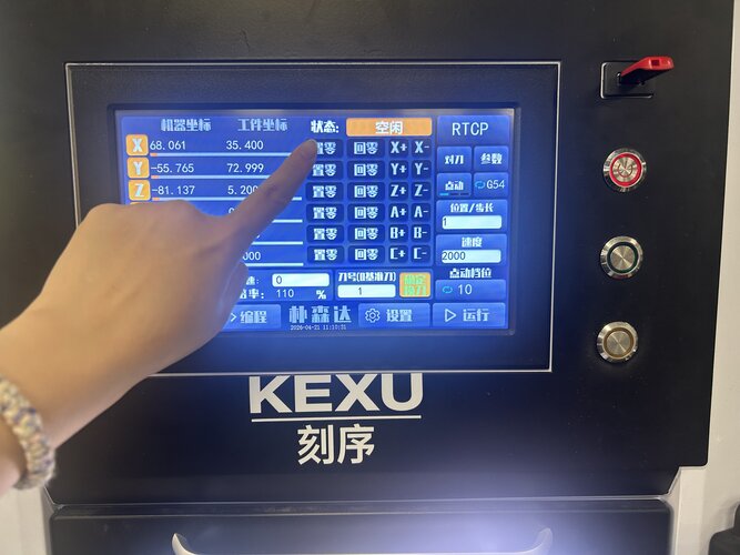
Then confirm:
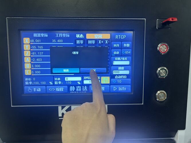
Repeat for X, Y, and Z until all values are zero:
-
Select the file to start milling.
Press “运行” (Run) to select the file:

I milled the traces first, so I chose the traces file first:
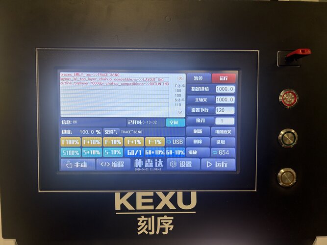
Then press “运行” (Run) red button to start the process:

After I finished milling the traces, I milled the outline:
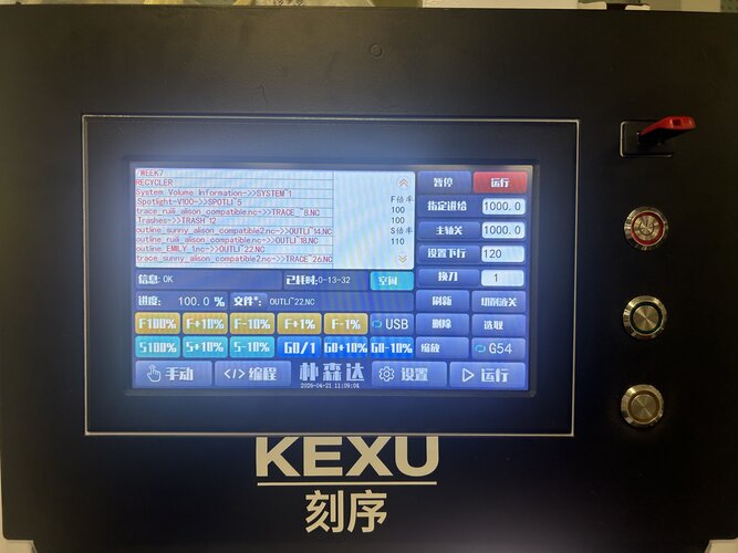
⚠️ The touchscreen is very sensitive, so select your file carefully.
-
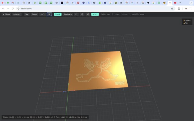
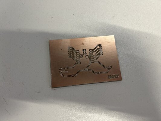
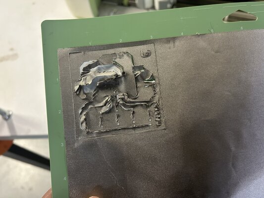
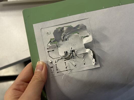
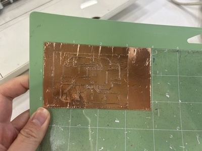
The final result:
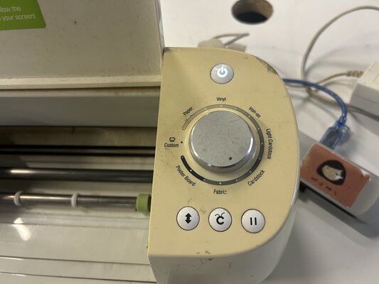
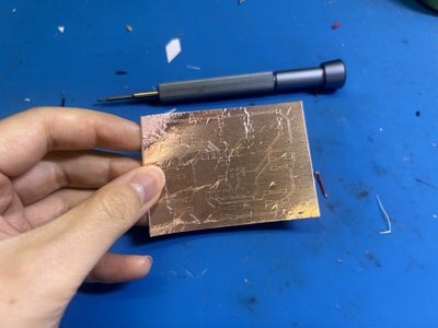
Vinyl Cutting
Failure
(18 Mar 2026) I made several attempts, but they all failed. The blade was already dull, so I asked my instructor to purchase a new 60° blade.
-
I used conductive gray paper as the material:
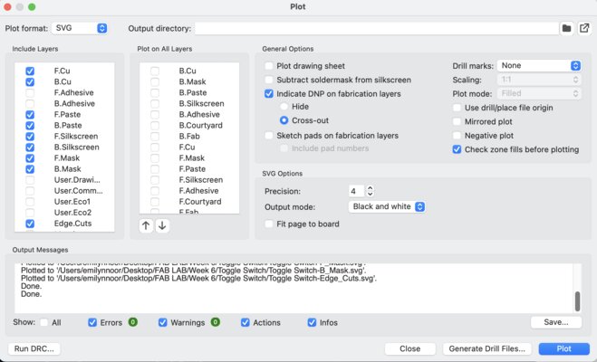
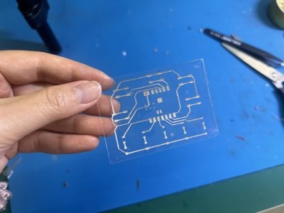
First, I saved my PCB design in KiCad as an SVG file.
Go to:
File → Plot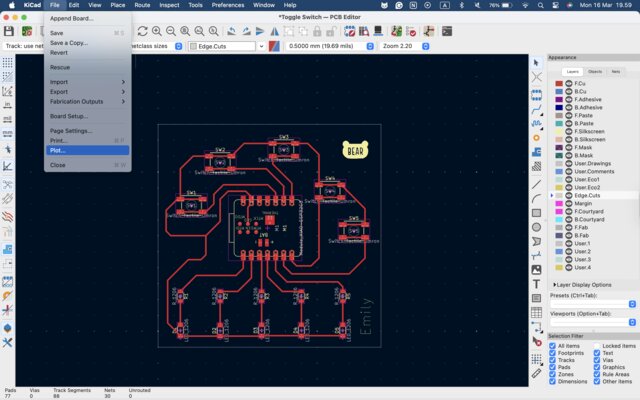
Then, this window will appear:
I opened the SVG file, arranged the design, and converted it to a PNG file:
I also added some text and a logo:
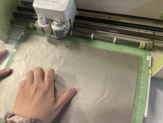
I tried to cut the PCB design using a Cricut Explorer on this material, but all attempts failed. Regardless of whether I used low or high settings, the results were unsuccessful—the paper kept curling up as shown below:
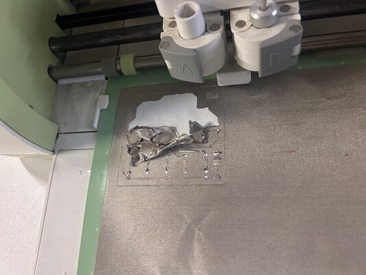
I tried different cut settings:
I also tried mirroring the design and cutting it on the other side of the paper:
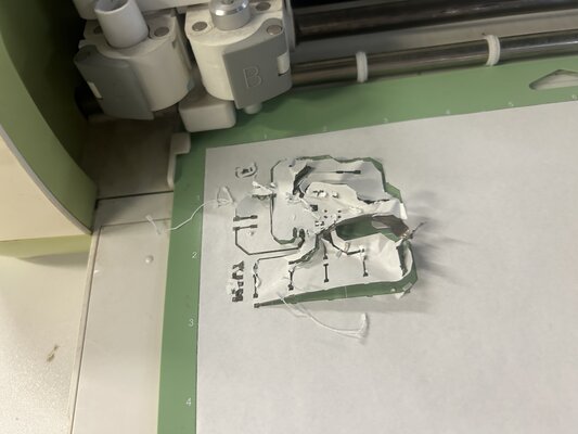
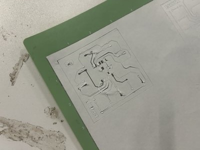
However, all attempts failed.
-
Therefore, I tried using a different material and found copper tape:
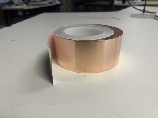
My design dimensions were 7 × 7 cm, but the copper tape width was only 6 cm. Therefore, I needed to adjust my design to fit the tape. Here is the updated design:
I referred to Eduardo Chamorro’s documentation, where he used a PVC sheet as a base and placed copper tape on top. Inspired by this, I tried a similar approach.
I placed the copper tape on top of a PVC sheet and cut it:
However, I was not able to remove the unwanted copper tape from the PVC sheet.
-
I also tried the same method using conductive gray paper on a PVC sheet. This time, I successfully cut it and performed the weeding process:
However, when I tried to solder the gray paper material, it melted…
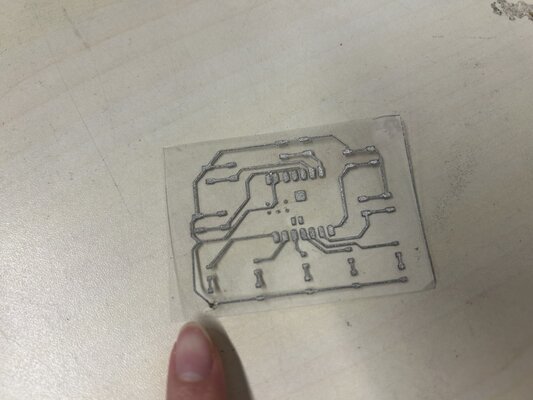
Even though I did not succeed in producing a PCB using the vinyl cutter, I learned a new skill: WEEDING.
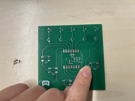
Submit a PCB design to a Board House (JLCPCB)
on 16 March 2026, I submitted my PCB design to JLCPCB. Since I am based in Shenzhen, I wanted to try ordering from the China website, but I was not able to sign up because I do not have a Chinese phone number.
-
Before going to the JLCPCB website, I first prepared the Gerber files (.gbr) in KiCad:
Go to:
File → Fabrication Outputs → Gerbers (.gbr)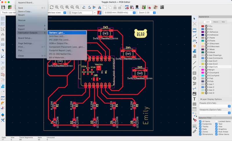
Then, this window will appear:
You can choose which layers you want to export. I selected the following layers: F.Cu, B.Cu, F.Paste, B.Paste, F.Mask, F.Silkscreen, B.Silkscreen, F.Mask, B.Mask, Edge.Cuts
-
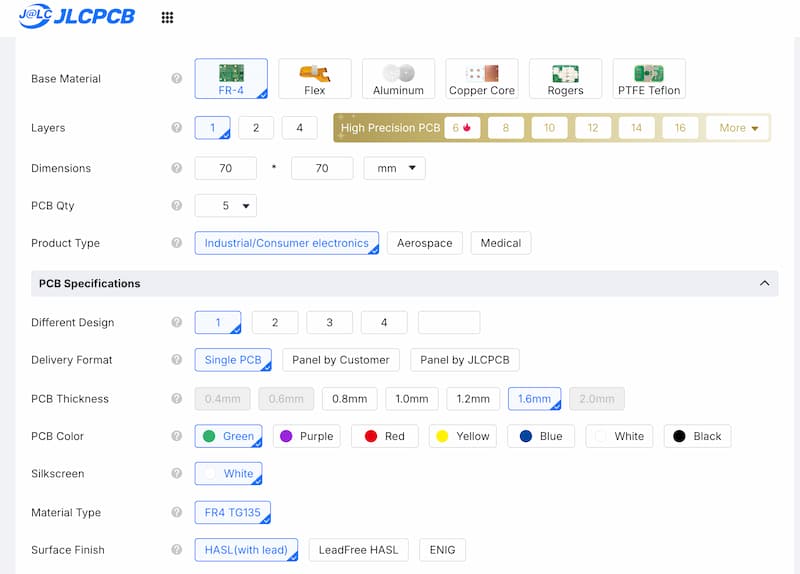
Next, I opened the JLCPCB website and uploaded the Gerber files.

-
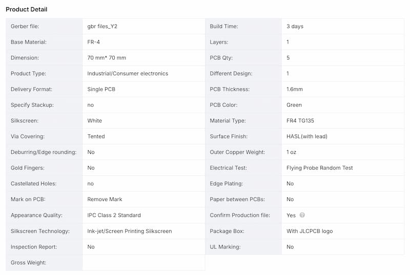
Then, I selected the specifications:
- Base Material: FR-4
- Layers: 1
- Dimensions: 7 x 7 cm (according to your design)
- PCB Qty: 5 (minimum quantity is 5)
- Product Type: Industrial/Consumer electronics
- Different Design: 1
- Delivery Format: Single PCB
- PCB Thickness: 1.6mm
- PCB Color: Green
- Silkscreen: White
- Material Type: FR4 TG135
- Surface Finish: HASL (with lead)
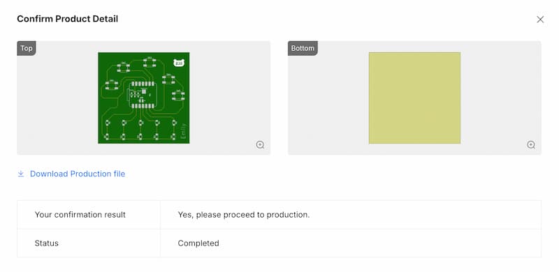
- Confirm Production File: Yes
Once everything was correct, I made the payment. Here is the cost breakdown:
Description Price 5 Circuit Board USD $3.14 (€2.73) Shipping USD $2.04 (€1.77) Discount -USD $2.04 (€1.77) Grand Total USD $3.14 (€2.73) 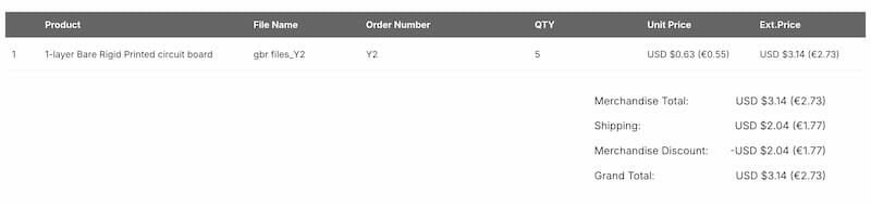
The order has been placed:
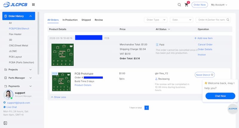
We can check the detailed production progress in the Order History tab:
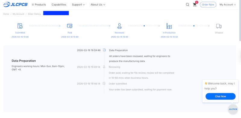
Since I selected Confirm Production File, I received an email the next day to confirm the production files. After confirming, production started.
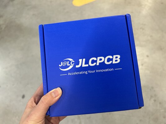
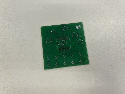
(22 March 2026) My first PCB board from JLCPCB has arrived!
INDIVIDUAL ASSIGNMENT
Make and Test an Embedded Microcontroller System
(18 March 2026) Since I have not yet succeeded in producing the PCB board, I have not completed building and testing an embedded microcontroller system.
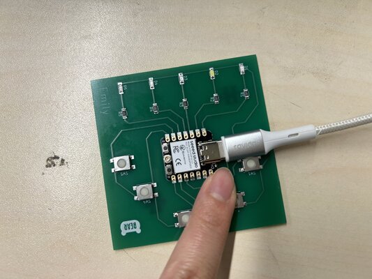
(23 March 2026) My PCB board from JLCPCB just arrived yesterday, so I tried to build and test the embedded system using it.
JLCPCB Board
-
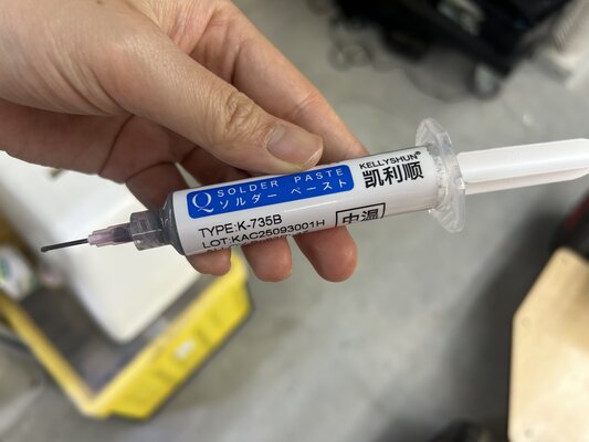
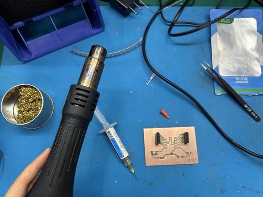
First, I used solder paste to hold the components on the PCB. I applied a small amount of solder paste and placed the components on top. I started with the buttons to practice because they are slightly bigger than the other components (resistors and LEDs).
Info
To preserve its quality and usability, solder paste should be stored in the fridge after use.
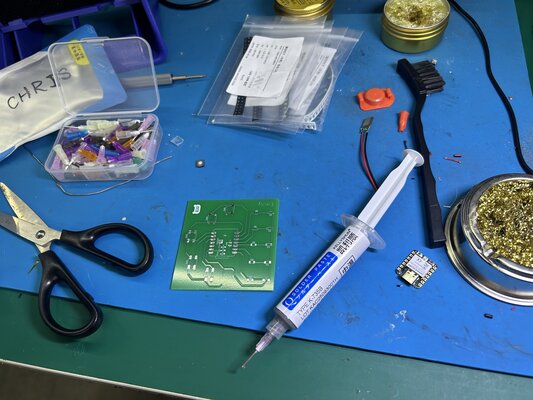
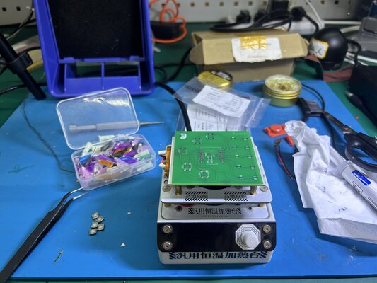
I placed the PCB directly on the soldering hot plate while it was turned off, so I wouldn’t have to move it later (to avoid components falling off after placement). Another benefit is that the height makes it easier to assemble the components.
I finished applying the solder paste and placing the buttons:
-
Next, I turned on the soldering hot plate. It heats up and melts the solder paste, allowing the solder to hold the components in place. You can see the heating process in the video below:
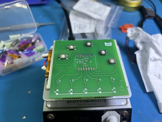
After finishing the buttons, I also assembled the other components (resistors and LEDs).
-
I uploaded the code to the XIAO ESP32C3 microcontroller that I wrote in Week 6 (generated by ChatGPT):
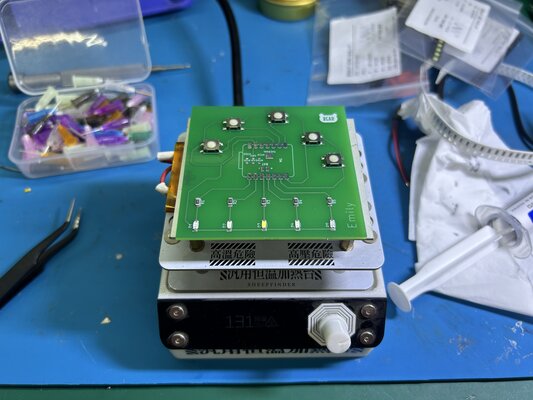
4. Then, I soldered the XIAO ESP32C3 onto the PCB. (I worked on another PCB where I did not place the SW1 button initially, because I had made a mistake: the SW1 button slightly blocked access to the USB-C port.)// LED pins const int led1 = D0; const int led2 = D1; const int led3 = D2; const int led4 = D3; const int led5 = D4; // Button pins const int button1 = D9; const int button2 = D8; const int button3 = D7; const int button4 = D6; const int button5 = D5; // LED states (remember ON or OFF) bool ledState1 = false; bool ledState2 = false; bool ledState3 = false; bool ledState4 = false; bool ledState5 = false; // Previous button states bool lastButton1 = HIGH; bool lastButton2 = HIGH; bool lastButton3 = HIGH; bool lastButton4 = HIGH; bool lastButton5 = HIGH; void setup() { pinMode(led1, OUTPUT); pinMode(led2, OUTPUT); pinMode(led3, OUTPUT); pinMode(led4, OUTPUT); pinMode(led5, OUTPUT); pinMode(button1, INPUT_PULLUP); pinMode(button2, INPUT_PULLUP); pinMode(button3, INPUT_PULLUP); pinMode(button4, INPUT_PULLUP); pinMode(button5, INPUT_PULLUP); } void loop() { // ----- BUTTON 1 ----- bool currentButton1 = digitalRead(button1); if (lastButton1 == HIGH && currentButton1 == LOW) { ledState1 = !ledState1; // TOGGLE digitalWrite(led1, ledState1); delay(200); // debounce } lastButton1 = currentButton1; // ----- BUTTON 2 ----- bool currentButton2 = digitalRead(button2); if (lastButton2 == HIGH && currentButton2 == LOW) { ledState2 = !ledState2; digitalWrite(led2, ledState2); delay(200); } lastButton2 = currentButton2; // ----- BUTTON 3 ----- bool currentButton3 = digitalRead(button3); if (lastButton3 == HIGH && currentButton3 == LOW) { ledState3 = !ledState3; digitalWrite(led3, ledState3); delay(200); } lastButton3 = currentButton3; // ----- BUTTON 4 ----- bool currentButton4 = digitalRead(button4); if (lastButton4 == HIGH && currentButton4 == LOW) { ledState4 = !ledState4; digitalWrite(led4, ledState4); delay(200); } lastButton4 = currentButton4; // ----- BUTTON 5 ----- bool currentButton5 = digitalRead(button5); if (lastButton5 == HIGH && currentButton5 == LOW) { ledState5 = !ledState5; digitalWrite(led5, ledState5); delay(200); } lastButton5 = currentButton5; }After confirming that the code worked properly, I placed the SW1 button on the board. This time, I tried using a hot air gun, but I found that the soldering hot plate is more convenient.
-
After placing the final button, I connected the board to a battery to test how it worked:
It ran smoothly! 🙂
My Mistake
I placed the XIAO ESP32C3 microcontroller in the middle, and the button “SW1” slightly blocks access to the USB-C port. It still works, but next time it would be better to place the microcontroller on the side so it’s easier to plug in the USB-C cable.
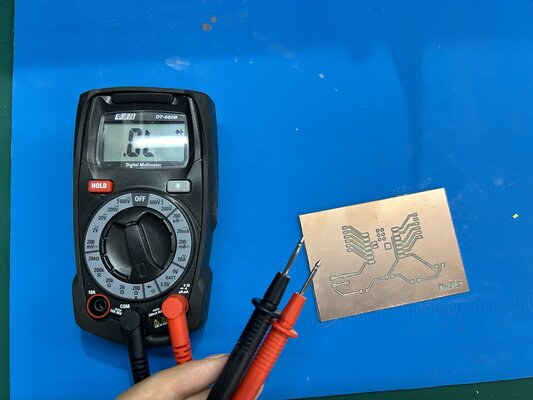
CNC Milling Board
Iteration 1
(Updated on 23 April 2026)
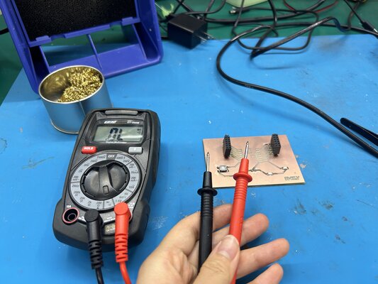
Firstly, I checked the electrical connections using a multimeter to ensure that all the copper traces were functioning properly and were not damaged.
Next, I placed the components onto the board using solder paste and a hot air gun.
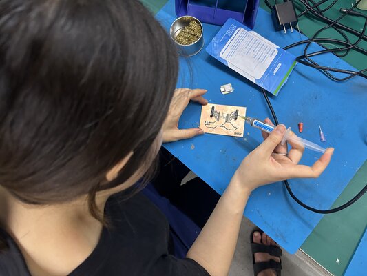
After placing all the components, I checked the connections again to verify that everything was working correctly.
This is the final result after all components were assembled:
Lessons from the First Iteration
The initial circuit failed due to a short circuit. Excessive solder application created unintended bridges between the copper pads and the ground plane. Consequently, I had to restart the process and remill the PCB.
Iteration 2
I repeated the milling process to produce a clean board:
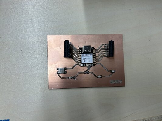
Here is the assembled second iteration:
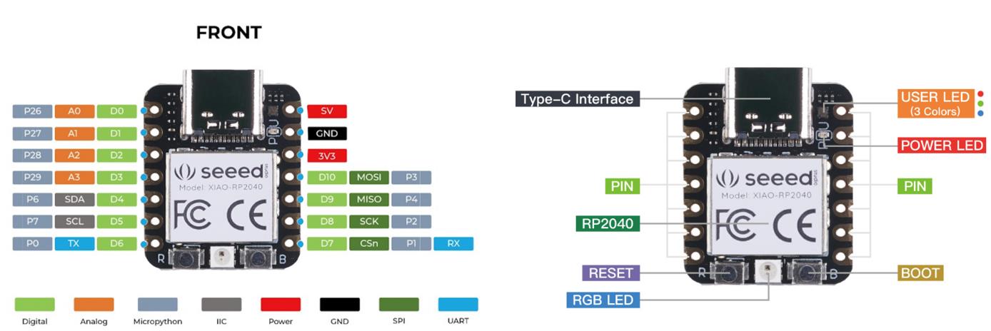
For this version, I opted for male pin headers for the socket and selected the Seeed Studio XIAO RP2040 as the microcontroller.
Trace Fragility
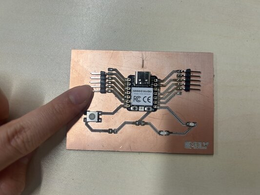
During assembly, the copper trace connected to pin D9 peeled off the substrate. This usually happens when traces are too thin to withstand the heat of the soldering iron or mechanical stress. To improve durability, I will increase the trace width to 1mm in my next design.
In this setup, I connected a 0.96” OLED display (I²C) to the XIAO RP2040. Note that on this specific microcontroller, the default I²C pins used in this project are D4 (SDA) and D5 (SCL).
-
Prepare the materials needed:
- XIAO RP2040
- Jumper Wires (for modular connections)
- OLED display (0.96”, I²C)
OLED display (0.96”, I²C)
The 0.96-inch OLED display is a compact monochrome screen commonly used in embedded systems. It is based on the SSD1306 driver and communicates via the I²C protocol, requiring only two data lines (SDA and SCL).
Key Features:
- Resolution: 128 × 64 pixels
- Interface: I²C (address typically 0x3C)
- Low power consumption (no backlight required)
- High contrast and visibility, even in low-light conditions
- Suitable for text, graphics, and simple animations
-
Circuit Connections:
- Connect the OLED display: SDA -> D4 and SCL -> D5
- Push Button: D6
-
Power Connection:
Connect the XIAO RP2040 to your computer using a USB-C cable.
-
Upload the Code:
After assembling the new board, I uploaded the following code using the Arduino IDE:
(This code was generated using Gemini.)
5. Final Result#include <Wire.h> #include <Adafruit_GFX.h> #include <Adafruit_SSD1306.h> // Screen Dimensions #define SCREEN_WIDTH 128 #define SCREEN_HEIGHT 64 #define OLED_RESET -1 #define SCREEN_ADDRESS 0x3C // Explicit Pin Definitions for XIAO RP2040 #define PIN_SDA D4 #define PIN_SCL D5 #define BUTTON_PIN D6 Adafruit_SSD1306 display(SCREEN_WIDTH, SCREEN_HEIGHT, &Wire, OLED_RESET); int faceIndex = 0; bool lastButtonState = HIGH; void setup() { Serial.begin(115200); pinMode(BUTTON_PIN, INPUT_PULLUP); // 1. Explicitly configure I2C Pins for RP2040 before calling Wire.begin() Wire.setSDA(PIN_SDA); Wire.setSCL(PIN_SCL); Wire.begin(); // 2. Initialize OLED if(!display.begin(SSD1306_SWITCHCAPVCC, SCREEN_ADDRESS)) { Serial.println(F("SSD1306 allocation failed. Check wiring on D4/D5!")); for(;;); } // 3. Initial Display Setup display.clearDisplay(); display.setTextColor(SSD1306_WHITE); // Set default color to White drawFace(faceIndex); } void loop() { bool currentButton = digitalRead(BUTTON_PIN); // Button Press Detection (Active Low) if (lastButtonState == HIGH && currentButton == LOW) { faceIndex = (faceIndex + 1) % 5; // Cycle 0 to 4 drawFace(faceIndex); delay(200); // Debounce delay } lastButtonState = currentButton; } void drawFace(int face) { display.clearDisplay(); // Draw expressions in SSD1306_WHITE switch(face) { case 0: // 😊 Happy display.fillCircle(40, 25, 6, SSD1306_WHITE); display.fillCircle(88, 25, 6, SSD1306_WHITE); display.drawCircle(64, 35, 20, SSD1306_WHITE); // Smile break; case 1: // 😢 Sad display.fillCircle(40, 25, 6, SSD1306_WHITE); display.fillCircle(88, 25, 6, SSD1306_WHITE); display.drawCircle(64, 65, 20, SSD1306_WHITE); // Frown break; case 2: // 😠 Angry display.fillCircle(40, 30, 6, SSD1306_WHITE); display.fillCircle(88, 30, 6, SSD1306_WHITE); display.drawLine(30, 15, 50, 25, SSD1306_WHITE); // Left brow display.drawLine(78, 25, 98, 15, SSD1306_WHITE); // Right brow display.drawFastHLine(44, 55, 40, SSD1306_WHITE); // Flat mouth break; case 3: // 😞 Disappointed display.drawCircle(40, 25, 6, SSD1306_WHITE); display.drawCircle(88, 25, 6, SSD1306_WHITE); display.drawFastHLine(44, 50, 40, SSD1306_WHITE); break; case 4: // 😍 Love // Heart Eyes display.fillTriangle(30, 25, 40, 10, 50, 25, SSD1306_WHITE); display.fillTriangle(78, 25, 88, 10, 98, 25, SSD1306_WHITE); display.drawCircle(64, 35, 20, SSD1306_WHITE); break; } display.display(); }The system successfully cycles through five different expressions with each button press. Here is the final demonstration:
Iteration 3
Info
In this iteration, I aimed for a more compact and simplified PCB design. I used 1mm-wide traces to ensure better reliability and easier milling.
I utilized this PCB for both the Week 9 (Input Devices) and Week 10 (Output Devices) assignments.
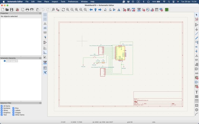
Schematic Design:
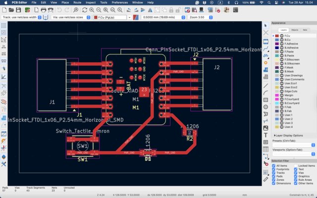
PCB Design:
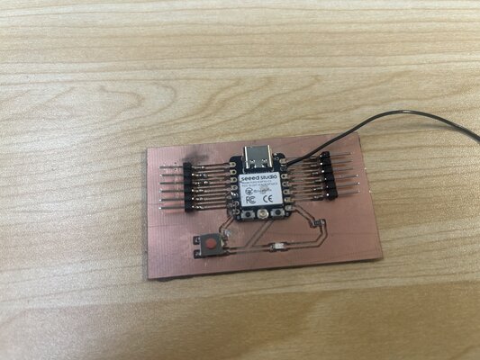
The assembled board:
Files
KiCad Files