8. Electronics design
Group assignment:
- Use the test equipment in your lab to observe the operation of a microcontroller circuit board (as a minimum, you should demonstrate the use of a multimeter and oscilloscope)
- Document your work on the group work page and reflect what you learned on your individual page
Unfortunately, due to my knee operation i was unable to attend at Waag for the group assignment, but i hope to document the use of the oscilloscope in the upcoming weeks and document the results here.
Individual assignment:
- Use an EDA tool to design a development board to interact and communicate with an embedded microcontroller
KiCad
This week we were introduced to Kicad, an open sourced design software for creating pcb's.
I asked Brew to install KiCad for me, which worked great, but I was left with multiple apps on my mac and it wasn't the most up to date version. This also became an issue, because I was'nt navigating through the software in the right way. I opened the schematic editor first and starting the process from there and not actually creating a project.
Steps I should have taken:
- Download the latest version of KiCad
- Download and install the Fab library
- Create a new project
- Set the design rules
- Design your pcb, keeping in mind component placement and traces
- Export files for milling
What I did
I started this week by working backwards to find all the components I needed for my final project and then design a board around that. This was going "ok", but then I was having some trouble locating some parts in the library and also discovered that I didn't have the fab library installed.
so...
Installing Fab Library
First you need to click here to get to the repository, there you can follow the steps to download the fab library.
- Clone or download this repository. You may rename the directory to fab.
- Store it in a safe place such as ~/kicad/libraries or C:/kicad/libraries.
- Run KiCad or open a KiCad .pro file.
- Go to "Preferences / Manage Symbol Libraries" and add fab.kicad_sym as symbol library.
- Go to "Preferences / Manage Footprint Libraries" and add fab.pretty as footprint library.
KiCad not compatible with library
Even with the library installed I ran into some issues. I was using KiCad 7, but that seemed outdated and I would get an error message on the schematics.
To resolve that, I downloaded the latest version of KiCad from there homepage here .
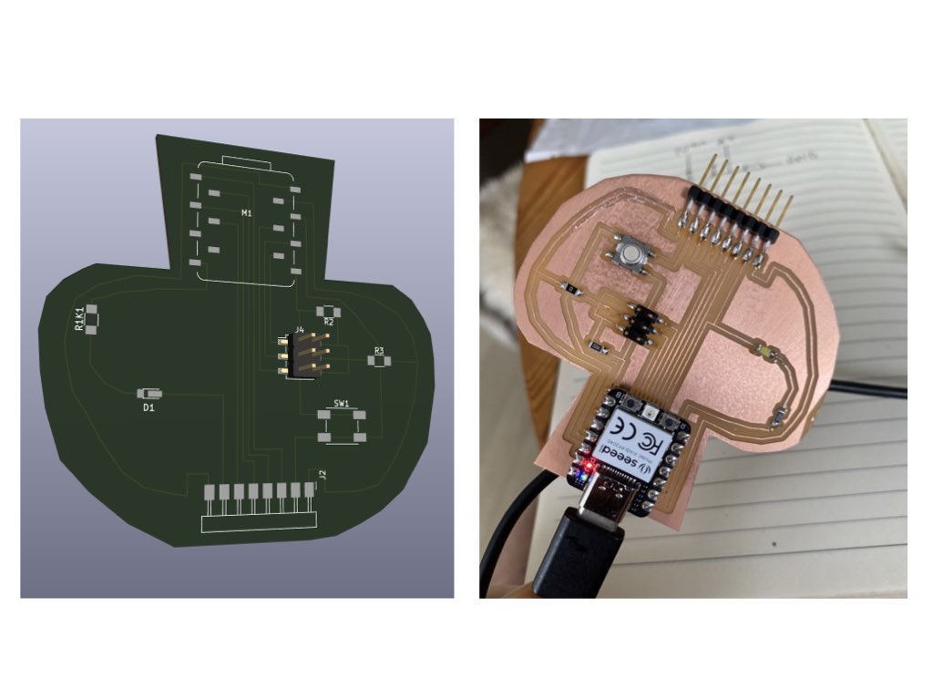
So, with the fab library installed and a new project opened I could go about designing my board. My original idea was to copy Adrian Torres, but add more I/O's. That soon became too taxing and left me with lots of trace lines and a board I wasn't quite happy with. Part of me had lost that fun guy I always aspired to be, so I went back to the drawing board.

I then simplified the design by removing some I/O's and change the positions of the components so that I could have a better chance of connecting everything together. Then the fun guy was back in action.

Design rules
At this point it's good to state how important design rules are and at what point they should be implemented, at the start of course.
To edit design rules:
File -> Board setup
Then we want to set up:
- constraints
- pre defined sizes: Typically 0.4 for what we need
- Net classes
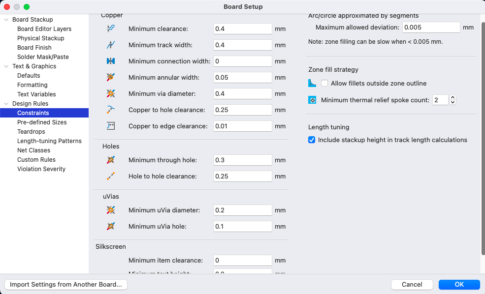
I had my design made before I defined the design rules, so this meant that when I came to mill, the G-code file said that my lines where 0.2mm. This meant there were no traces left when the milling bit tried to leave such a small trace.
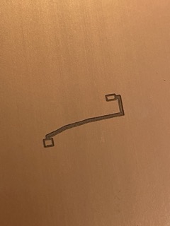
When I went back to the design I had to edit each individual line segment by using the E shortcut to bring up the segment properties and changing line thickness.

Exporting svg files
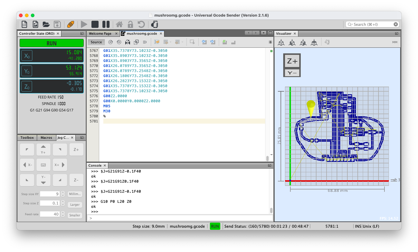
To mill the design we need to export 2 svg files. One for the trace lines and one for the edge cut. Simple go to: file: export... and the we select the parameters as shown below.

The files will be saved on your KiCad project folder as svg files with your project name and an ending of -F_Cu & -Edge_Cuts. We select the files in mods. For the trace lines we have to invert the image, this creates a negative with only the trace lines. Once we have our parameters set up and we are happy we can calculate to generate the G-code that can be sent to the milling machine.
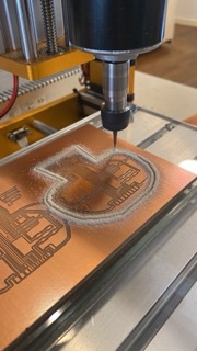
Milling the PCB
I had some "fun" milling the mushroom, it's waaaay bigger than was expecting, next time I'll make it neater. It wasn't smooth sailing, let me tell you. As mentioned, the traces were being removed due to the width being set to 0.2mm. Once that was resolved I set out to start milling again.
I prefer the 0.4 end mill, I think with the right setting it produces the cleaner finish, unfortunately they're incredibly brittle, I think it has a good 10 minutes of action before the inevitable happened.

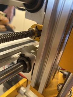
After that I was given a 0.25mm tapered bit and made a test cut before staring, everything seemed ok so then i started milling. With the mushroom almost complete, the machine started milling outside of the design lines. Henk was sure I paused the machine mid process, but then we found a loose nut on the xy spindle bar that had caused it to loose its position.
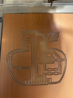
I was able to persist with the milling and have a managed to make the mushroom pcb. It's not pretty and some of the copper wasn't milled properly, so i have had to use a knife to carefully remove what was left behind and complete the traces.
Programming
Using the arduino IDE I was able to programme the board and test the LED. The rapid blink I used in week 4 worked just fine, but when i tried anything relating to the button I was shorting the circuit.
Debugging
So there is a short circuit when I press the button suggesting that my 3V is connecting to ground.
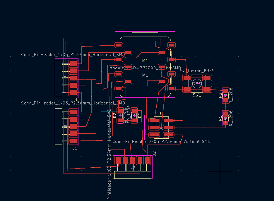
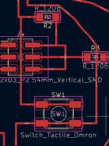
I think I have found a possible issue, in the hast of making the pcb in KiCad, I just thought that blue lines were always indicating where your traces go, instead of actually thinking how the components work. In doing that, I have connected the button across pins and I'm also passing my PWR 3V to another component via the switch.
I will have to edit the drawing and prepare another mushroom for milling.
Design Files
Learning outcomes
- Select and use software for circuit board design [x]
- Demonstrate workflows used in circuit board design [x]
Have you answered these questions?
- Linked to the group assignment page
- Documented what you have learned in electronics design
- Checked your board can be fabricated
- Explained problems and how you fixed them.
- Included original design files (Eagle, KiCad, etc.)
- Included a ‘hero shot’