
8. Electronics Desing
Overview
This week's group assignment was to use the lab test equipment to observe the operation of a microcontroller printed circuit board.
Through observing the tests performed in the lab with multimeters and oscilloscopes by my group, I have learned
fundamental aspects about electronic design and gained a deeper understanding of circuit behavior under various
conditions. By seeing how characteristics such as continuity, resistance, voltage were measured and how electronic signal
waveforms were analyzed, I gained a better understanding of the functionality of PCB designs and the dynamic behavior of
components under electrical load.
You can consult the group assignment at the following link.
KiCad
KiCad is an open source software for the design of printed circuit boards (PCBs) and electronic schematics. It allows users to create complex circuit board designs with tools to draw schematics, design the PCB layout, and visualize in 3D the final assembly of the components on the board. KiCad supports a wide range of electronic components and offers features such as design rule checking (DRC) and file generation for circuit fabrication.
This week's assignment was to use an EDA tool to design a development board to interface and communicate with an embedded microcontroller.
The first thing I did was to install the software by following the steps below:
- Visit the official KiCad website at the following link.
- Click on the "download" button and choose your operating system, in my case Windows.
- After downloading the version of your choice, open the file to start the installation process.
- Follow the installation instructions (accept the terms, choose the destination folder, etc.).
- Finally, open the software.
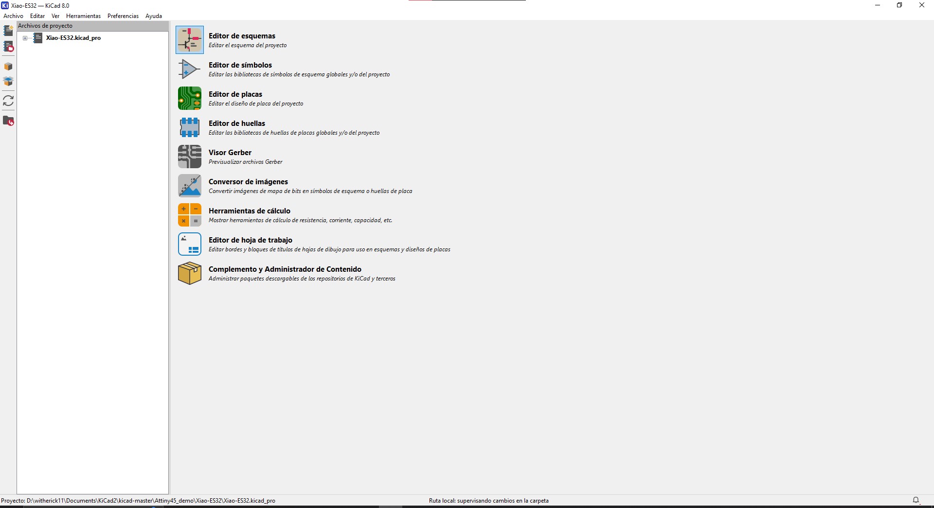
When you open the software, a window will be displayed with many options and tools to use. The most prominent ones are Schematic Editor and Board Editor.
Before making the PCB design, we will first install a library, this library is to access the components that the university has. This library was given to us by the professors of fablab. The reason is to work with components that the university has and avoid buying components that are not available.
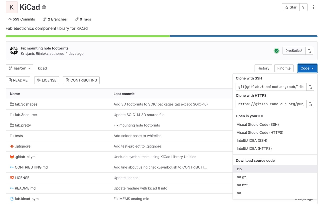
First we have to download the library to our computer. The fablab teachers shared it with us. It was in a repository in Gitlab. What I did was to download it in .zip as shown in the image.
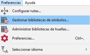
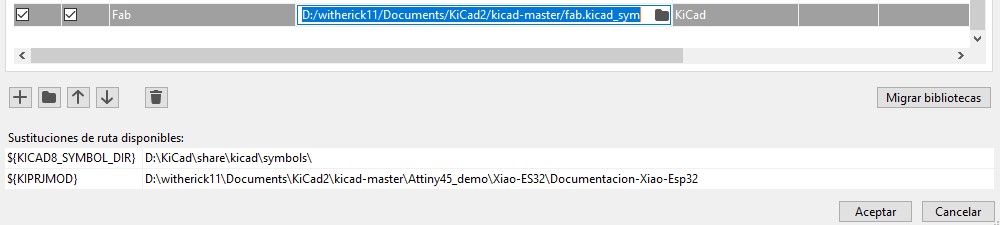
In KiCad select the Preferences option and click on Manage symbol libraries. A small window with all the libraries that KiCad has installed by default will be displayed.
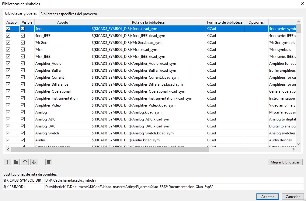
The next step is to add a row with the "+" button. We assign a name to it, in my case I named it Fab, with this name we will be able to look for the components in an easier way. The folder that we downloaded from Gitlab we unzip it and save it in our computer. This is because next to Fab, we will select the file fab.kicad_sym that is in the folder we downloaded.
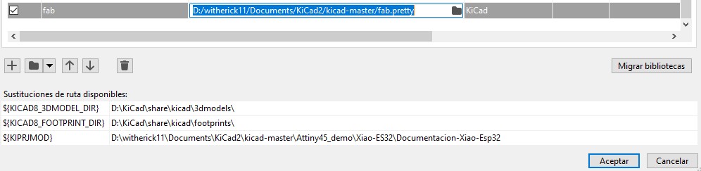
Accept and select the Preferences option again. Now we select the option Manage footprint libraries. A window similar to the previous one will appear.
We will do the same steps as we did before. We add a row with the "+" button. We write fab in lowercase and to the right we now add the file fab.pretty.
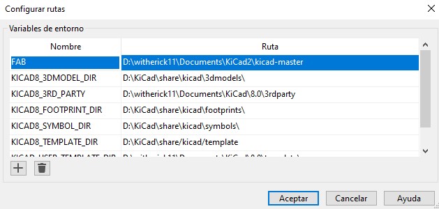
Finally, we select the Configure routes option in Preferences. When the window pops up, type FAB in capital letters and select the entire folder you downloaded.
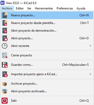
To start with the design, we must first create a new project. To do this, select the File option and select New Project. Then we choose the path to save the project on our computer and name it.
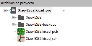
After creating a new project the following files will appear in KiCad.
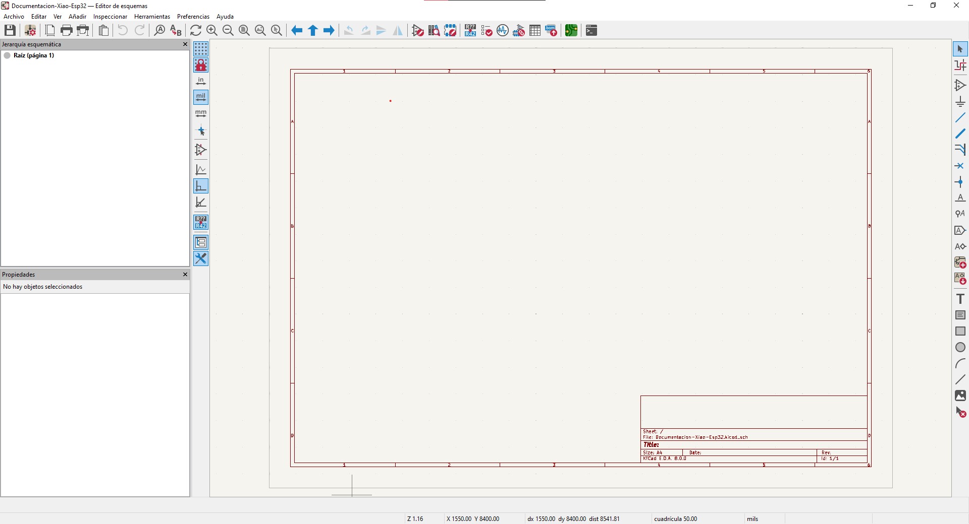
Next, we will do the schematic design. To do this layout, we select the file ending in kicad_sch.
When you select this option, another window like the one shown in the following image will be displayed:
Components
In this window we have many tools, the ones I will use are vertically on the right. The first step is to select the components. The tool that I used is Add symbols and it can be used in two ways, the first one is using the tool that is in the image below:
The second way is by using the "a" key on the keyboard.
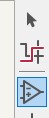
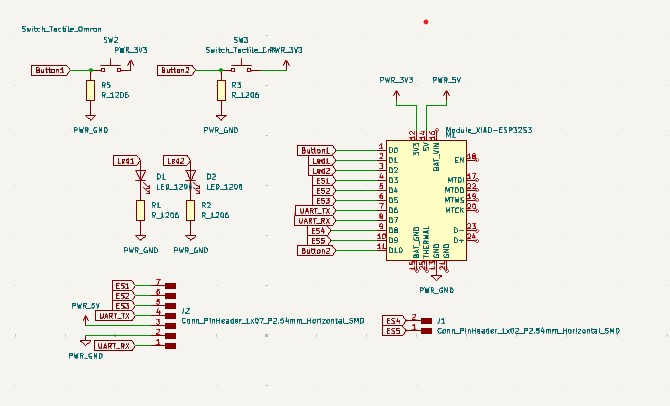
The first component I selected is the microcontroller, the one I used for this week is a Xiao-Esp32C3.
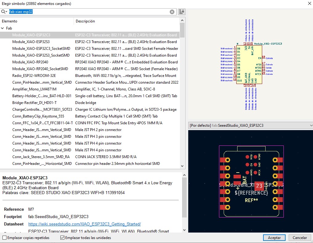
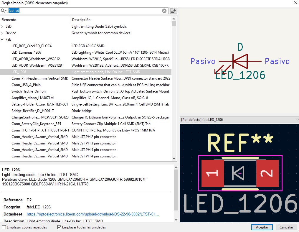
The next components I chose were leds and resistors, I chose the 1206 leds and 1206 resistors.
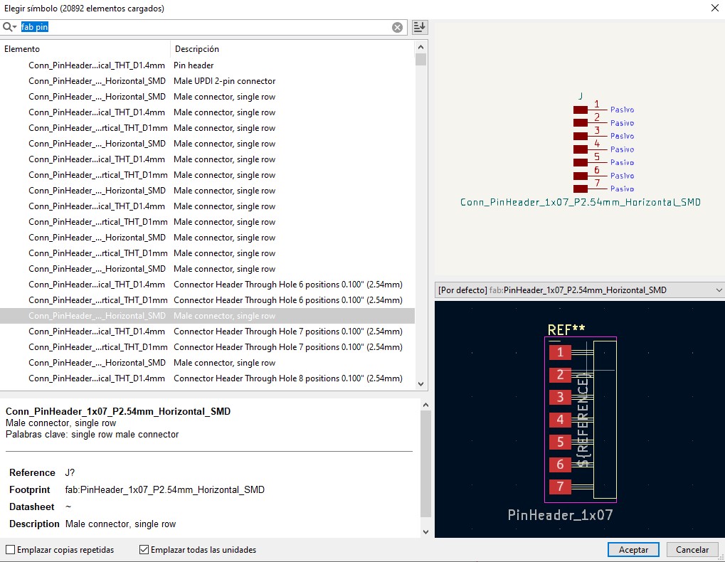
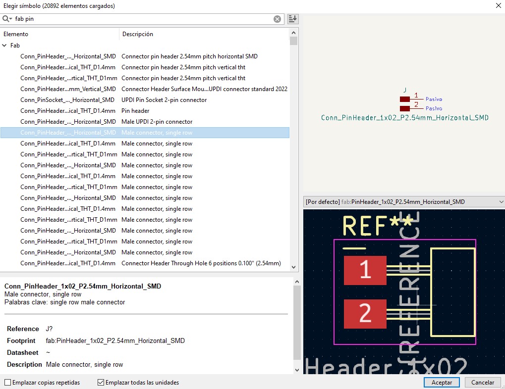
Finally, I chose pins of various sizes. Of 7 and 2.
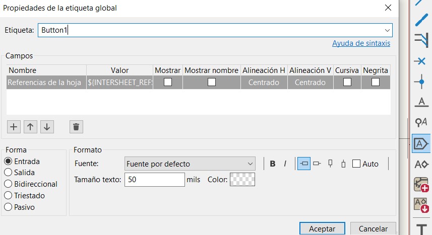
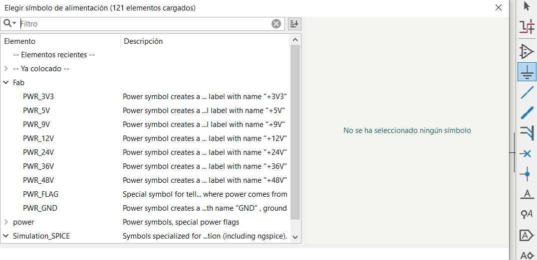
After adding all the components, I arranged them in the window and started labeling them. For the labels I used the Add Global Labels tool. To add PWR and GND I used the Add Power Symbols tool.
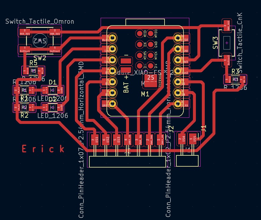
My schematic design looks like this:
After finishing with the schematic design we now move on to the PCB editor.
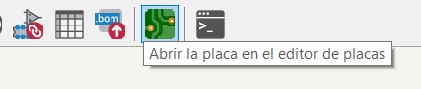
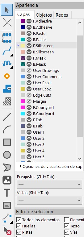
When we select the option, we will see a new window with many tools, the ones we will use are the ones on the right.
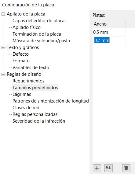
Before starting to join the components we use the Board Configuration tool, set the Minimum Margin to 0.4 mm and the Minimum Track Width to 0.5 mm in Requirements.
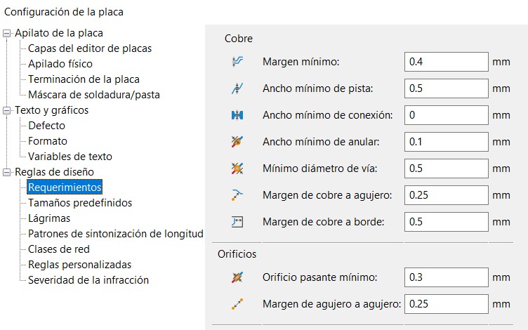
Then we adjust the size of the track in Predefined Sizes, ideally using a size above 0.6 mm. I used 0.7 mm.
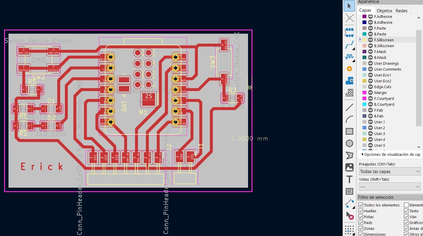
After making the above configurations, what remains to be done is to arrange the components and then join them together. This part can be a bit tedious, as sometimes the wires can cross and some changes have to be made to the schematic design. This is my result:
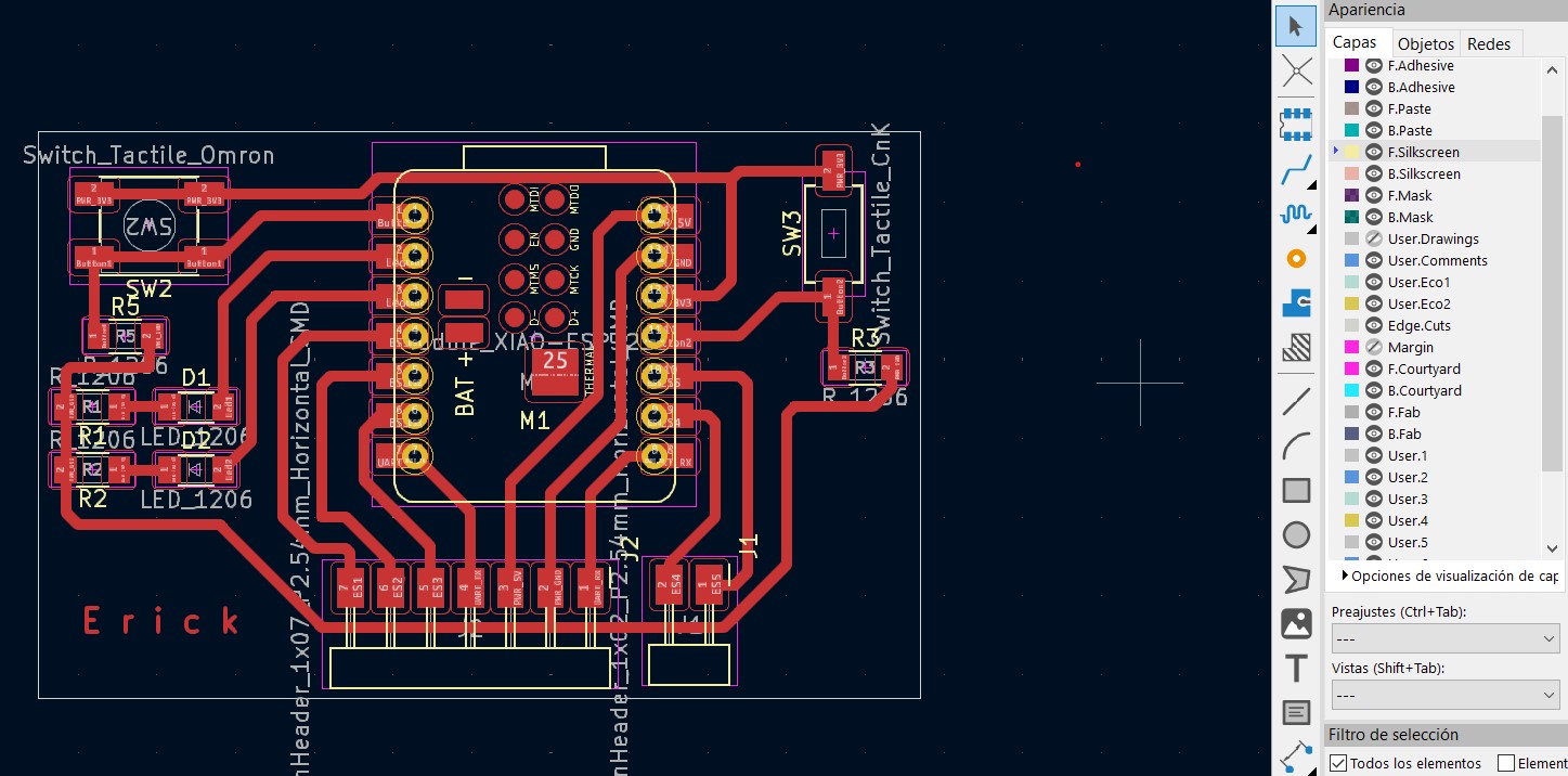
The next step is to create a margin to our circuit, depending on how you want the design of your PCB you will use different tools such as rectangle, circle or polygon. In my case I used the rectangle option. This margin goes in the Edge.cuts layer.
The next step is to create a margin of that rectangle that we made with another one. The new rectangle is saved in the Margin.The margin between both rectangles is 1 mm.
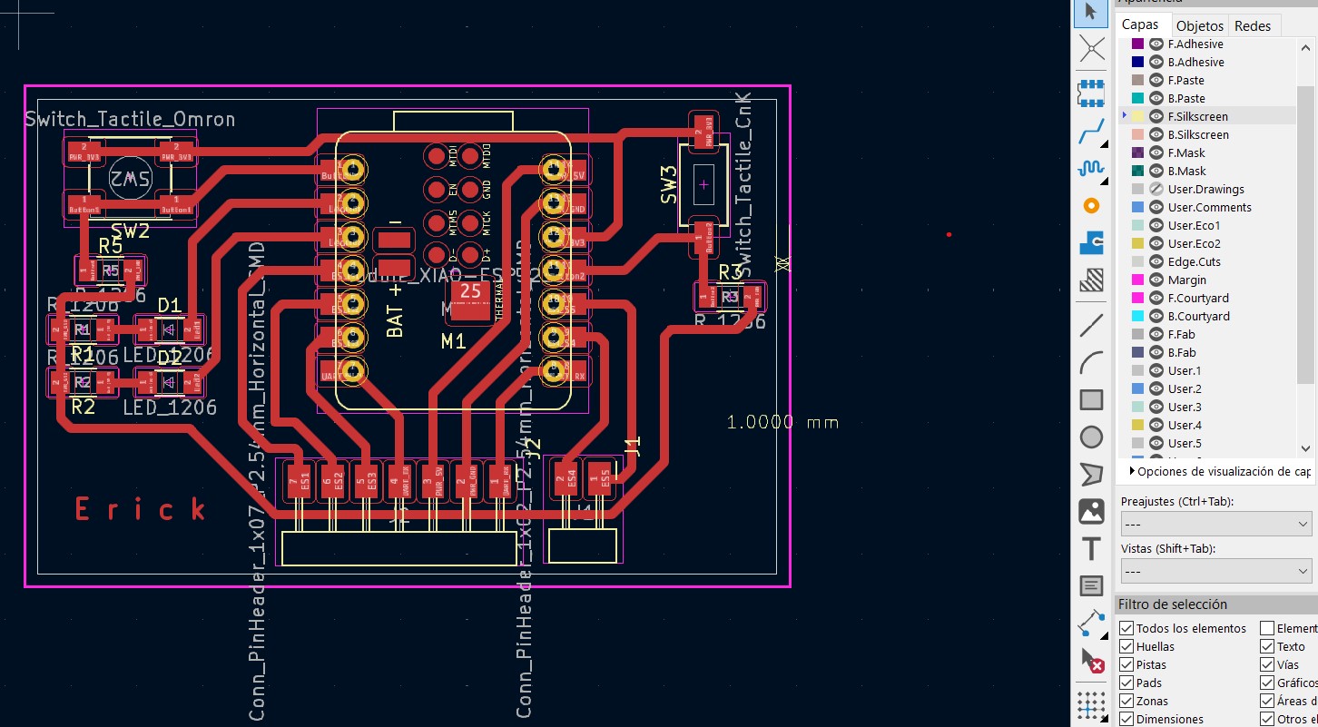
The next step is to use the polygon tool to cover the rectangle inside. We save this figure in the User.drawings layer.
Export files
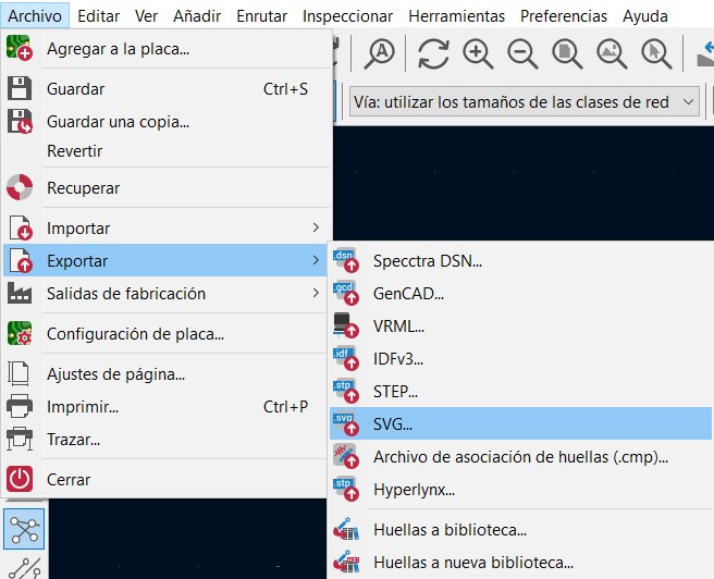
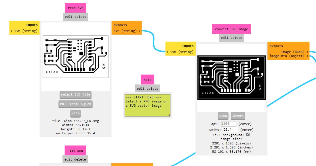
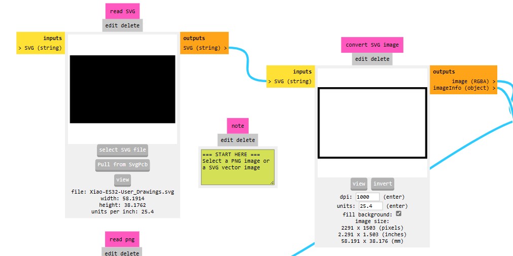
To export the files open File -> Export and choose SVG.
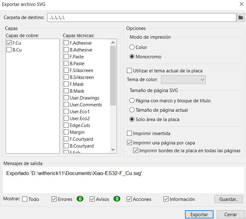
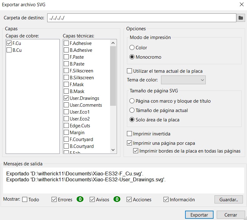
First we export the file that will make the engraving of the board, for this we select F.Cu in Copper Layers and in Technical Layers we do not select anything. In Print Mode we select the option Monochrome and in SVG Page Size, we select Only area of the board. For the other file, the one that will cut the board, we select F.Cu and also User.drawings in Technical layers and use the same settings as above.
Mods
Mods is a modular digital manufacturing tool available at modsproject.org, especially useful for PCB creation, that allows users to design and control manufacturing processes through interconnectable modules. Each module specializes in a different function, from path calculation to CNC machine operation, making it easy to customize workflows and improve efficiency and accuracy in prototype and electronic component manufacturing.
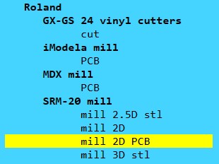
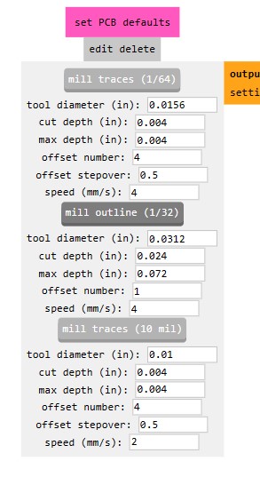
The next step is to use the Mods platform to prepare the files for use on the CNC. The first thing to do is to select the CNC model that the university has, which is the ROLAND SRM-20, where we select the mill 2D PCB option.
The next step is to select the first file that will do the engraving, as we export it in KiCad as SVG, we choose the option Select SVG file. Then, we invert the image, as shown on the right in the image.
For the engraving, we choose the first option mill traces (1/64).
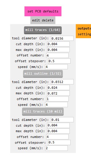
In this window we change the offset number from 4 to 2.
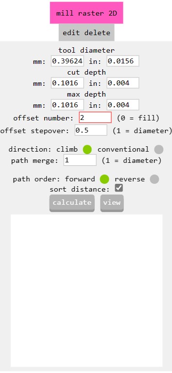
Then, we change x, y and z to 0 and turn on the buttons on the right.
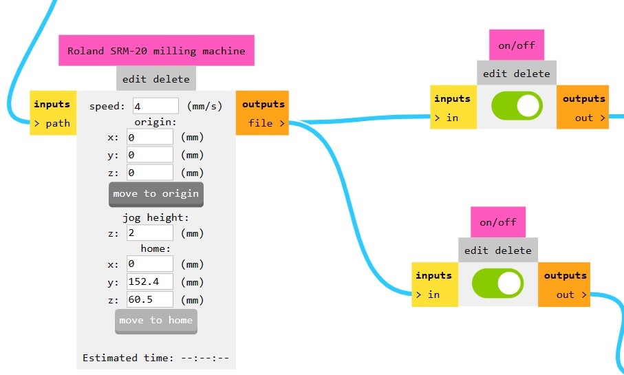
Finally, click on calculate.
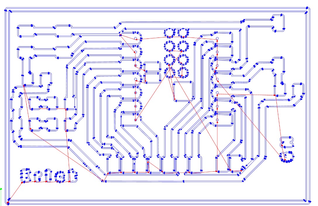
It will give us an .rml file and we will be able to visualize it in view.
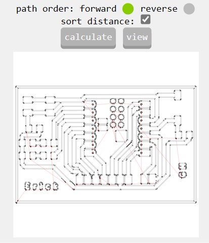
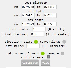
For the cut file, which will cut the plate, we will use the same configuration, we will only change a few things. First we load the cut file and as in the previous file, we invert the image.
What we will modify for this file is the mill outline tool (1/32).
When we change the option, this window will be modified and we will leave it with this configuration. The only thing left to do is to click on calculate. The rest, we leave it with the same configuration, as we have in the trace file.
And this is the result:

Making PCB

For this assignment I used the ROLAND SRM-20 CNC with the following features:
- Cutable Material: Modeling Wax, Chemical Wood, Foam, Acrylic, Polyacetal, Acrylonitrile Butadiene Styrene (ABS), Printed Circuit Boards
- Operational Travels in X, Y, and Z: 203.2 mm (X) × 152.4 mm (Y) × 60.5 mm (Z)
- Loadable Workpiece Weight: 2 kg
- Operation Speed: From 6 mm/min to 1,800 mm/min
- Software Resolution: 0.01 mm/step (RML-1), 0.001 mm/step (NC Code)
- Mechanical Resolution: 0.000998594 mm/step
- Spindle Rotation Speed: Adjustable from 3,000 RPM to 7,000 RPM
- Interface: USB
- Operational Noise: During operation: 65 dB(A)
- External Dimensions: 451 mm (width) × 426.6 mm (depth) × 426.2 mm (height) (17.76 in [width] × 16.80 in [depth] × 16.78 in [height])
- Weight: 19.6 kg
These were the tools I used to be able to work with this machine. To adjust the bits and the copper plate.
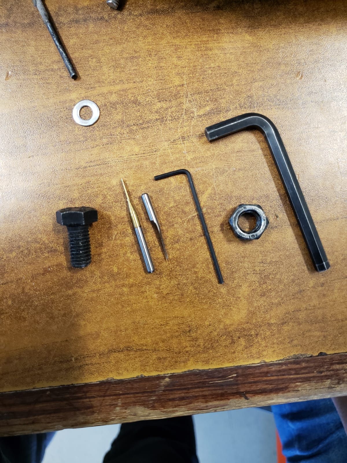
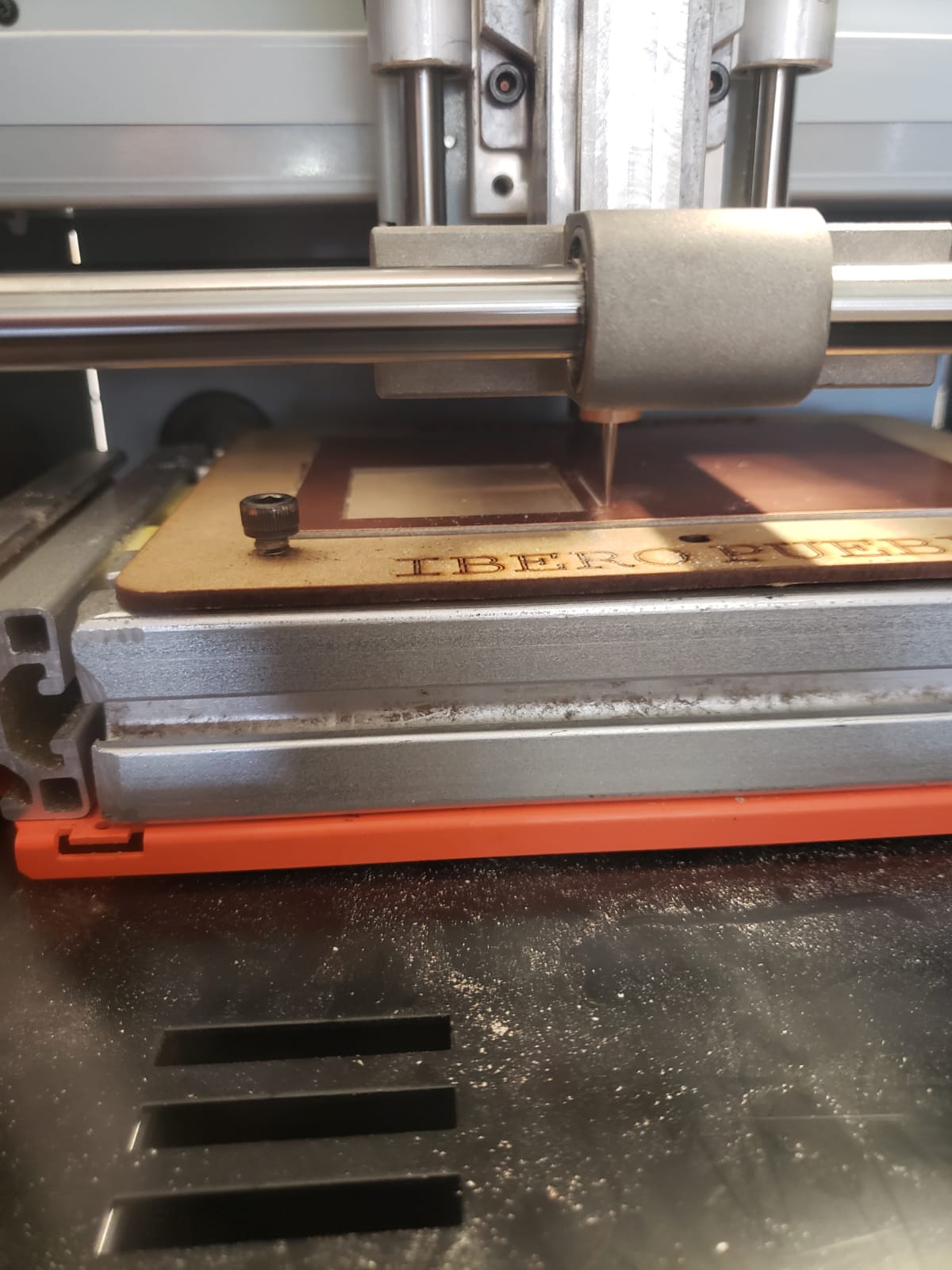
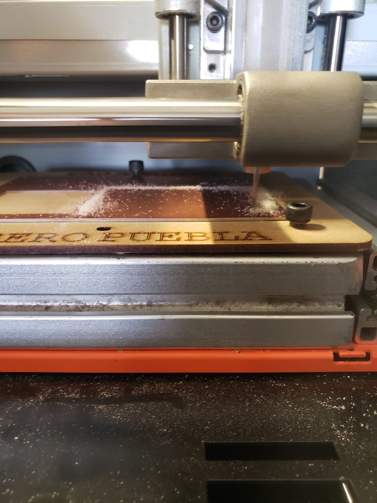
This is a picture of the machine before putting it to work. In order to adjust the position of the tool, I used a lamp to better visualize the position.
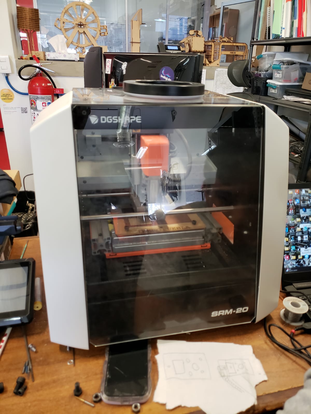
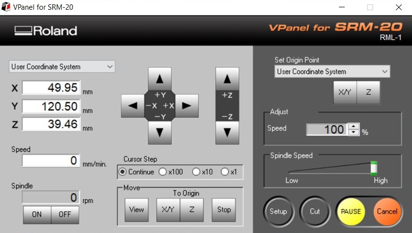
To move the machine we use the machine software called Vpanel for SRM-20. The first thing we adjust is the z-axis, for this we can modify the speed to go slower. When we finish adjusting the tool in the z-axis, we save the position. If we are not sure that the tool is touching the copper plate, we can turn on the spindle and with the spindle on we can adjust the z-axis. Then we adjust the x and y axes, and it's the same step, adjust the tool where we want it and save the position. After setting up the machine, we load our files to start engraving, we do this with the Cut option. First we select the file that will make the stroke and then the file that will make the cut.
The next thing is to wait for the machine to finish engraving and cutting. The day I did this, I didn't take pictures of the final result, because it was late at night and I wanted to go home :(.
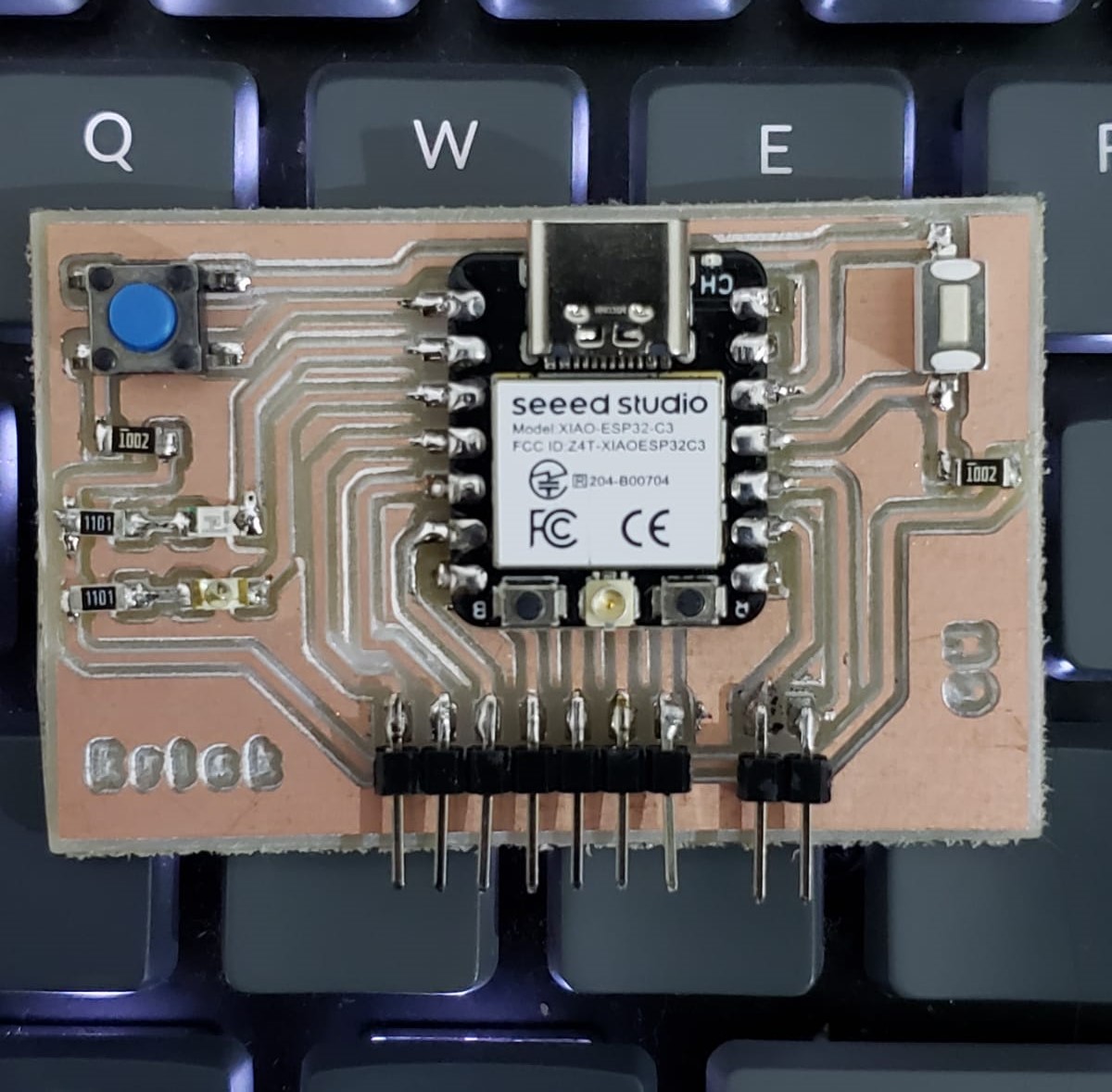
Soldering components
Components
- Microcontroller: Xiao-Esp32C3
- Micro leds: two leds
- R820E-1206 SMD Surface Resistor: two resistors
- Resistor SMD RR0816P-242-B-T5: two resistor
- Buttons: two button
- Pins: nine pins
Unlike the first time I welded, which was in week 4. I noticed that I had less trouble with this part. It was easier to solder my components.
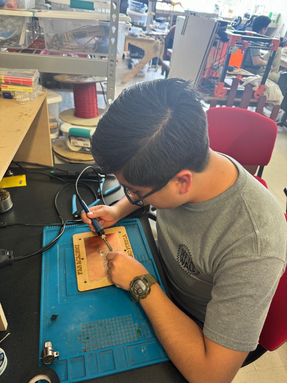
This is the result:
Testing PCB
To test the PCB I visited their website. You can check it at the following link. I followed all the steps on the page to be able to program the board in Arduino IDE.
The following code turns on the LEDs in sequence when I press one button and when I press the other button it turns on both LEDs.
// Define pins for buttons and LEDs
const int buttonPinSeq = D0;  // Pin for the sequence button
const int buttonPinBlink = D10; // Pin for the blink button
const int ledPin1 = D1;   // Pin for the first LED
const int ledPin2 = D2;   // Pin for the second LED

int buttonStateSeq = LOW;  // Current state for the sequence button
int buttonStateBlink = LOW;  // Current state for the blink button
int lastButtonStateSeq = LOW; // Previous state for the sequence button
int lastButtonStateBlink = LOW; // Previous state for the blink button
unsigned long previousMillis = 0; // will store last time LED was updated
const long interval = 250; // interval at which to blink (milliseconds)

void setup() {
    pinMode(buttonPinSeq, INPUT); // Set the sequence button as an input
    pinMode(buttonPinBlink, INPUT); // Set the blink button as an input
    pinMode(ledPin1, OUTPUT); // Set the first LED as an output
    pinMode(ledPin2, OUTPUT); // Set the second LED as an output
}

void loop() {
    int currentButtonStateSeq = digitalRead(buttonPinSeq); // Read the state of the sequence button
    int currentButtonStateBlink = digitalRead(buttonPinBlink); // Read the state of the blink button

    // Check if sequence button state has changed from off to on
    if (currentButtonStateSeq != lastButtonStateSeq) {
    if (currentButtonStateSeq == HIGH) {
        // Run LED sequence only once per button press
        digitalWrite(ledPin1, HIGH); // Turn on first LED
        delay(500); // Wait 500ms
        digitalWrite(ledPin1, LOW);  // Turn off first LED
        digitalWrite(ledPin2, HIGH); // Turn on second LED
        delay(500); // Wait 500ms
        digitalWrite(ledPin2, LOW);  // Turn off second LED
    }
    lastButtonStateSeq = currentButtonStateSeq; // Save the current state as the last state
    }
    // Check if blink button state has changed
    if (currentButtonStateBlink != lastButtonStateBlink) {
    if (currentButtonStateBlink == HIGH) {
        // Run blink sequence
        unsigned long currentMillis = millis();
        if (currentMillis - previousMillis >= interval) {
        // Save the last time you blinked the LEDs
        previousMillis = currentMillis;
        // If the LEDs are off turn them on and vice-versa:
        digitalWrite(ledPin1, !digitalRead(ledPin1));
        digitalWrite(ledPin2, !digitalRead(ledPin2));
        }
    }
    lastButtonStateBlink = currentButtonStateBlink; // Save the current state as the last state
    }
}