
4. Electronic Production
Group assignment
This week we made an electronic board. I learned the whole process to make it. From making the design, etching the design and soldering the components. The group assignment is at the following link.
Electronic board design
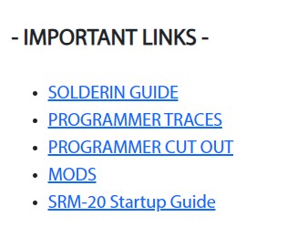
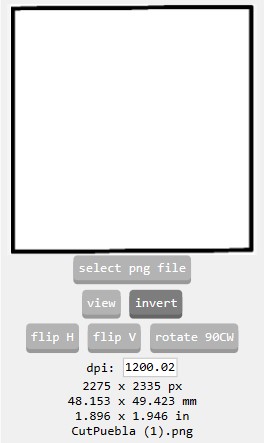
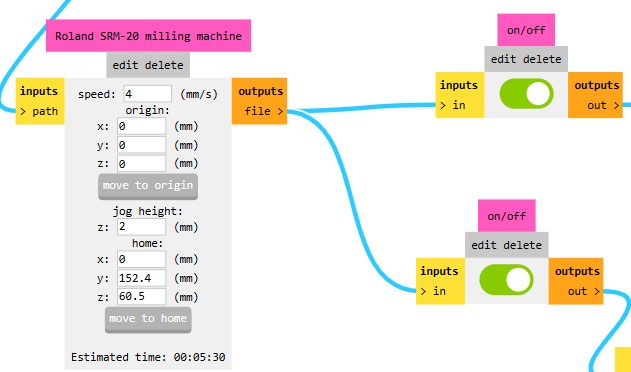
For the design of the electronic board, we used a ready-made design. On the group assignment page are some links. The one I used is the MODS link to prepare the designs.
When we open "MODS" it shows us a menu where we select programns.
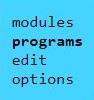
Then we select the option open program.

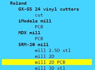
Then we select the option of the image.
It will send us to another page where we will see the following:
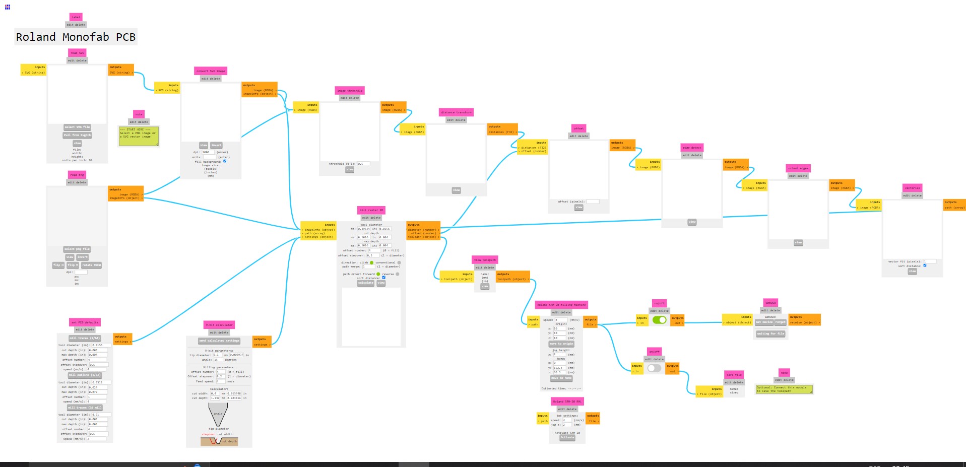
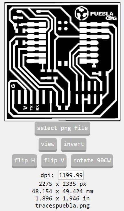
Select the first file we downloaded called traces.
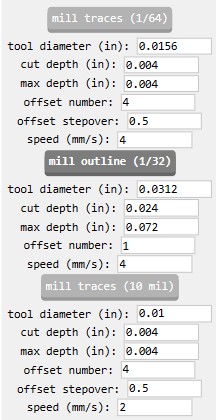
Then select the mill traces (1/64) option.
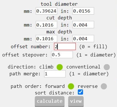
Next, we change the offset number to 2.
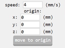
Change the x, y and z values to 0.
Finally, we get the following file in .rml format.
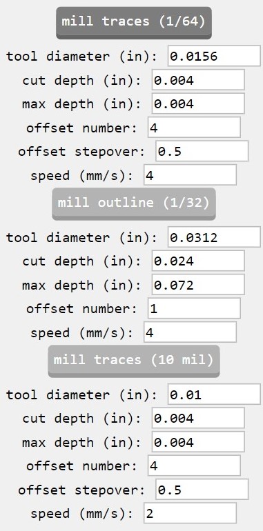
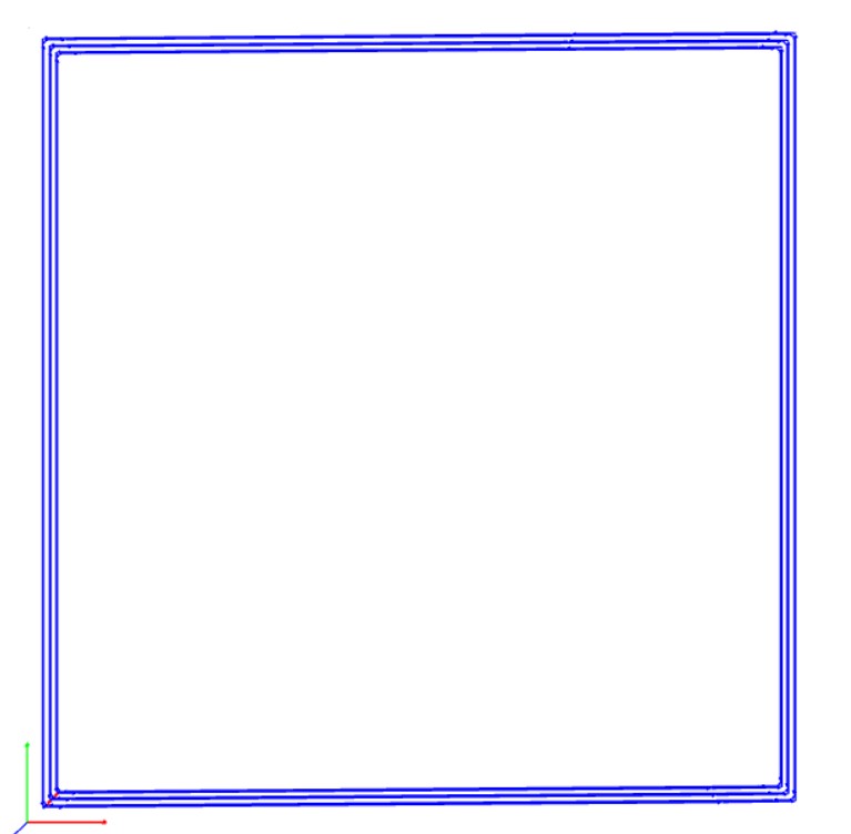
To configurate the second file I follow the next steps:
First, I open the file and I invert it.
Then, I chose the tool to make the cut, in this case I used the tool (1/32).
The difference between the first file and this is the offset number, when we change the tool we can see a new configuration.
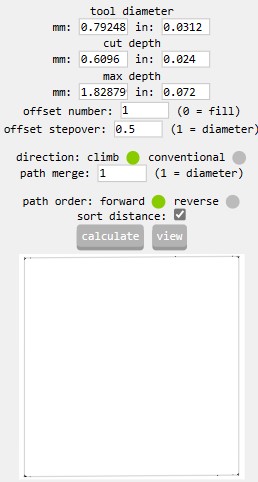
To finish the file I used the same configuration.
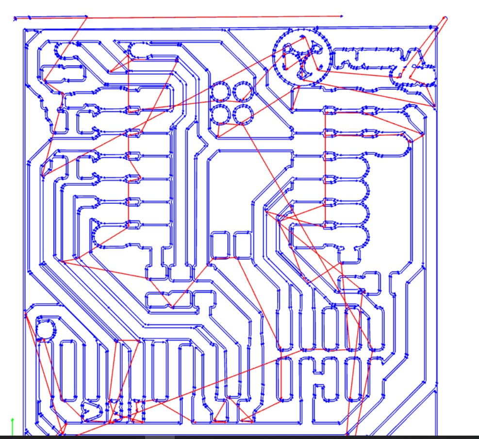
Finally, we obtain the next result:
PCB milling
The machine I used to make my board is the ROLAND SRM-20 model.
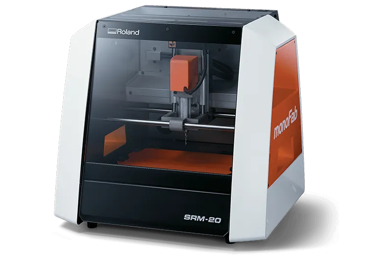
This machine has the following features:
Cutable Material
Modeling Wax, Chemical Wood, Foam, Acrylic, Polyacetal, Acrylonitrile Butadiene Styrene (ABS), Printed Circuit Boards
Operational Travels in X, Y, and Z
203.2 mm (X) × 152.4 mm (Y) × 60.5 mm (Z)
Loadable Workpiece Weight
2 kg
Operation Speed
From 6 mm/min to 1,800 mm/min
Software Resolution
0.01 mm/step (RML-1), 0.001 mm/step (NC Code)
Mechanical Resolution
0.000998594 mm/step
Spindle Rotation Speed
Adjustable from 3,000 RPM to 7,000 RPM
Interface
USB
Operational Noise
During operation: 65 dB(A)
External Dimensions
451 mm (width) × 426.6 mm (depth) × 426.2 mm (height) (17.76 in [width] × 16.80 in [depth] × 16.78 in [height])
Weight
19.6 kg
PCB development on PCB Milling
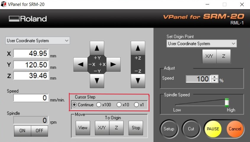
To start with the etching of the board, we open the PCB Milling software called VPanel for SRM-20.
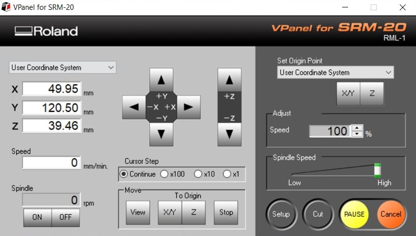
To start we turn on the machine and connect the machine to my computer.
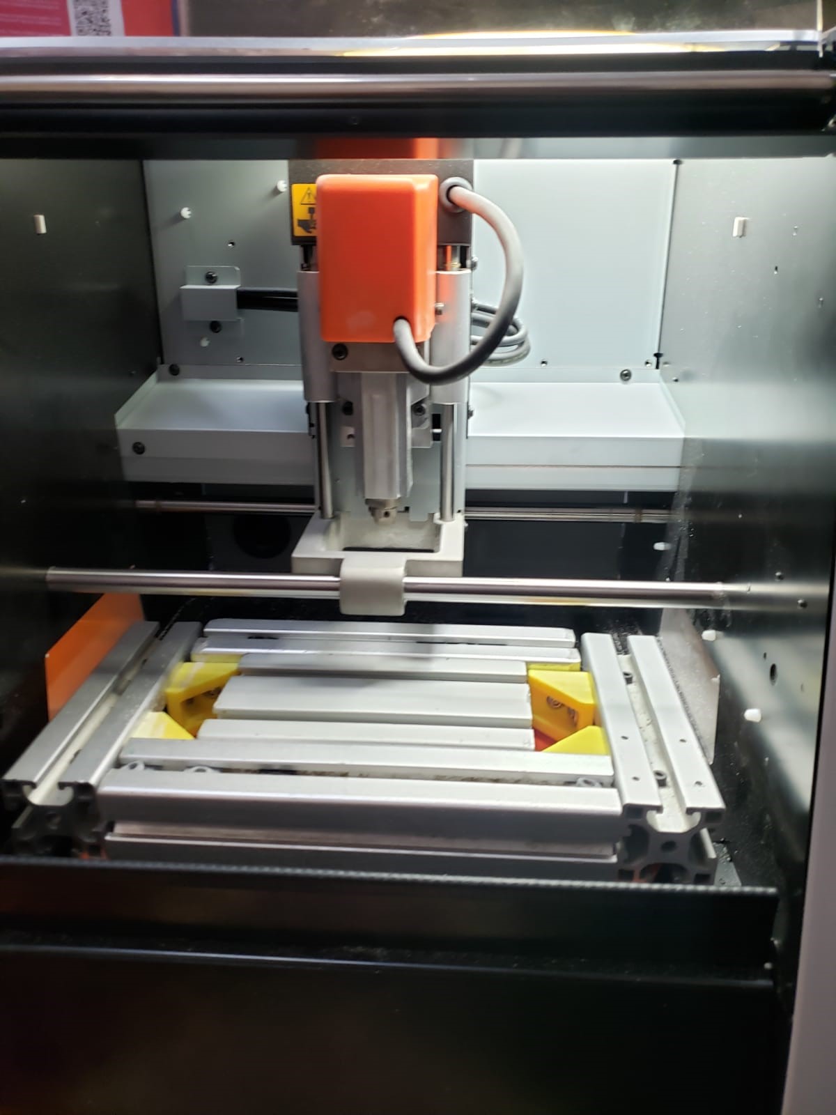
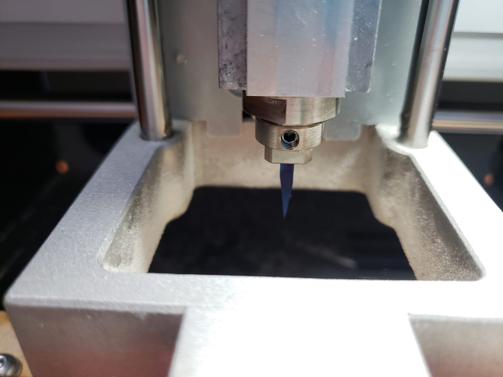
We put the cutting tool that is not flattened at the tip.
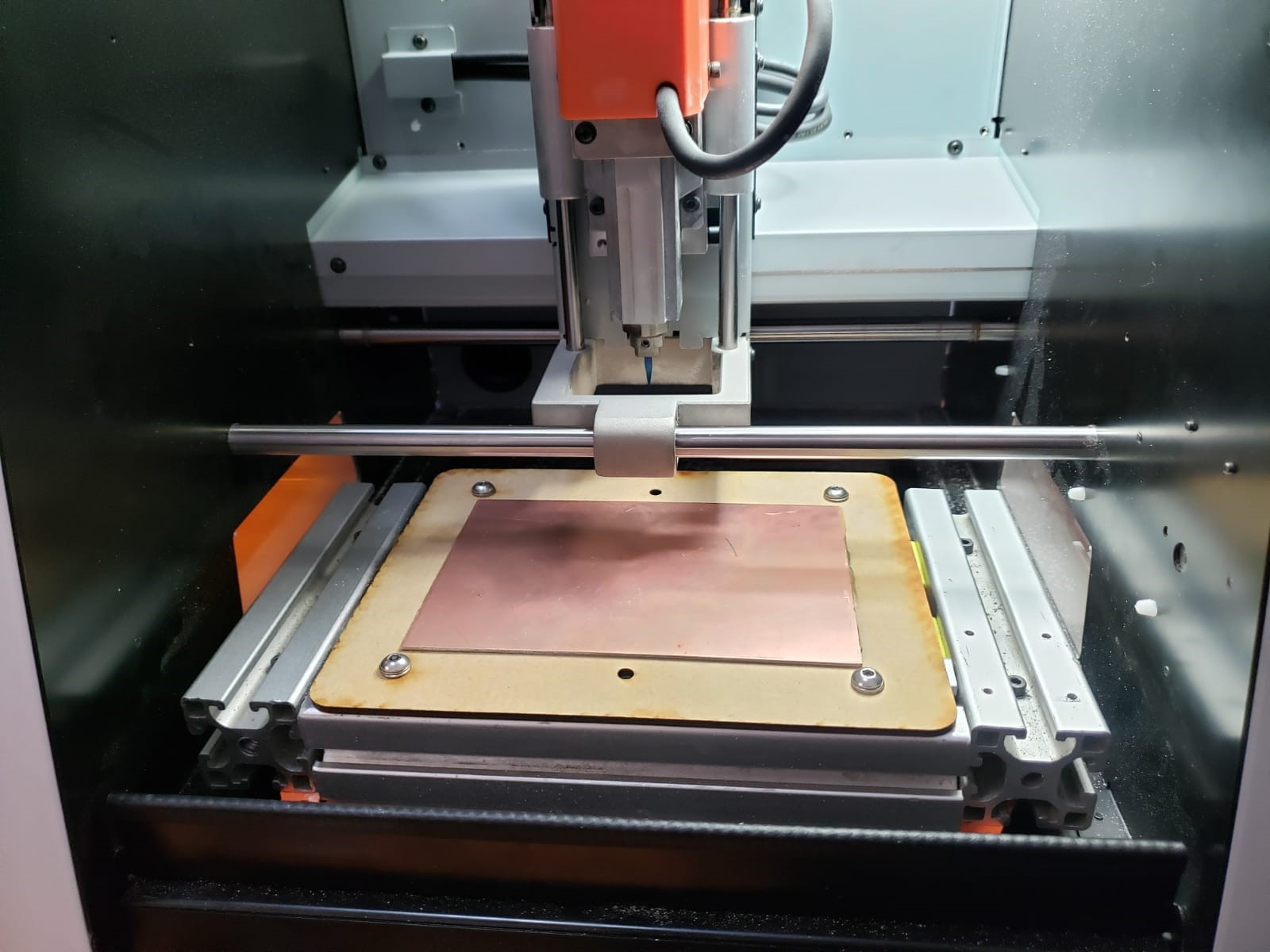
Then, we adjust the "sacrificial board" with the copper board already glued.
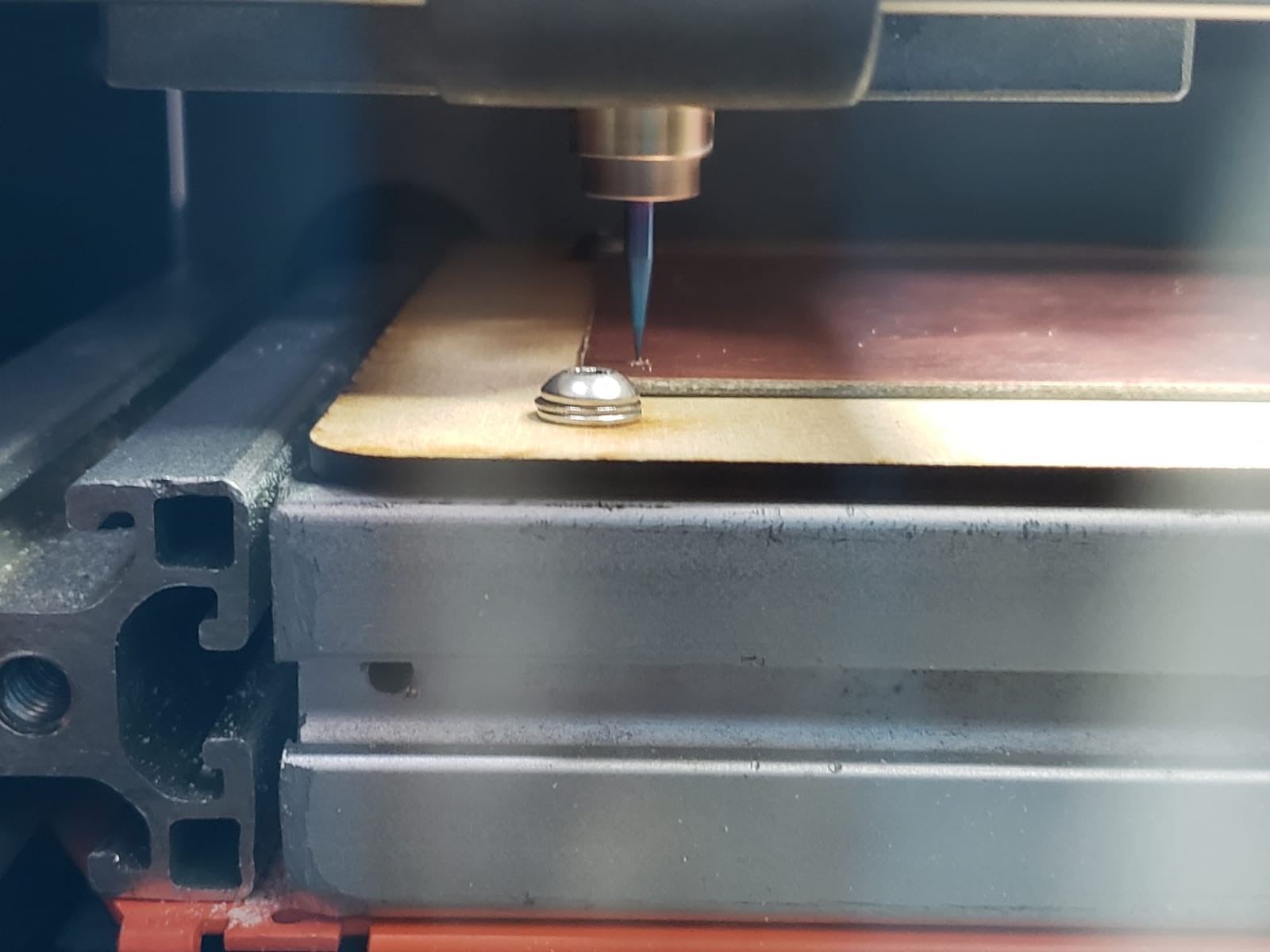
Then we adjust the tip on one of the corners of the copper board. We use the arrows to move on the x and y axis. And to move down we use the arrows on the z-axis.
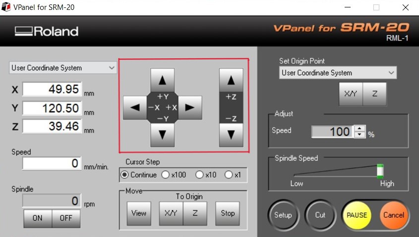
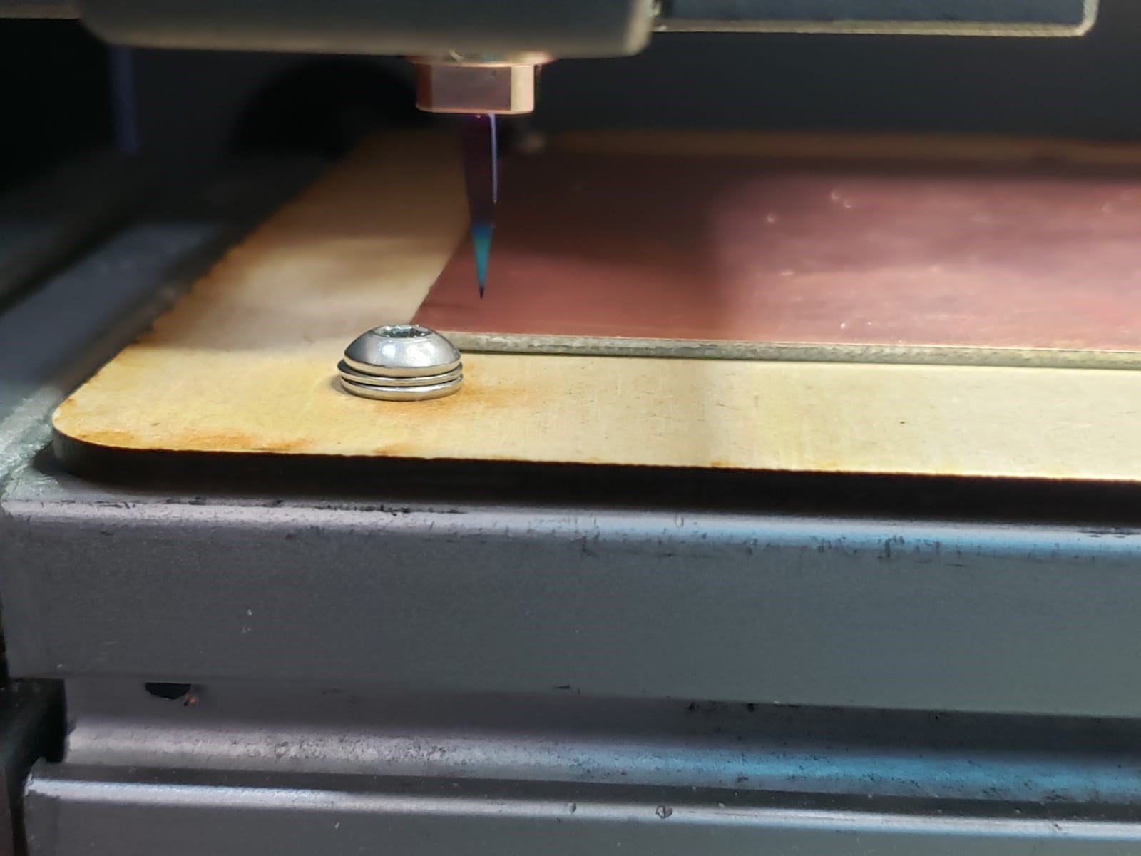
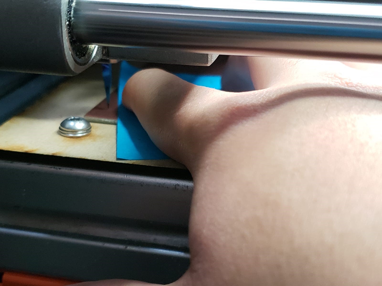
Then, using a piece of paper to adjust the z-axis, we carefully go down using the cursor step x100 and x10.
We lower until the paper can't come out.
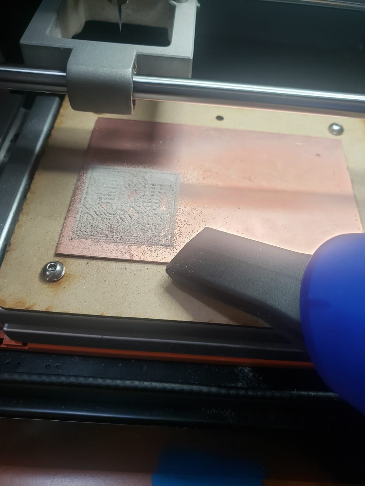
Select the first file in the Cut option and the engraving starts.
At the end, we remove the residues with a vacuum cleaner.
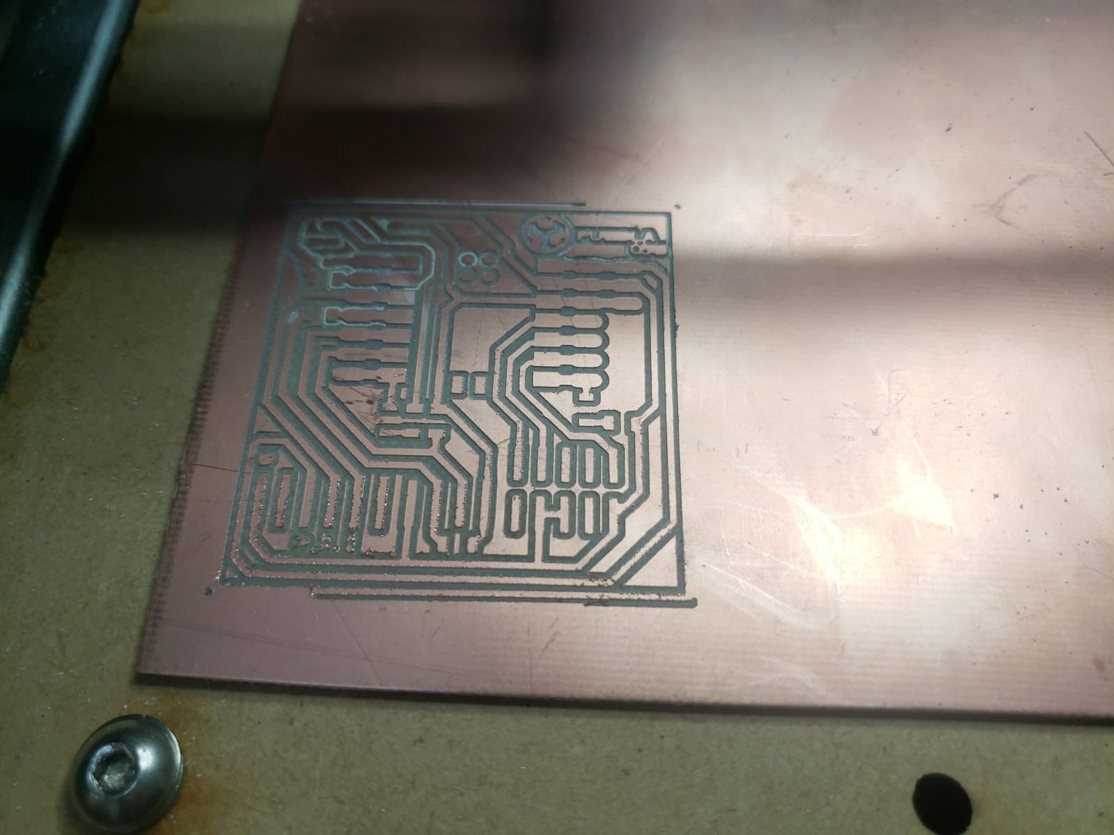
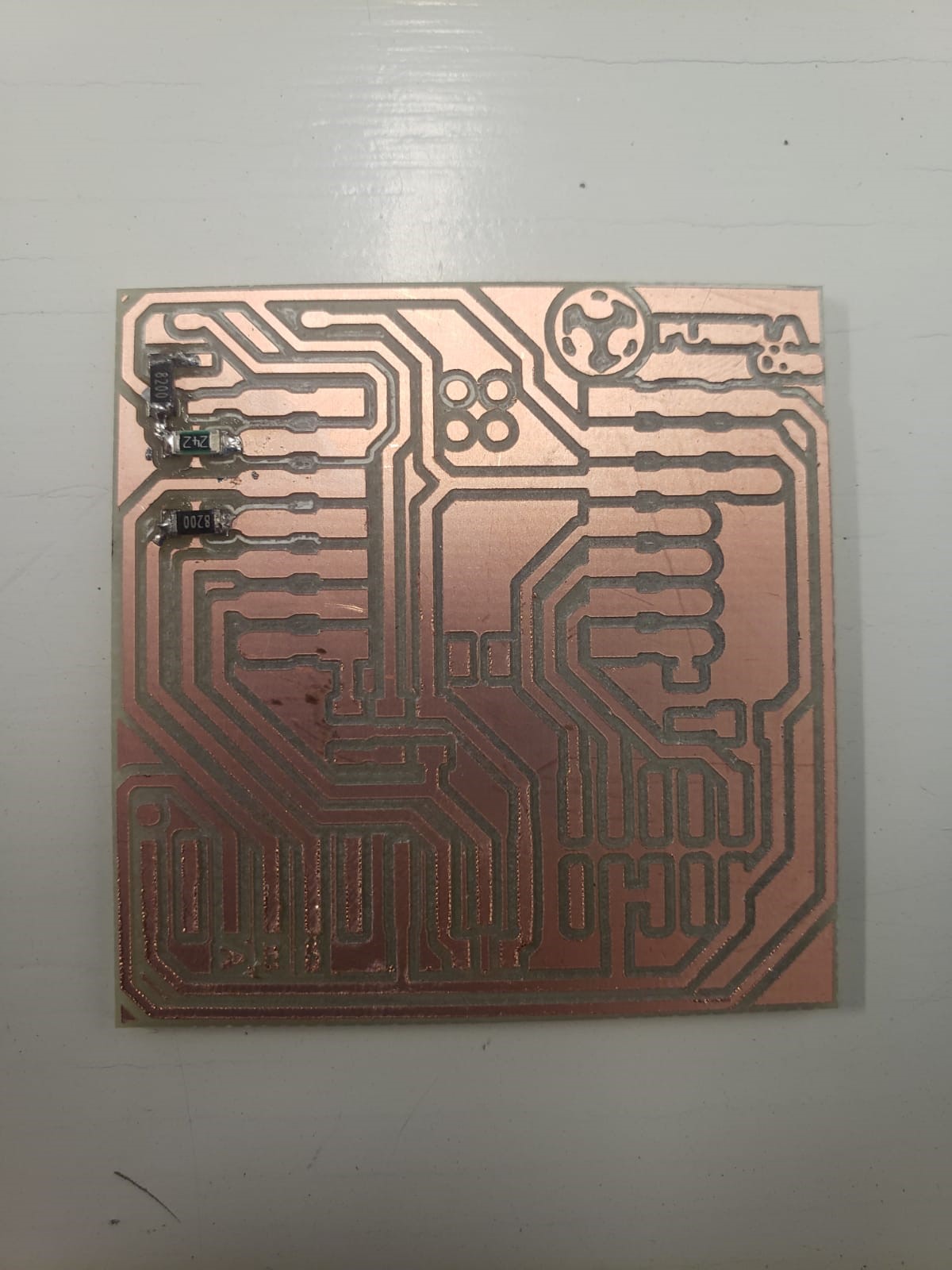
The result of the engraving is as follows:
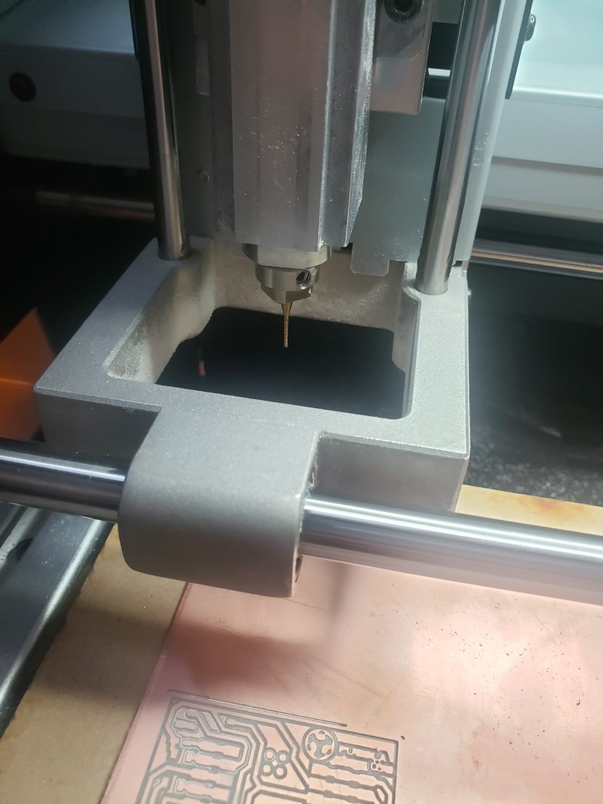
Then, we change the drill bit. We adjust the origin again using the arrows. And we start the engraving of the second file.
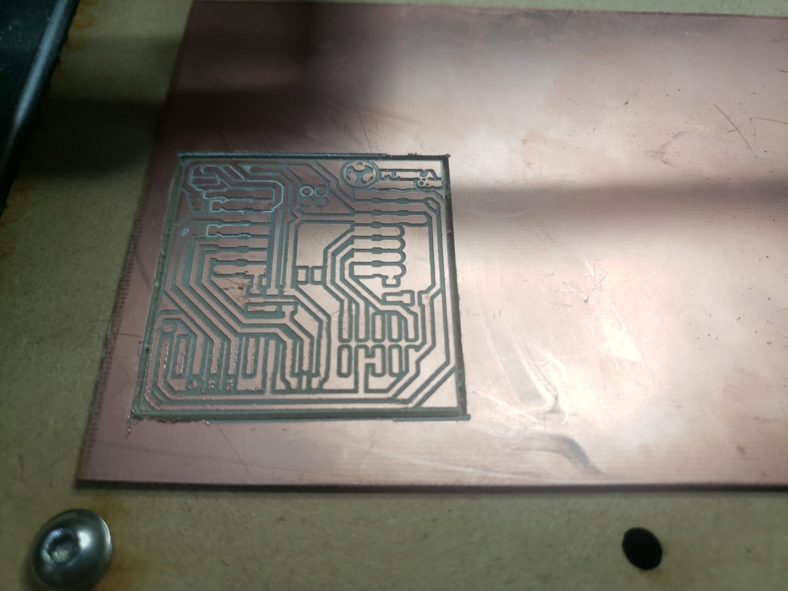
The final engraving on the board is as follows:
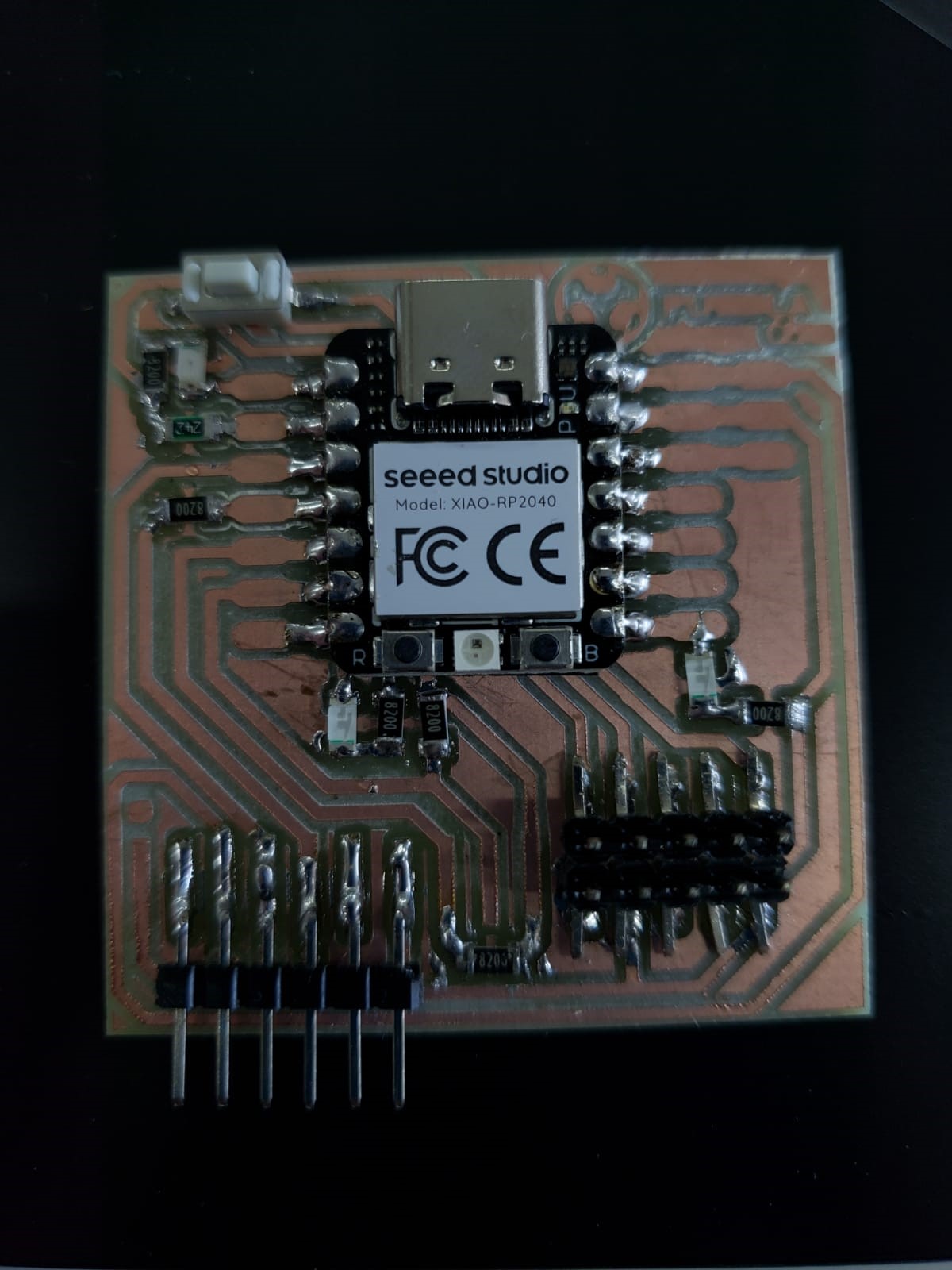
Soldering the components on the PCB
Components
Microcontroller
Xiao-Rp2040
Micro leds
Three leds
R820E-1206 SMD Surface Resistor
Six resistors
Resistor SMD RR0816P-242-B-T5
One resistor
Buttons
One button
Pins
Sixteen pins
SMD Resistor “R820E-1206”
Resistance Value: 0.82 ohms
Package Size: 1206, which measures approximately 3.2 mm x 1.6 mm
Maximum Power: Generally between 0.25 watts to 0.5 watts
SMD Resistor “RR0816P-242-B-T5”
Resistance Value: 2.4 kiloohm
Package Size: 0816, approximately 2 mm x 1.6 mm
Tolerance: ±0.1%, indicating high accuracy
The soldering process was complicated for me. I had never done it before. So I decided to practice before soldering the main board.
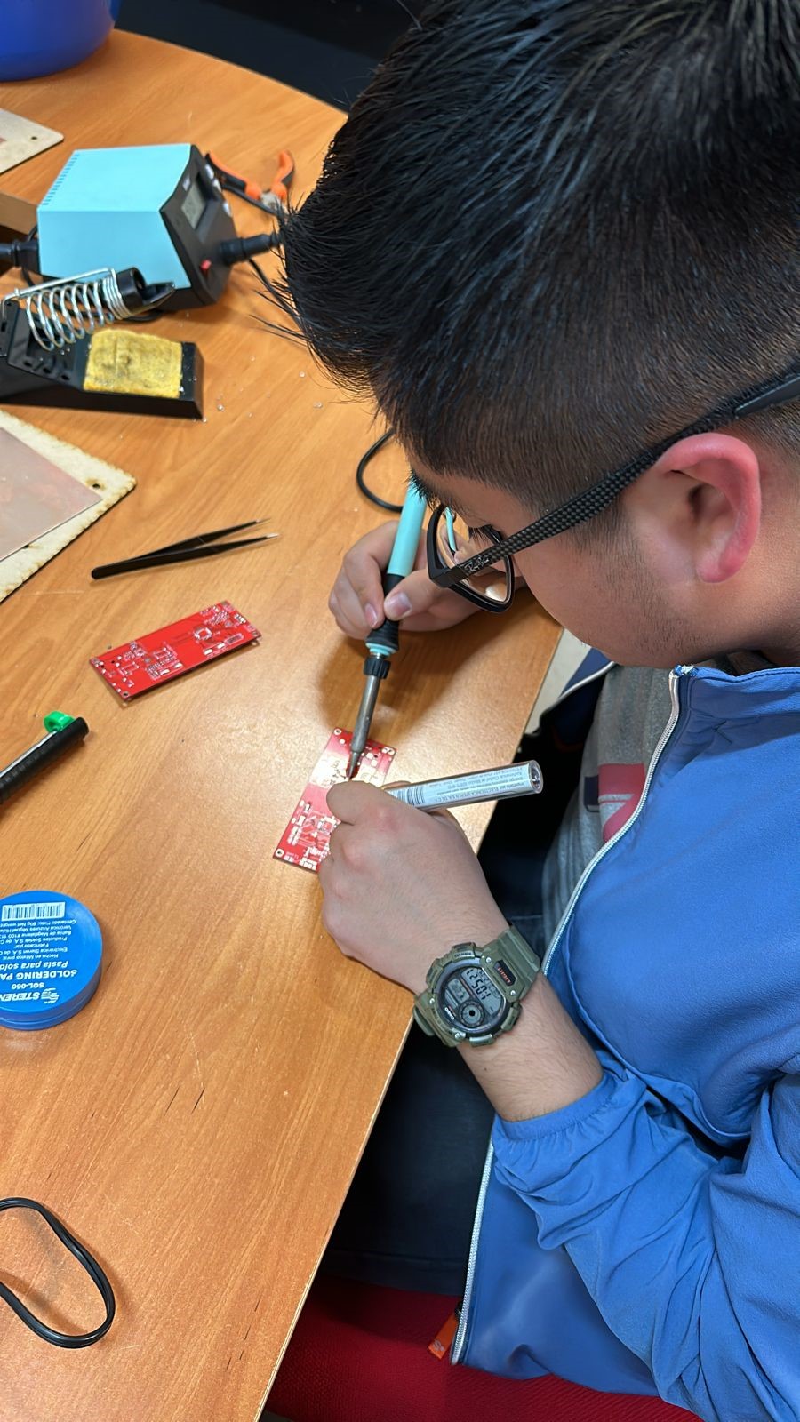
After some practice I started soldering. I started with resistors and leds, which are the smallest components.
The result of my first time welding is as follows:
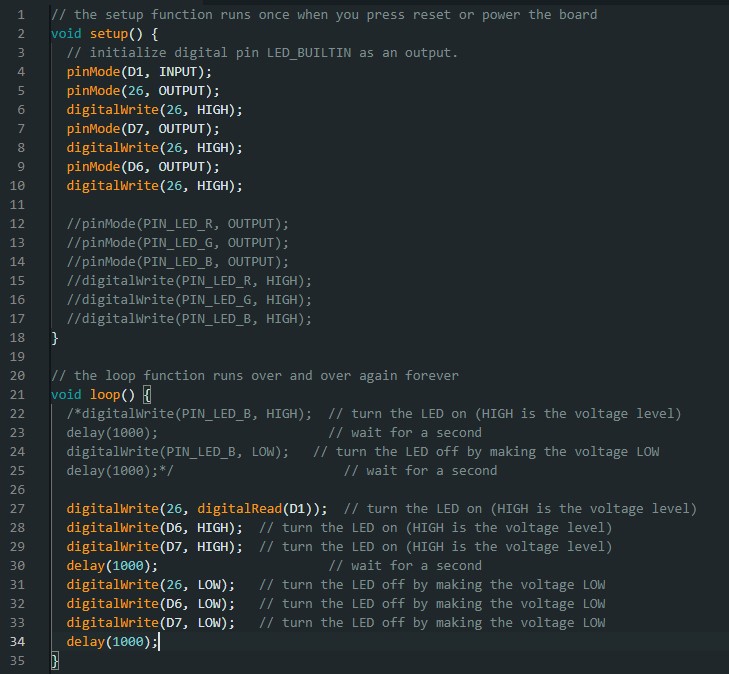
Check that the board works
To check that the PCB is well done, I used the following code. Basically what it does is to turn on two LEDs in a loop, and the third LED turns on when I press the button.