

Electronic Design
Electronic design includes the process of idealising, prototyping, and refining electronic circuits and systems. It involves the integration of components such as resistors, capacitors, transistors, and microprocessors to create devices That will be used for day to day activity.
In the realm of electrical circuit design, several software tools are indispensable for engineers and designers, streamlining the process from concept to realization. Some of them are:
- Altium Designer
- Kicad
- Autodesk fusion Electronic
- live wire
Group Assignment
The Kannai team as usual was divided into two and i worked with Ahmad Tijjani Ishaq The task is to use the test equipment in your lab to observe the operation of a microcontroller circuit board and our documentation can be found in Our group assignment page
Individual Assignment
NOTE
All source files can be found Here at the side bar. For indepth reference we can consult Fusion electronics page kannai reference
Assignment for the week is to use an EDA tool to design a development board to interact and communicate with an embedded microcontroller, produce it, and test it
I designed and Produced my final Project electronic board and to do that i follow the following processes:
- Design
- Preparation of Milling Data
- Milling Operation
- Post milling processing
- Soldering
- testing
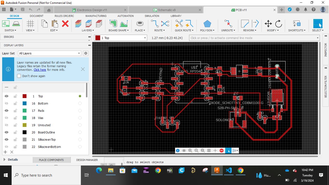
Design
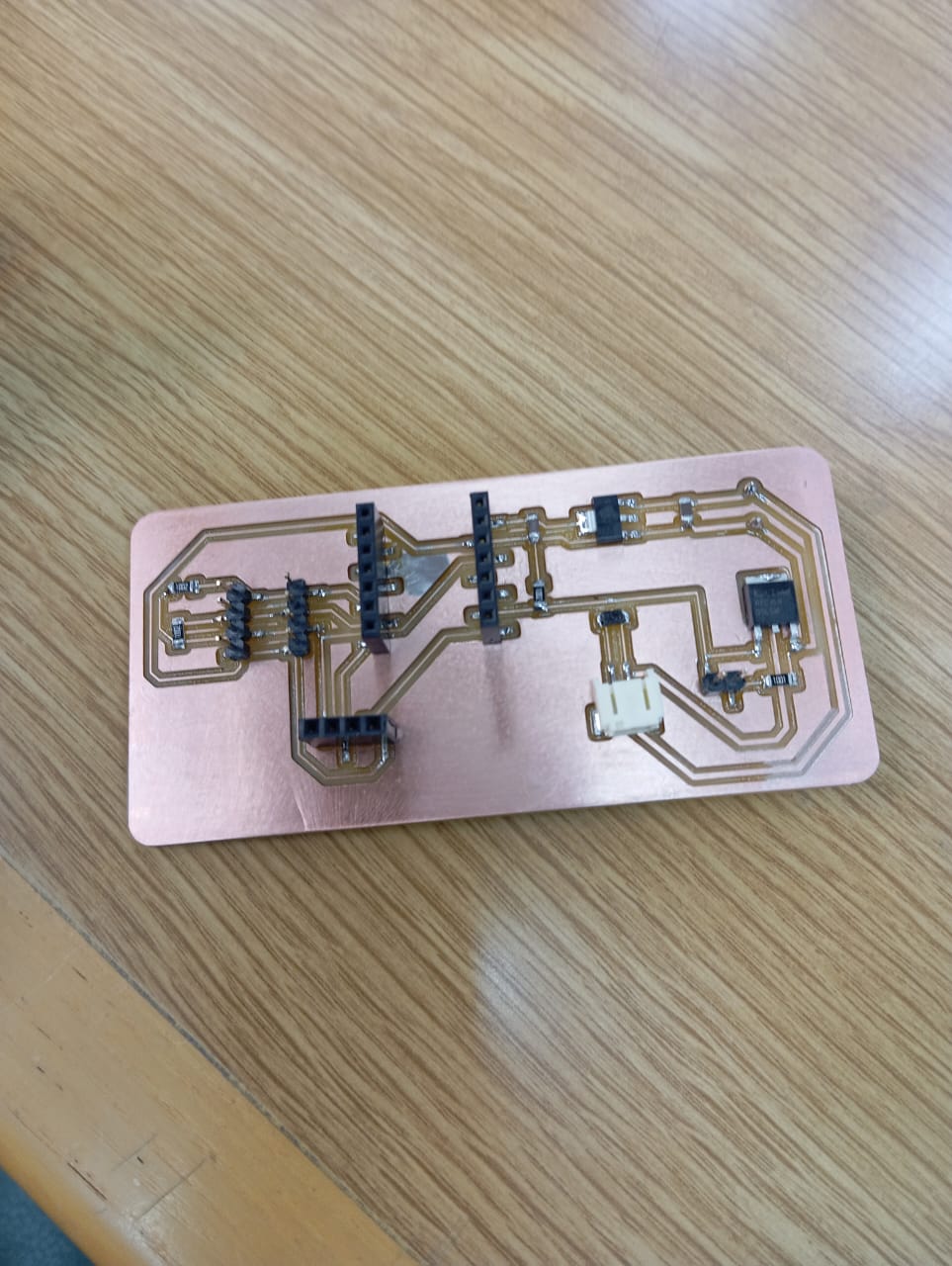
I made two boards for my final project.
Board 1
I am very used to Altium Designer, I decided to try my hands on Autodesk fusion 360 electronics to increase my versatility
and enhance my design options.
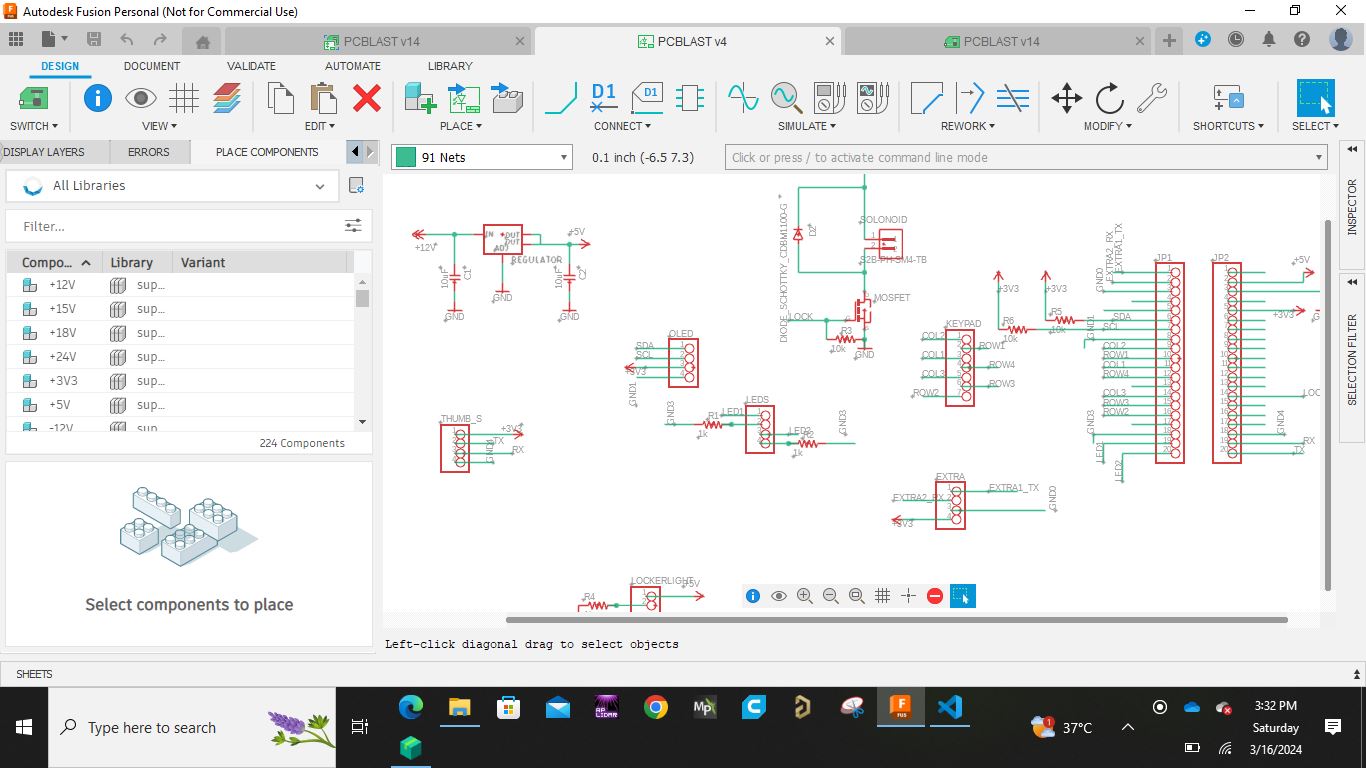
I was introduced to it by my Local Instructor Yuich Tamiya and i really enjoyed using it. I follow the following processes to do my design.
For indepth reference we can consult Fusion electronics page kannai reference
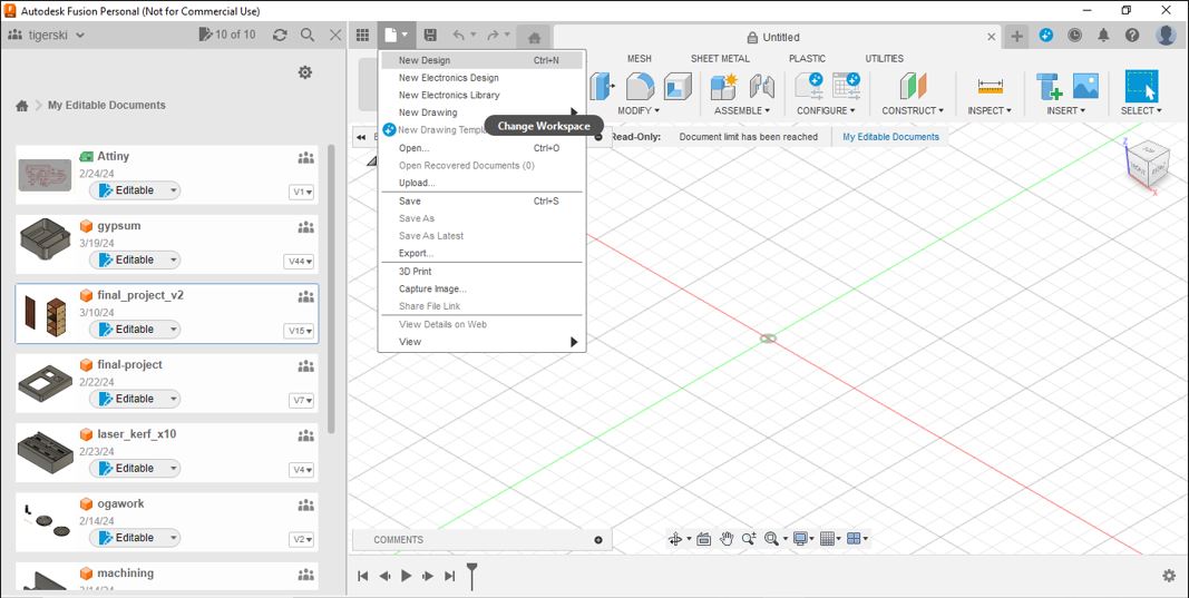
- I started by creating a new electronic design
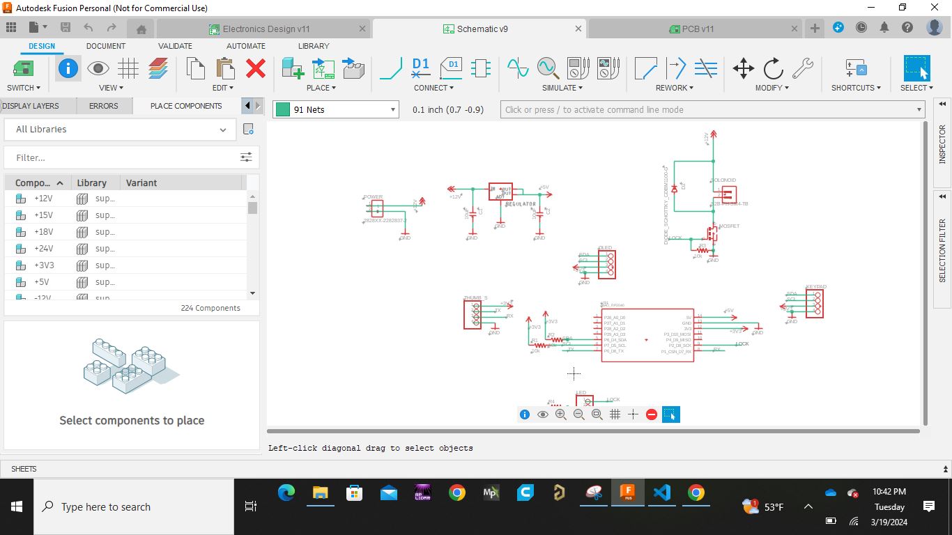
- I then opened the schematic and started adding components from the components library based on my design. To add components one has to input "add" into the command line. Fusion electronics have so many command used for design processes.
- for components that are not available i download their footprint and schematic from SNAPEDA website
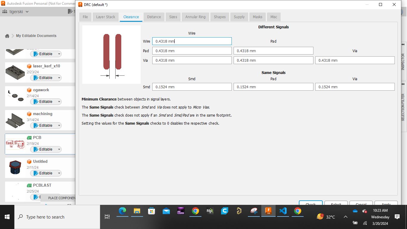
- I set up my DRC (design rule)
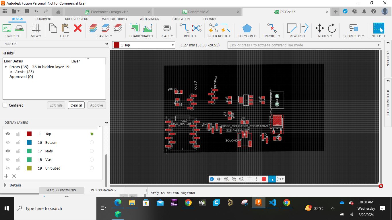
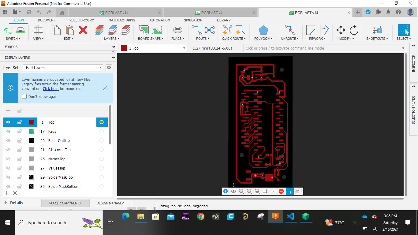
- I then transfer to pcb
- I did the routing and with routing completed i then exported my top layer, Pads layer, and outline trace as png images


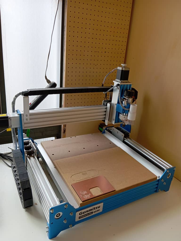
Preparation of milling Data
For data preparation i used mods website, Explanation
on how to use mods properly can be found in my electronic production week
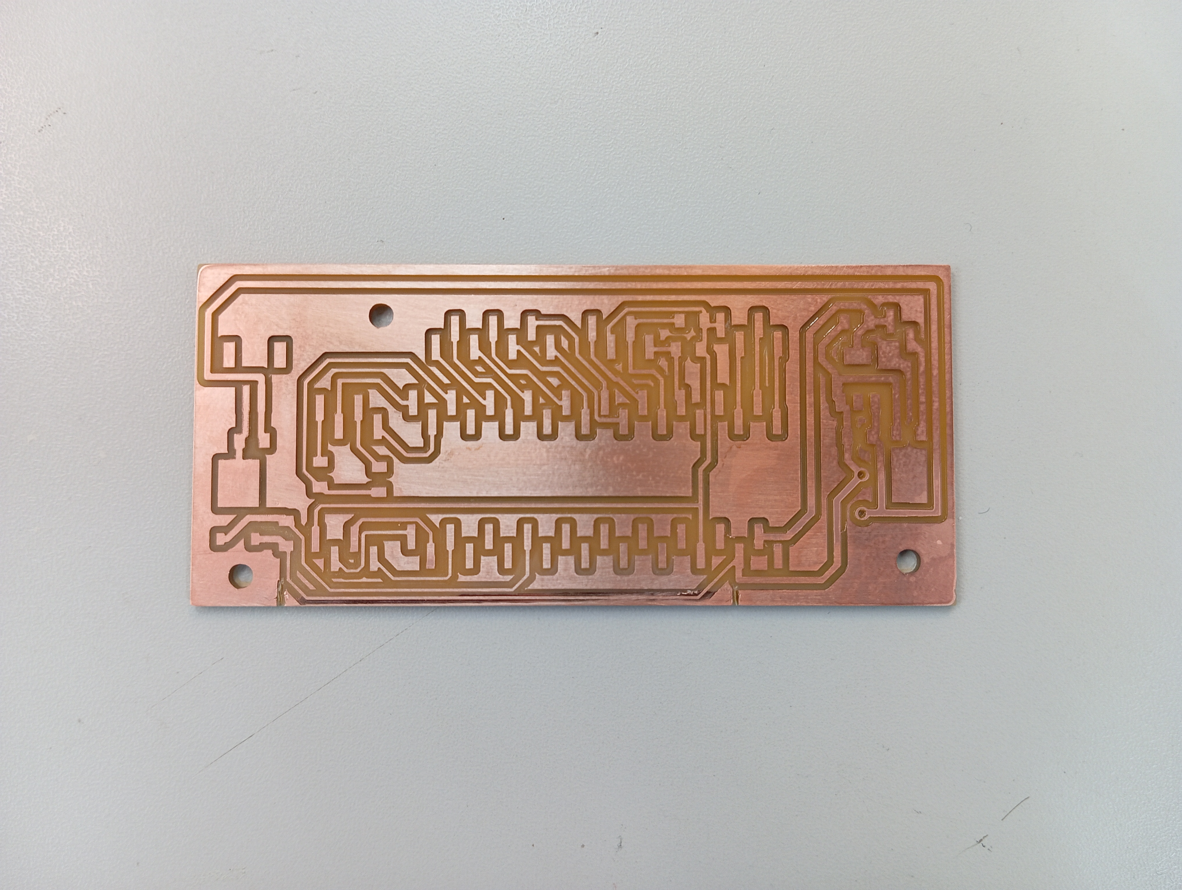
After obtaining my data i proceed to cut mill the board.

Milling
I used the genmitsu cnc to mill my board with the help of Gsender software, you can refer to my week 4 electronics production page for indepth on the use of the cnc machine.


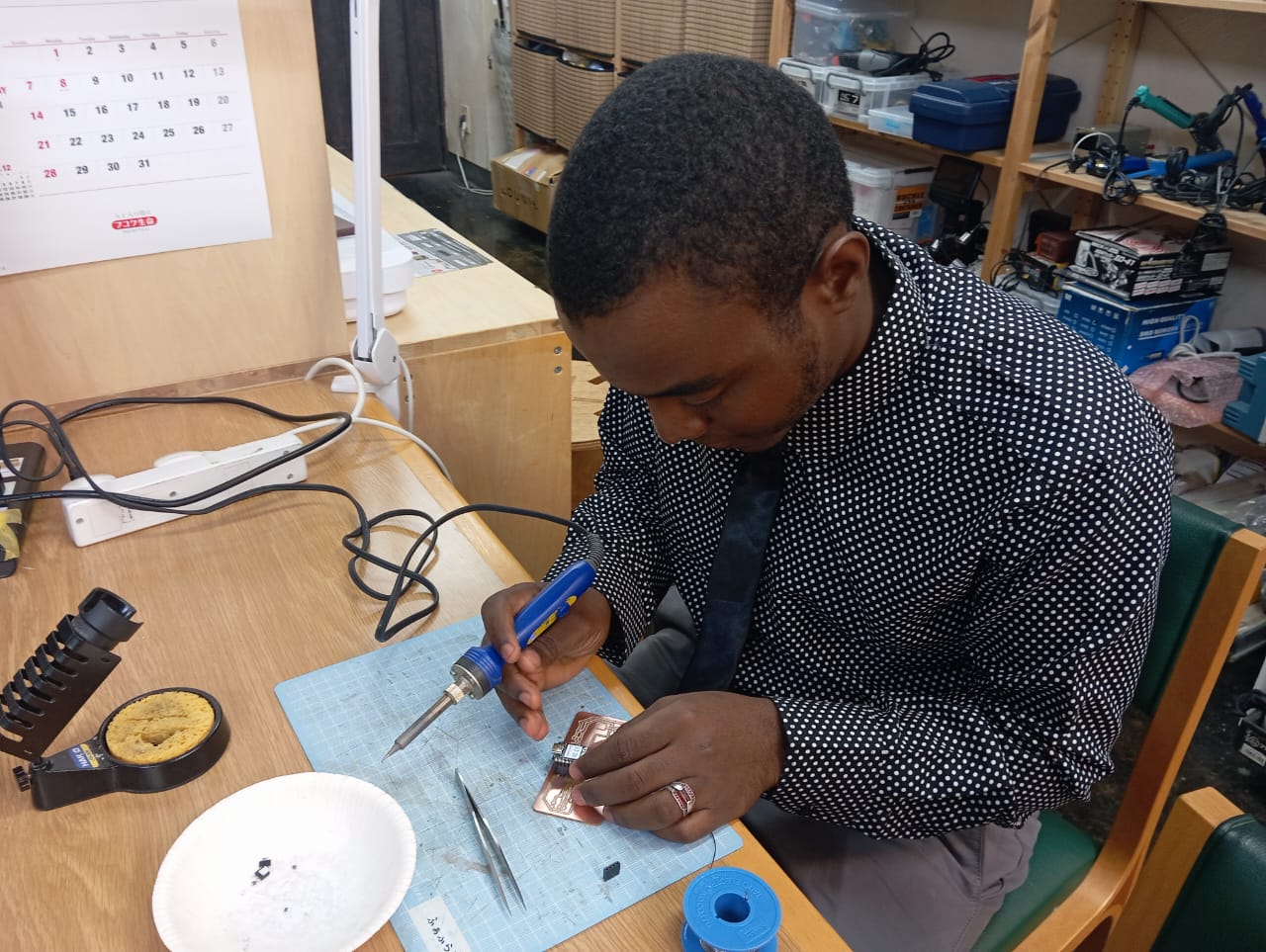
Soldering
I did soldering for my board, i soldered all the components.
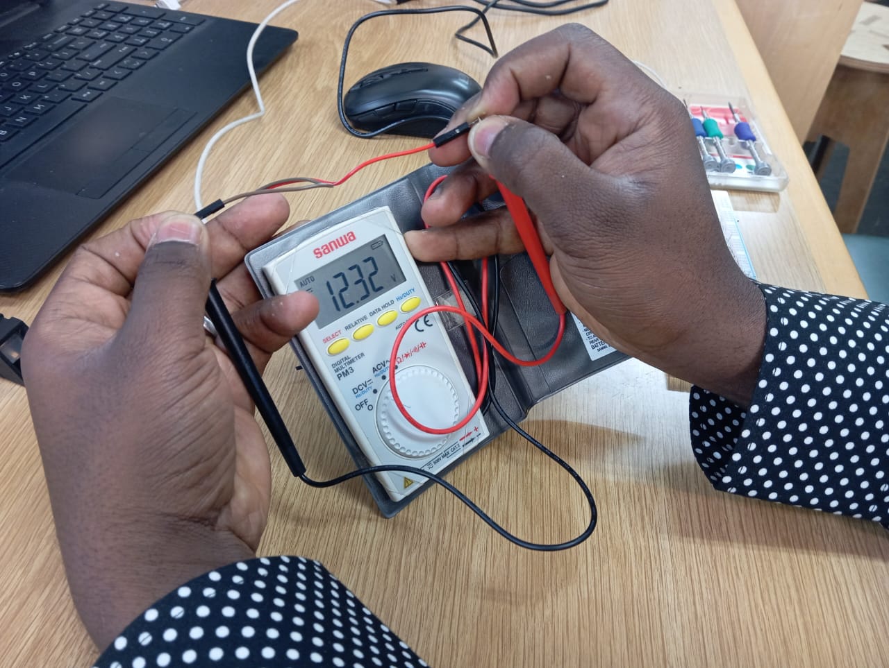
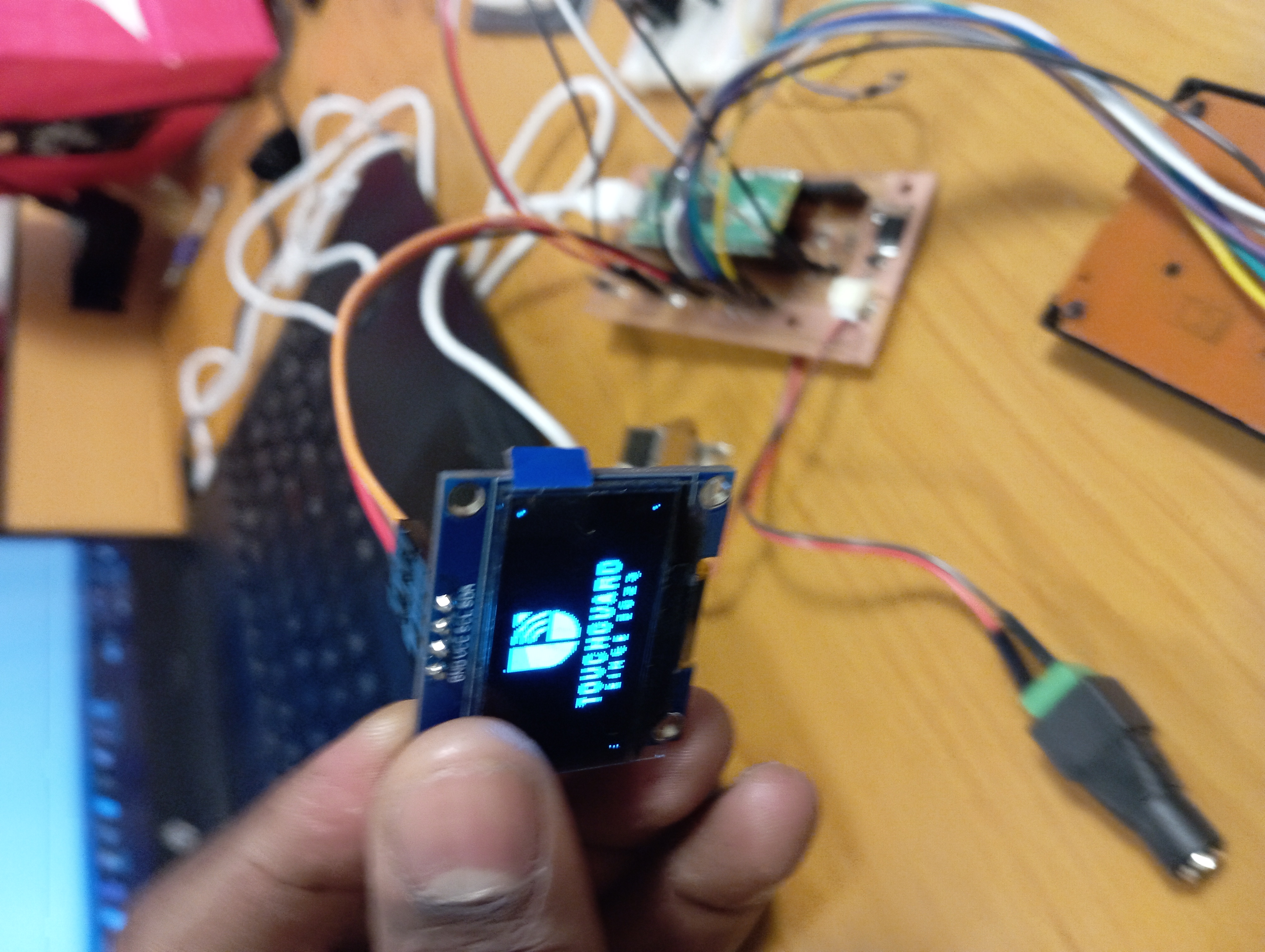
TESTING
Board 2
My final project requires a lot of pins than xiao seed studio can provide, hence i made another one with pi pico. The processes are similar as above and the snap shots are shown below.
Design
Milled Board
Testing
All source files can be found Here at the side bar.