8. Electronics Design
This week we were tasked individually to use and EDA tool to design a deveolopment board, produce it, and test it. For my EDA tool, I used KiCad.
Group Assignment
Our group assignment for this week can be found here
KiCad
To start out, I added the KiCad footprints and symbols from the fab library. I did this by cloning the repository using SSH and went into KiCad. I went into the “Manage Symbol Libraray” from the Preferences tab and added the fab.kicad_sym file into it by pressing the folder button and finding the repository and file.
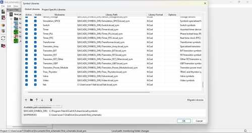
I then did this for the footprints as well by going into “Manage Footprint Libraries” and adding the fab.pretty file into it.

I then started a new project and named it fab_week8_projects.
I wanted my circuit to have an LED indicator for whenever the board it powered on, an LED that I can program along with a button. The board will be able to do with what i did with my Quenntorres in Week 4.
Schematics
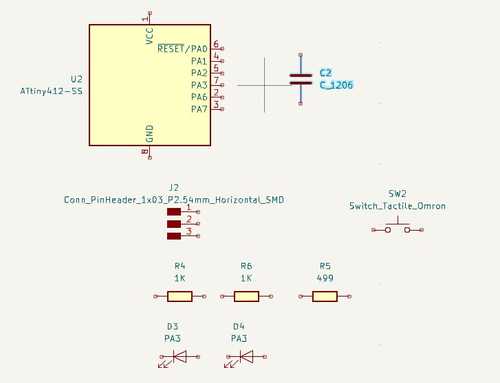
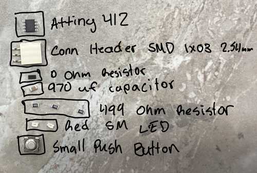
The first thing I did was add all of the components I would need. That being an ATTINY412, capacitor, 1x3 Conn Header 2.54 Horizontal_SMD, Tactile Switch, 3 resistors, and 2 LEDs.
These could be added in the Schematic Editor by utilizing the Add Symbol tool. This opens up all of the symbols and their partnering footprints for the PCB Editor in a list. For things like the ATTINY412 and Tactile Switch, they are all already installed when you install KiCad. But for everything else, the symbols and footprints I needed were only there once I added them from the fab library. These are all of my components laid out
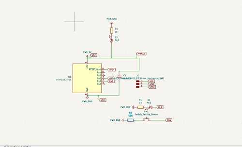
The process of wiring the schematic was a process of trial and error. A lot of scrapped desings were created in the process of making the circuit I wanted to create. Most of them stemmed from a lack of organization with my Schematic Editor which made it hard to figure out where exactly my traces were supposed to go in the PCB Editor. In this video of this weeks Global Open Time, Adrian Torres showed a method of wiring that I was not applying to my schematics. That being the “Global Labels” which is a tool that can be accessed on the right side of the schematic editor. This helped my organization a lot. The Global Label tool allows you to create a label that can be called upon when wiring components. This can be used to automatically wire things without having to use the wire tool to move around your design and wire manually.This helped a lot with my organization. This is my almost finished schematic in my schematic editor.
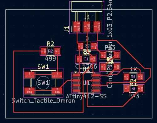
Once everything was laid out nicely, I went into the PCB Editor and updated my PCB from Schematic. I then reorganized the parts and used the Route Tracks tool to add the traces for the PCB. I then went under the “Edge Cuts” layer which is were you define the edge of your PCB and then made a rectangle around all my components. This is my finished PCB in my PCB editor.

I realized that the trace that connected my LED indicator to my power was connecting with the other spots of the Conn Header. I went through this way because there was no other way for the trace to go because it was trapped inside the other traces. I fixed this issue by adding a 0 Ohm resistor that jumped over a trace toward the VCC. This is my complete pcb board in the pcb editor.
This is it in a 3D view that KiCad provides under the “View” tab.

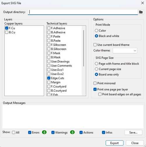
I then exported this as an svg. These are the settings that I used to export my schematic.
Exporting
To turn this SVG into GCode, I went to modsprojects and used the Othermill/Bantam Tools PCB program because I was going to use an Othermill to mill out my PCB. I first started by inserting the SVG, inverting it.

I then calculated the GCode utilizing the PCB traces 1/64 default in the Othermill defaults and mill 2D raster.
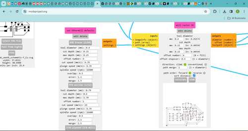
I then made sure this slider was turned on so that the gcode would download automatically.

I repeated this process for the Edge Cuts but I used the PCB outline 1/32 default instead in the othermill defaults. I now had both of my schematics in gcode and ready to mill.
I realized later though that this was a mistake. Using this method made it so that I could not define the trace settings for the milling. I also didn’t make my traces larger in KiCad so they were very skinny and broke easily.

I realized that I needed to export them as gerber files utilizing the Fabrication Outputs. This made it so that I can edit trace settings in the Bantam Tools software. This is the settings I used for my gerber export.

This is my completely milled out board

Soldering
I then soldered my board. These are my components.
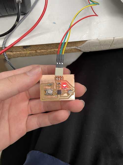
This is my board completely soldered.

Programming
I used my Quenntorres to code my Attiny412 along with the converter from week 6. When I plugged everything in, the LED indicator turned on like it was supposed to.
I then ran a simple blink code on the pin 4 LED and it worked!
Downloads
My downloads for this week can be found here
Reflection
This week was an important one. Designing a PCB board is a very helpful skill that will pull me away from doing wiring with bread boards which makes everything look nicer and clean. I found the inital process of designing the pcb board to be frustrating but once you got the hang of it, it was much easier.