9. Electronics Design
This week I learned how to use various EDA tools to design a development board that can communicate with an embedded microcontroller. You can access all of my files here.
Assignment
group assignment:
-
use the test equipment in your lab to observe the operation of a microcontroller circuit board
-
send a PCB out to a board house
individual assignment:
-
use an EDA tool to design a development board to interact and communicate with an embedded microcontroller, produce it, and test it
-
extra credit: try another design workflow
-
extra credit: design a case for it
-
extra credit: simulate its operation
KiCad
KiCad Tutorial
Firstly, I downloaded the Seeeduino XIAO KiCad library and imported it into KiCad by going from preferences>manage symbol libraries>project specific libraries. I selected Legacy as the library format and inserted the .lib file under library path.
Then, I followed this tutorial series, which explained the basic features of KiCad, how to run DRCs and ERCs, add footprints, and produce a Gerber file. I liked following these tutorials because a lot of the errors/warnings I ran into during the DRCs/ERCs were different than the ones he had, and it allowed me to troubleshoot on my own. The downside, however. is that some of the details in his circuit go unexplained, which made it slightly harder to follow.
After opening up the schematic workspace, I used the add symbol feature to insert components, followed by connecting them to the ATtiny85 with wires.
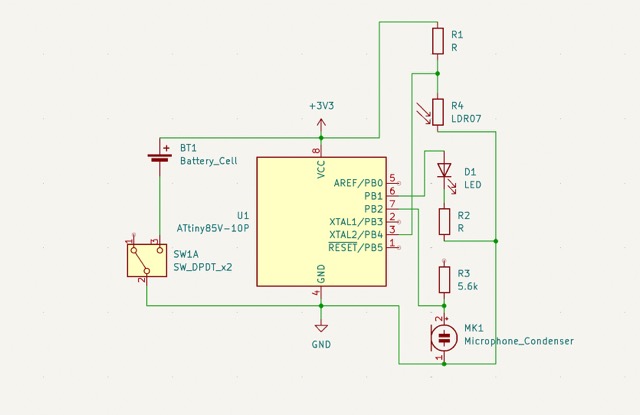
This schematic was a bit messy in terms of component placement, so the video recommended using net labels to represent connections without the components physically touching. Additionally, he used the text feature to designate each unit.
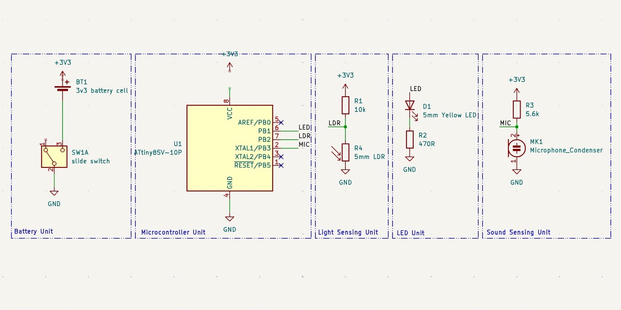
It looks way better now!
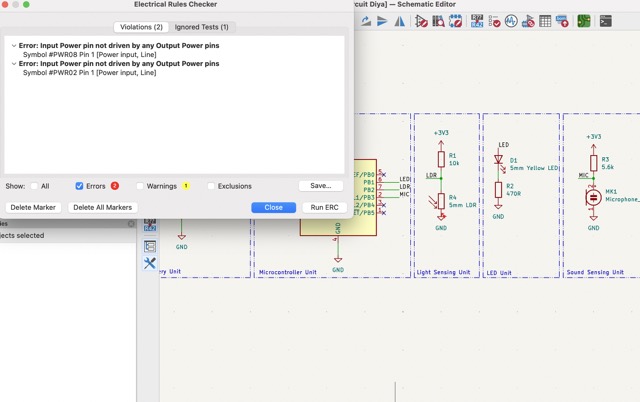
Now that the basic schematic was finished, I could apply the electrical rules checker to ensure that the circuits work as the should. KiCad automatically outlines where these issues are upon clicking, so fixing them was pretty intuitive.
Next, I could assign footprints, which connects each symbol in the schematic to a physical model/component. I opened up the footprint assignment tool, clicked on one of the symbols, applied the filters, and searched for the appropriate component. This was by far the trickiest step, as there was a tremendous amount of models available.
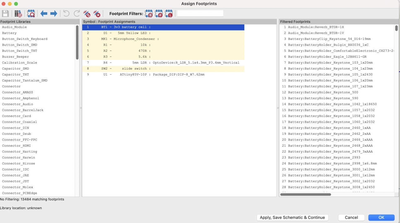
Yellow indicates that a footprint has not been assigned to that symbol yet.
Once footprints are assigned, its time to set up the actual PCB layout with traces! To do this, I went back to the main project menu and opened up the PCB editor. First, I opened up Board Setup>Board Editor Layers to select which layers of my PCB I wanted to include.
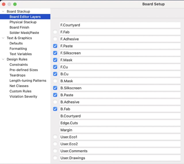
These layers, organized in pairs for front/back, can sound confusing at first, so here’s a little guide to what they mean:
-
F. Courtyard and B. Courtyard defines a safe area around a component so that it doesn’t overlap with another component when assembled physically
-
F. Fab and B. Fab provide additional information to manufacturers
-
F. Adhesive and B. Adhesive is used for components that aren’t easy to mount and require additional glue/material
-
F. Paste and B. Paste indicate where to not apply the solder mask, or where to solder the components
-
Edge cut defines PCB shape and dimension
-
Margin layer defines area where components/traces/etc. are allowed to be placed or not allowed to be placed
For this specific design, I de-selected Fab and Adhesive because they weren’t essential to the file. Then, under Constraints, I followed along with a PCB capabilities chart to determine the minimum clearance, track width, etc. This sets some basic limitations for the design.
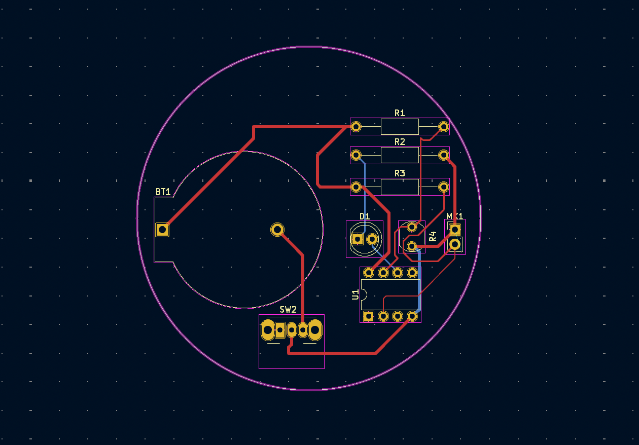
With these settings adjusted, I began my PCB layout! Selecting Edge Cuts under the layers tab, I first created and locked a circular outline for the PCB. I then clicked the Update PCB from Schematic button in the toolbar, selected Update PCB, followed by close. This enables me to place down my footprints onto the workspace.
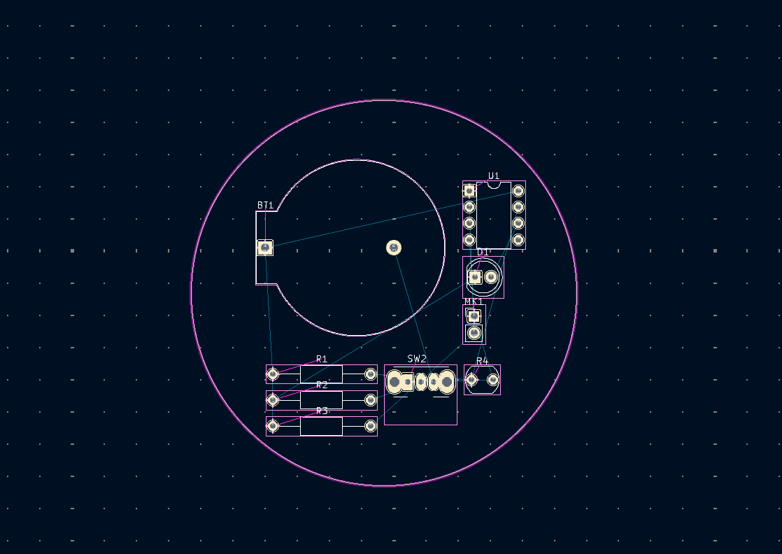
I rearranged the components and drew the trace routes on the F. Cu and B. Cu layers. After running the design rules checker (similar nature to the electrical rules checker), the PCB was finished!
My first attempt at routing the circuit was quite messy as I forgot to consider the constraints I set earlier.
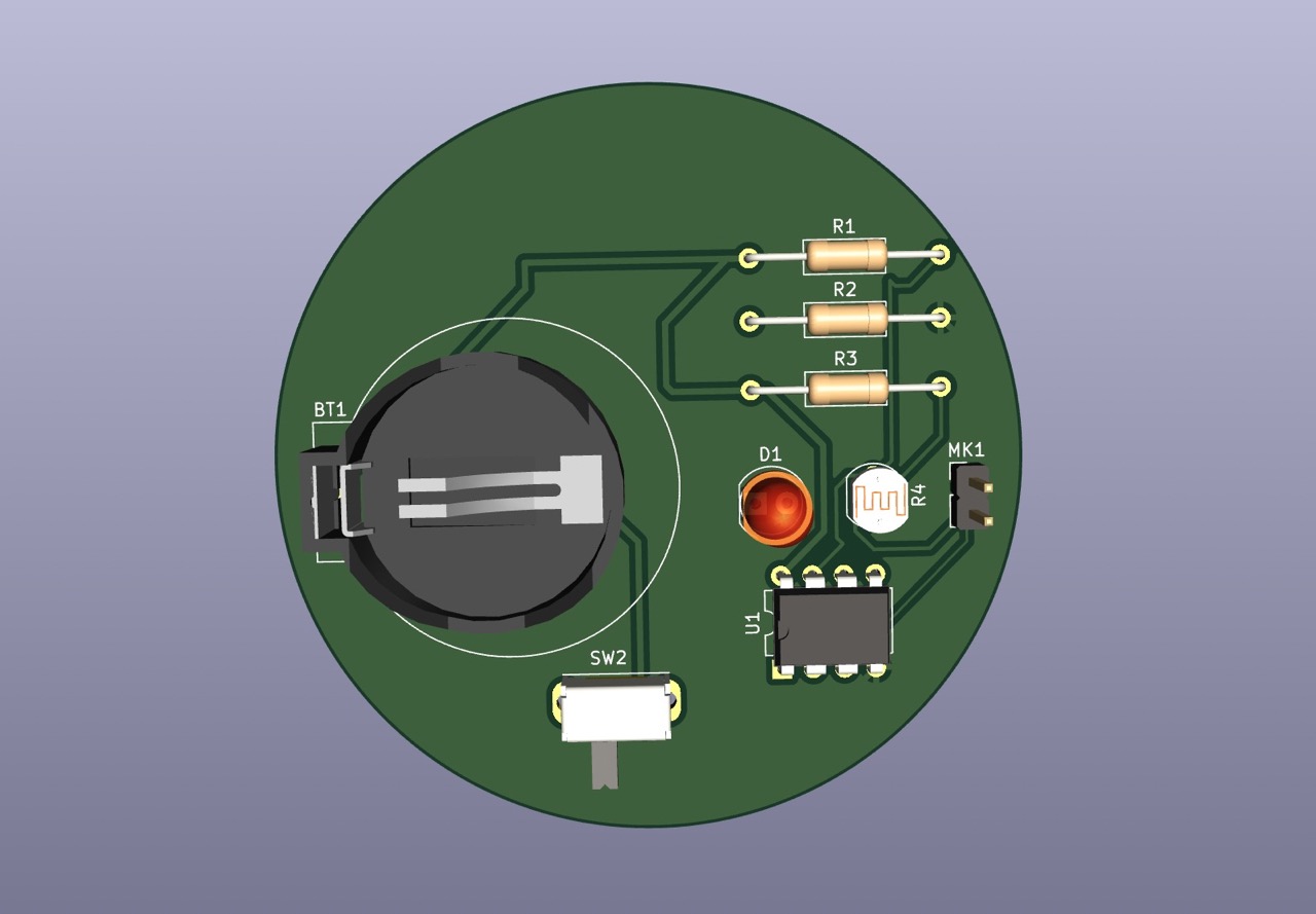
Here is the PCB in 3D (alt + + + 3 to view):
To save the .gbr files, I used the plot command and set the path to a specific folder.
KiCad Cheatsheet
| Icon | Name | Location | Purpose |
|---|---|---|---|
| Add power symbol | Schematic editor | Designates global nets for power connections | |
| Add symbol | Schematic editor | Adds a schematic symbol for a component into the workspace | |
| Net label | Schematic editor | Gives connection without a distinction a specific name (i.e. MIC) | |
| Add net class directive labels | Schematic editor | Creates larger class/arrangement for net labels | |
| Wire | Schematic editor | Electrically connects symbols in the schametic workspace | |
| No connection | Schematic editor | Indicates which symbol pins are purposefully left unconnected | |
| Design rules checker (DRC) and electrical rules checker (ERC) | Schematic editor and PCB layout editor | Evaluates whether the design works as intended | |
| Footprint assignment tool | Schematic editor | Assigns each symbol a physical counterpart called a footprint | |
| Update PCB from schematic | PCB layout editor | Helps in importing all the symbols with footprints into the PCB layout editor | |
| Copper fill | PCB layout editor | Prevents open circuit/short circuits in PCB | |
| Route tracks | PCB layout editor | Creates physical traces for the PCB | |
| Plot | PCB layout editor | Allows users to export the PCB as various files, including Gerber |
Designing an ATtiny412 Blink Board
Now that I had become a bit more familiar with the EDA process and the KiCad, I wanted to try designing my own ATtiny412 blink board that could be used with the QuenTorres, just like the target board I produced during the Embedded programming week. To create this, I first installed this Fab library, which contains a lot of the 1206 components that I will be using. I first started up a new project and opened the schematic editor. Next, I inserted a ATtiny412 chip, a capacitor, a resistor, a tactile switch, an LED, and a 3-pin conn header into the workspace. I built a basic LED circuit that could be activated with a button, and I used the power flag symbol on the VCC and GND pins. I initially had the +3V3 and GND power symbols, but the ERC returned an error.
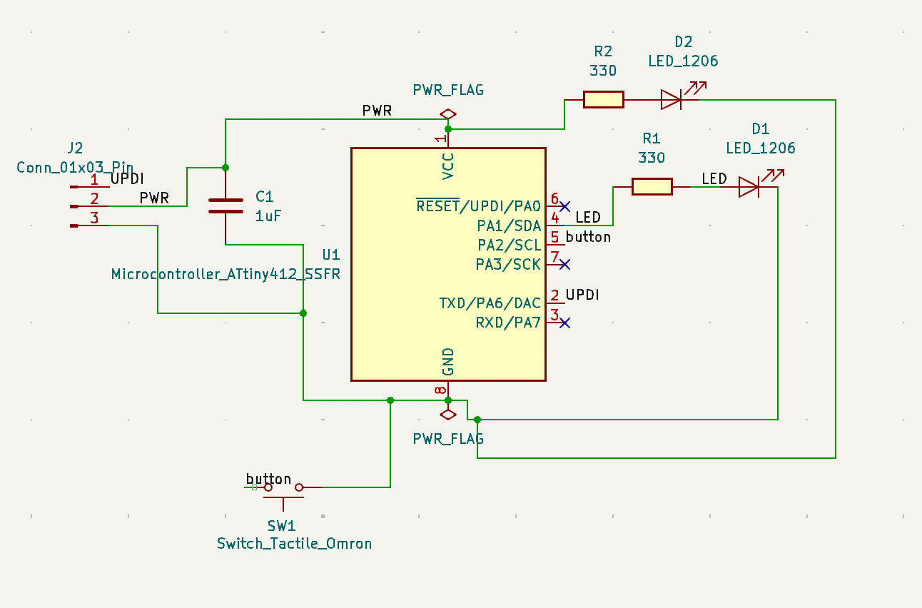
I ended up including two LEDs, one that is directly connected to VCC and GND, and another that is connected to a pin and GND. This allows me to see whether there a current supplied to the LEDs when I produce the board.
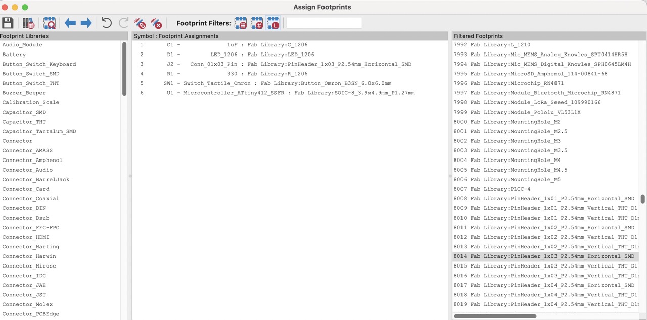
This circuit was a good transition into the charlieplexing PCB I would later design, as there were existing models in previous year’s documentation. After going through the ERC and getting rid of all the errors, I began assigning footprints to each symbol. All of the smd components could easily be found in the Fab library (phew!).
Opening up the PCB layout editor, I set up the constraints/stackup the exact same way as I did before.
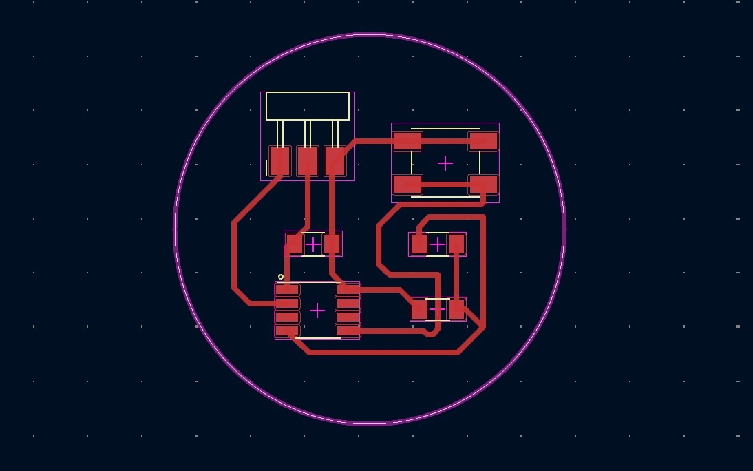
I then created an 18mm diameter circle on the edge cuts layer. I began arranging my components and seeing how they were going to be routed. This was definitely the most tedious part, as Neil mentioned that poor placement can make routing quite difficult. In term of the trace thickness, I talked to Fab Graduate Pari Hathiram, and she suggested .5 mm.
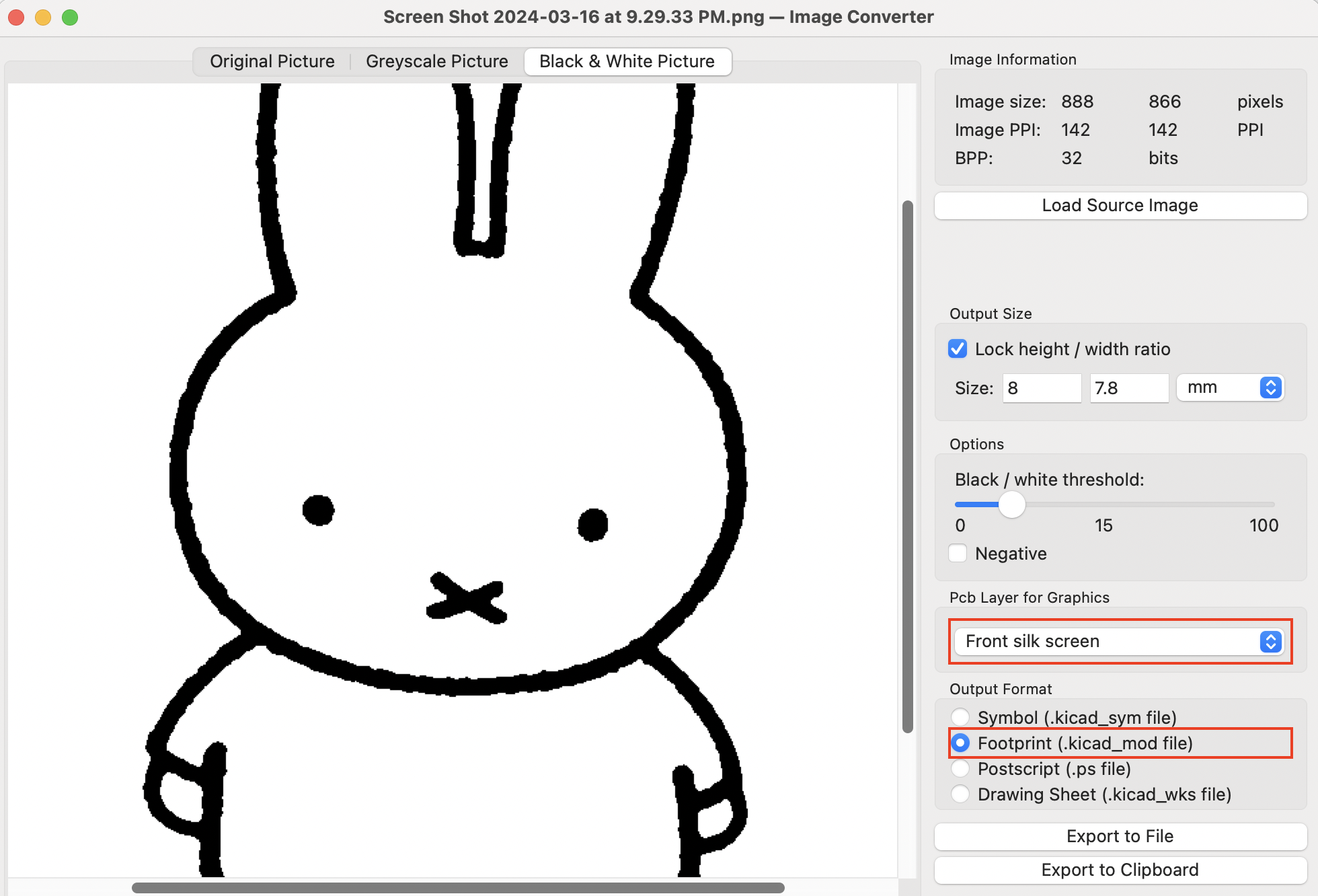
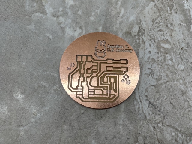
As a more decorative aspect of this design, I also chose to add text and graphics. I opened up the image converter workspace of kicad and imported an image of miffy. Scaling it down, I selected front silk screen as the layer and footprint for the output format.
Yay! The board is miffy themed now!!


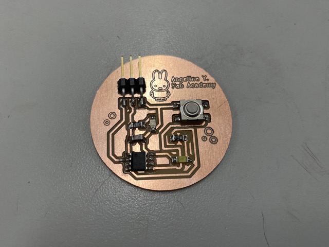
Finished board and 3D model with the additional LED added in
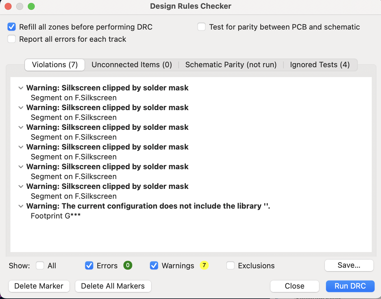
For the most part, there weren’t any errors with my board when I ran the DRC. However, there were a couple of errors about the silkscreen being clipped by the solder mask. I ultimately ignored these as they didn’t impact the actual board.
Producing the Blink Board
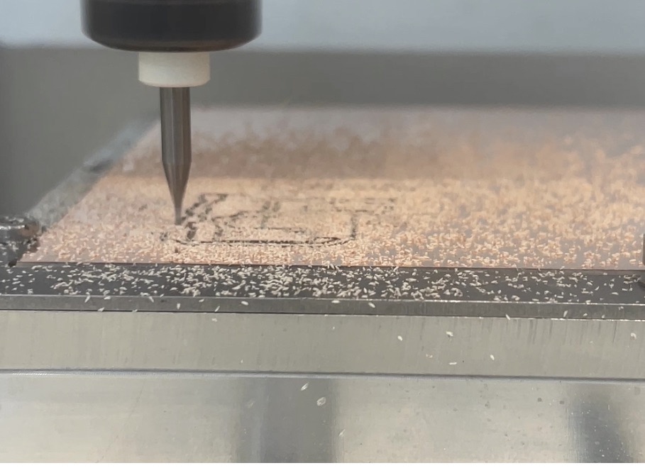
Because this board had a particularly detailed engraving, I needed to use the 1/100” bit (fingers crossed that I didn’t break it). I first used the plot command and created a new folder for these Gerber files. Importing the F.Cu, F. Silkscreen, and Edge cuts layer into the Bantam software, I selected the appropriate tools (1/100” for engraving, 1/64” for traces, 1/32” for traces and outline), performed the automatic z-probe, and milled the file(s). There were no major issues during this process, except during the tool installation process, in which the milling machine failed to detect the bed and kept descending. This was easily solved by restarting the software and cleaning off the bit/bed.
No video this time because my phone ran out of storage :(
Components for the Miffy Blink Board
| Component | Quantity |
|---|---|
| ATtiny412 | 1 |
| Blue LED | 1 |
| White LED | 1 |
| 3-pin SMT male header (FTDI) | 1 |
| 499 1206 SMD resistor | 2 |
| 970 nF capacitor (~1uF) | 1 |
| Milled PCB | 1 |
| Tactile switch | 1 |
Before soldering, I was worried that the 1/64” bit didn’t fully cut through the traces, so I went back in with a razor blade and ensured that the connections were distinct.
I followed the references on my schematic and PCB layout to make sure that my components with polarity were oriented correctly. The F. Fab layer was particularly helpful during this step!
Ready for testing!!
When I was ready for testing this board, I decided to use the Arduino again with the attiny blink board acting as a programmer. I uploaded the jtag2updi sketch again to Arduino Uno, wrote up a simple blink code (selecting ATtiny412 as the board now), and uploaded it. Unfortunately, the console indicated the exact same UPDI initialization issue I ran into a couple of weeks ago.
pymcuprog.pymcuprog_errors.PymcuprogError: UPDI initialisation failed
I immediately looked towards the connections on my board and noticed that I had mixed up PA6 and the physical pin 6 for the UPDI. As a temporary fix, I used jumper wires to directly connect the Arduino to pin 6 and uploaded my code.
Blue and white to fit the miffy theme :>
Although this board was faulty, it was a good introduction to electronics design, and it served as a solid reference for my future boards!
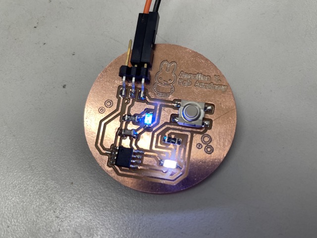
Designing a Charlieplexing board
In an effort to expand my horizons and challenge myself, I wanted to make a more expressive and multi-functional board, encompassing more LEDs, connector pins, etc. So begins the journey…
Resources
I wanted to use the ATtiny412 again with my new design considerations, but I wasn’t sure how to control a lot of LEDs with a limited number of pins (or if I even could). Curious, I looked around for some inspiration:
Charlieplexing is used to drive several LEDs into a fewer amount of pins on a microcontroller, specifically n*(n-1) LEDs where n = number of pins. Its an easy way to incorporate a lot of outputs without taking up too many pins on your microcontroller–the perfect approach for my design with the ATtiny412!
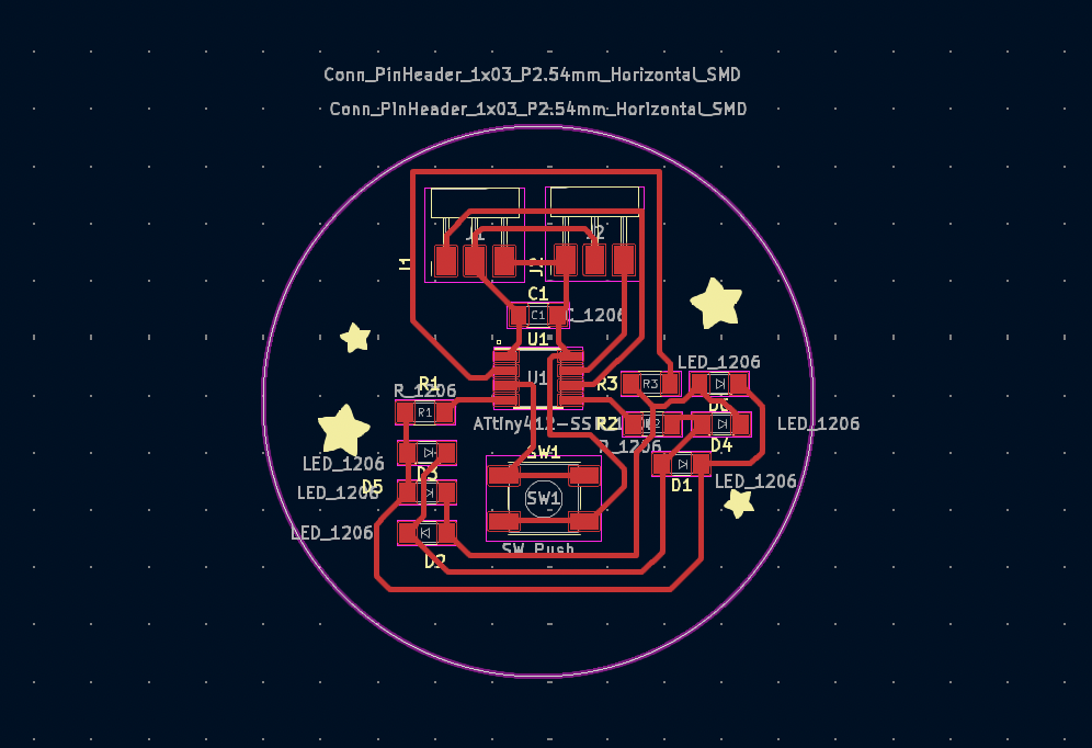
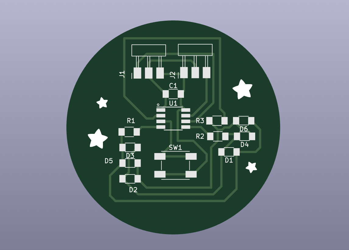
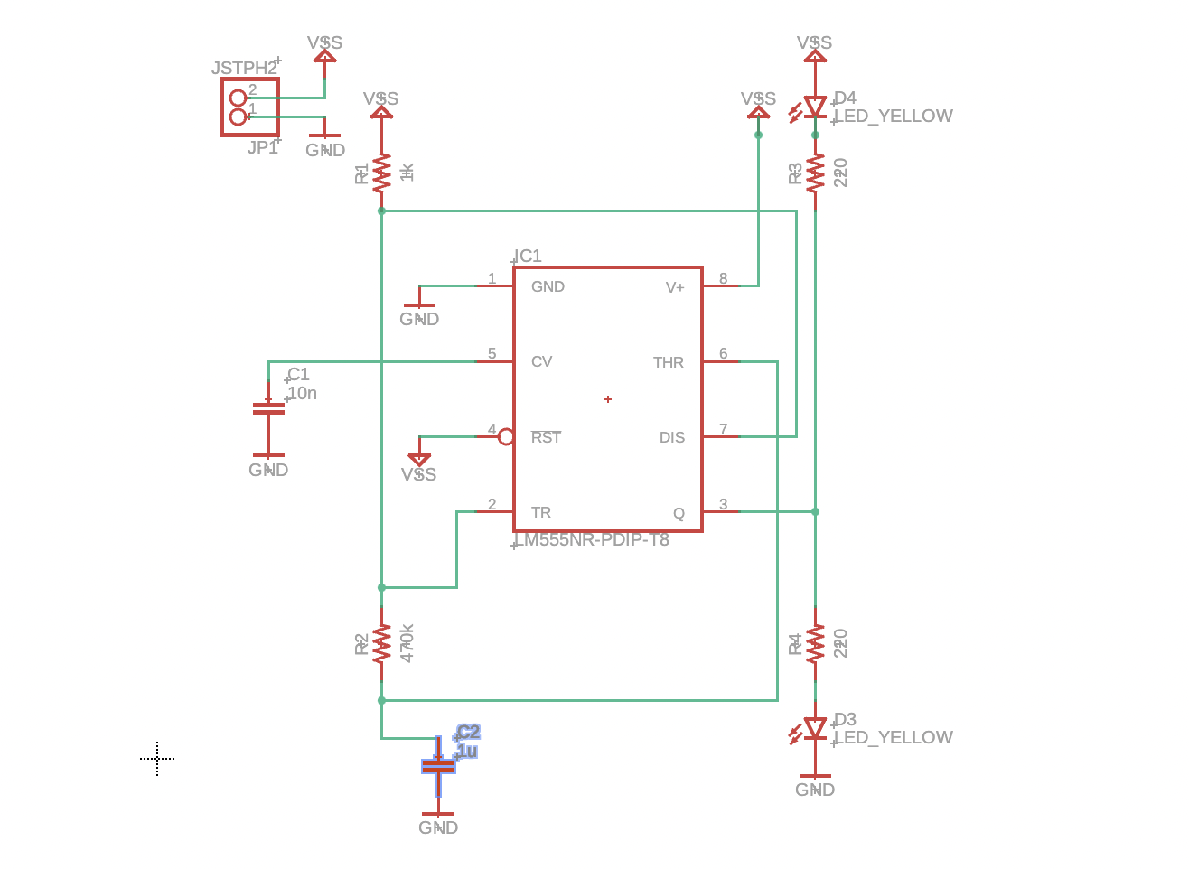
To begin, I opened up another schematic and began replicating a simple charlieplexing circuit with three signal pins (one HIGH, one LOW, and one input). For this PCB, I also wanted to practice some more of the organization techniques that the tutorials suggested. This included using net labels and boxes to split the schematic into specific units.
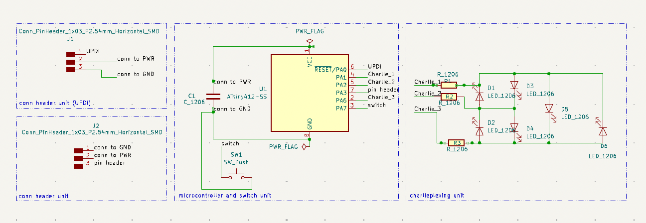
This circuit has two sets of pin headers for the UPDI and a separate sensor/component/etc.
Because this circuit was relatively similar in nature to the blink board, finding the footprints was fairly easy. I ensured that the Fab libraries were installed, and I selected the same components.
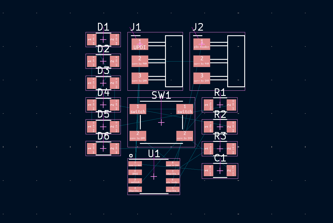
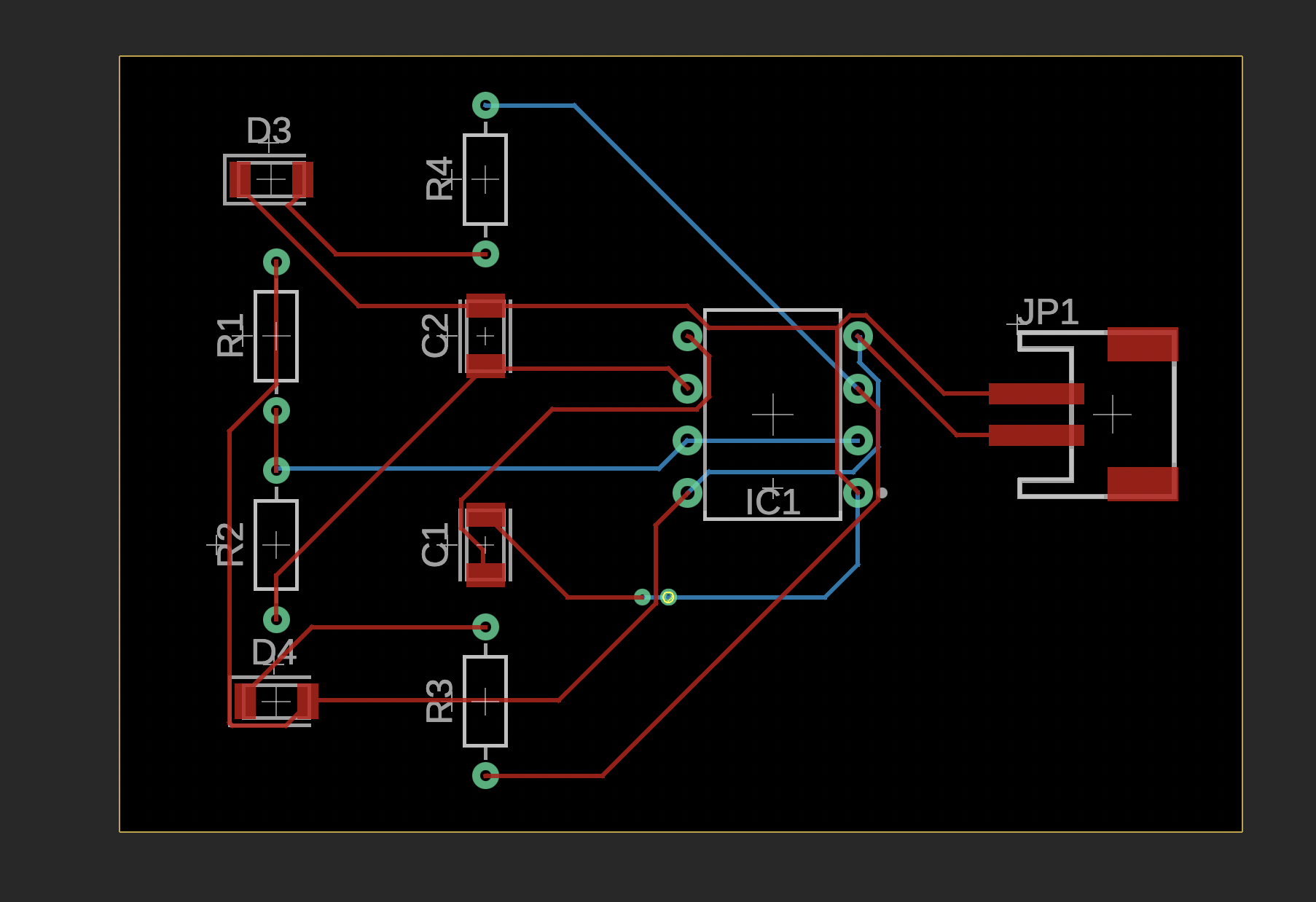
In contrast, routing the traces for this circuit was a nightmare. I wanted to avoid using vias or the bottom layer, which made routing around the pin headers and the button particularly difficult. After a couple of tries (and a lot of frustration), I came up with these traces.
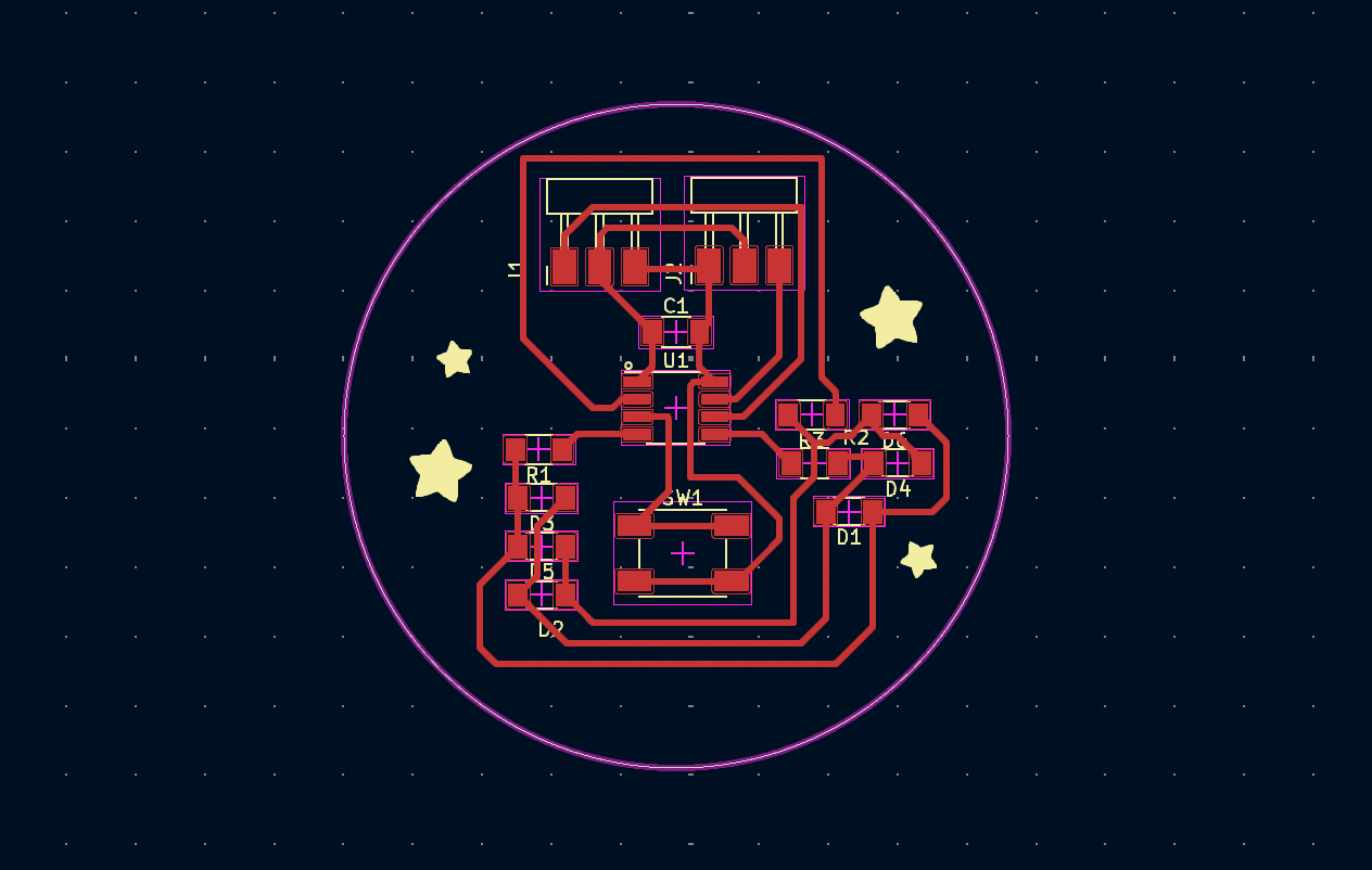
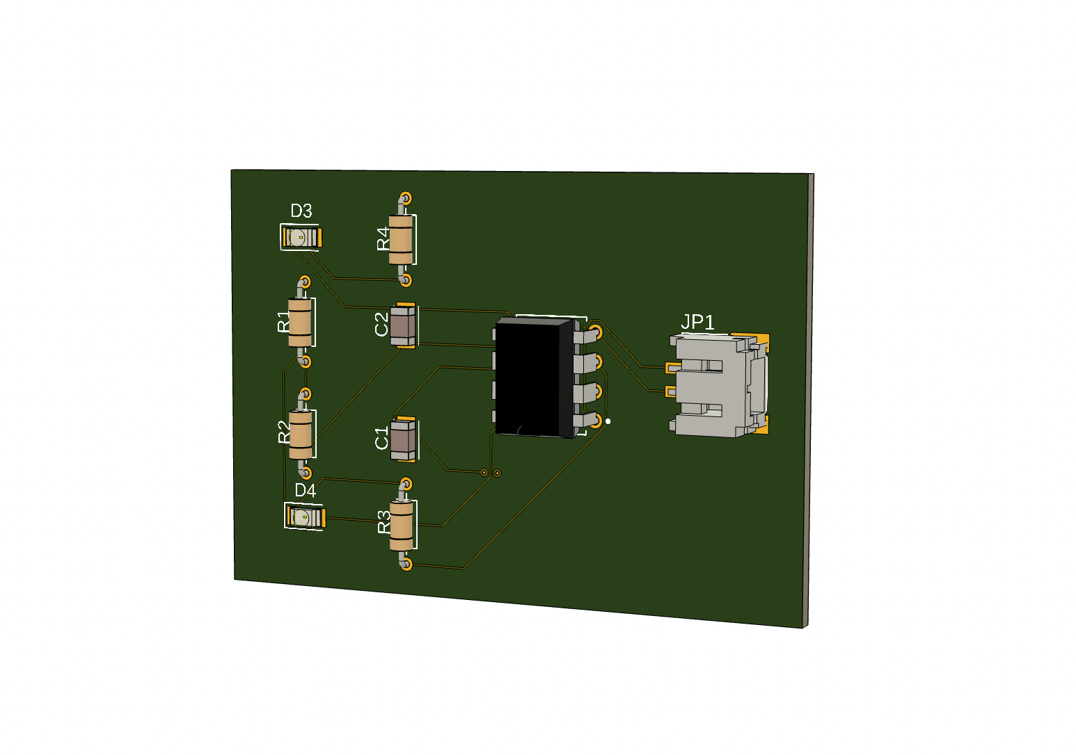
I wanted to make this board customized, just like the previous blink board. Though I ended up not adding a kirby graphic, I still included stars :)
Here is the board with the component labels (F. Fab) and the 3D model:
Producing the Charlieplexing Board
I milled this board with the same settings (more documentation found on Electronics Production), and there were no issues. The only difference between this board’s graphics and the miffy blink board was that the stars didn’t require an extremely thin bit (1/64” worked fine).
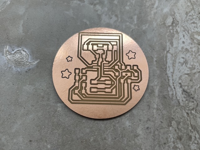
The traces were a lot cleaner this time!
I then soldered the following components on their respective pads, referencing the PCB layout again.
Components for the Charlieplexing Board
| Component | Quantity |
|---|---|
| ATtiny412 | 1 |
| Orange LED | 2 |
| White LED | 2 |
| Red LED | 2 |
| 3-pin SMT male header (FTDI) | 2 |
| 499 1206 SMD resistor | 3 |
| 970 nF capacitor (~1uF) | 1 |
| Milled PCB | 1 |
| Tactile switch | 1 |
Now, onto testing!! While learning about Charlieplexing initially, I remembered that two pins represent OUTPUTs and the third represents an INPUT. By creating different combinations (and setting different charlieplexing pins to INPUT), I could create six different scenarios, one for each of the LEDs. My C++ knowledge is still quite limited, so I ended up taking the long way of programming this board, by writing out all of the combinations.
#define CHARLIE_A 0 // defines pins for the charlieplexing pins
#define CHARLIE_B 3
#define CHARLIE_C 2

void setup() {
  // put your setup code here, to run once:
  pinMode(CHARLIE_A, OUTPUT);
  pinMode(CHARLIE_B, OUTPUT);
  pinMode(CHARLIE_C, OUTPUT);

}

void loop() {
  // put your main code here, to run repeatedly:

  // first LED
  pinMode(CHARLIE_A, OUTPUT);
  pinMode(CHARLIE_B, OUTPUT);
  pinMode(CHARLIE_C, INPUT);

  digitalWrite(CHARLIE_A, HIGH);
  digitalWrite(CHARLIE_B, LOW);
  delay(1000);

  // second LED

  pinMode(CHARLIE_A, OUTPUT);
  pinMode(CHARLIE_B, OUTPUT);
  pinMode(CHARLIE_C, INPUT);

  digitalWrite(CHARLIE_A, LOW);
  digitalWrite(CHARLIE_B, HIGH);
  delay(1000);

  // third LED

  pinMode(CHARLIE_A, INPUT);
  pinMode(CHARLIE_B, OUTPUT);
  pinMode(CHARLIE_C, OUTPUT);

  digitalWrite(CHARLIE_B, HIGH);
  digitalWrite(CHARLIE_C, LOW);
  delay(1000);

  // fourth LED

   pinMode(CHARLIE_A, INPUT);
  pinMode(CHARLIE_B, OUTPUT);
  pinMode(CHARLIE_C, OUTPUT);

  digitalWrite(CHARLIE_B, LOW);
  digitalWrite(CHARLIE_C, HIGH);
  delay(1000);

  // fifth LED

  pinMode(CHARLIE_A, OUTPUT);
  pinMode(CHARLIE_B, INPUT);
  pinMode(CHARLIE_C, OUTPUT);

  digitalWrite(CHARLIE_A, HIGH);
  digitalWrite(CHARLIE_C, LOW);
  delay(1000);

  // sixth LED

   pinMode(CHARLIE_A, OUTPUT);
  pinMode(CHARLIE_B, INPUT);
  pinMode(CHARLIE_C, OUTPUT);

  digitalWrite(CHARLIE_A, LOW);
  digitalWrite(CHARLIE_C, HIGH);
  delay(1000);
}
Sorry for the shaky video :,)
Though it’s technically impossible to light all LEDs at once, you can create the perception by eliminating all of the delay functions. This is exemplified with my board, which is connected to the QuenTorres.
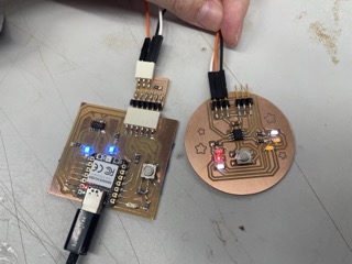
Hero shot of board
Overall, this board is quite versatile in that it can be controlled in several manners (button or through code directly), it contains several LEDs in a limited number of pins, and it can still be used for other outputs, such as neopixels. I hope to potentially use this during outputs week!!
EagleCAD
EagleCAD Tutorial
As a short introduction to EagleCAD, a sub-workspace of Fusion360, I followed this tutorial. It essentially followed the same process as kicad, with the addition of the automatic routing feature (super helpful!!)
Here is a schematic that I made in Eagle!
And here is one of the automated routes that Eagle created, including traces on both the front layer and back layer.
To create a 3D model with the schematic, I hit the Push to 3D PCB option in the toolbar and clicked push.
Overall, I thought that Eagle was a bit more user-friendly in terms of its interface and capabilities. Not only does the toolbar directly reflect Fusion360’s interface, but features such as the automatic routing can be really helpful!
Group Assignment
For this week’s group assignment, I worked with Connor Cruz and Kabir Nawaz. Our task was to explore different settings on the multimeter/oscilloscope to observe a microcontroller’s performance with voltage, current, etc. Additionally, we saw how PWM signals changed with a dynamic LED. You can find our full documentation here
Individual Contribution
My individual contributions consisted of recording and interpreting what the multimeter’s values meant, including the constant voltage from PWR directly to GND, PWM pin (dynamic). Additionally, I wrote up what those values looked like on the oscilloscope.
Reflection
Firstly, thank you to Pari Hathiram and Mr. Dubick for advice on routing and getting started with schematic building!
This week was one of the most challenging for me, mainly because I lacked previous experience with schematic building and softwares like KiCad. Fortunately, with the help of tutorials, peers, and teachers alike, I was able to better grasp how to think about what was necessary to build a circuit, how to construct a schematic, and how to convert it to a physical PCB with footprints. I think I struggled a lot, and at times, I was confident I was going to fail. Without being in the lab especially due to spring break, I was most worried that I would fall behind. However, with patience, time, and a lot of mistakes, I was able to learn a lot more and get a little closer to materializing my final project.